Technology (IJRASET)
Comparison of Power and Delay in Different
Types of Full Adder Circuit
N. Sabari Manoj1, K. Suriya2
1
M.E VLSI DESIGN, Easwari Engineering College, Chennai
2
M. E. Assistant Professor, Easwari Engineering College, Chennai
Abstract— In this review paper 1-bit CMOS full adder cells are studied using standard static CMOS logic style. The comparison is carried out using several parameters like number of transistors, delay, power consumption and power delay product (PDP).The circuits are designed at transistor level using 32nm CMOS technology. Different full adders are studied in this paper like Transmission gate (TGA) ,Static energy recovery factor (SERF),Gate Diffusion Input full adder (GDI), 14 T full adder using XNOR/XOR cell, 8 T full adder using 3 T XNOR gate.
Keywords— PDP, CMOS full adder, power dissipation, low power, logic style, SERF, GDI.
I. INTRODUCTION
The extensive development in the field of portable systems and cellular networks has intensified the research efforts in low power microelectronics. The low-power design has become a major design consideration. The design criterion of a full adder cell is usually multi-fold. Transistor count is, of course, a primary concern which largely affects the design complexity of many function units such as multiplier and algorithmic logic unit (ALU). The limited power supply capability of present battery technology has made power consumption an important figure in portable devices follow. The speed of the design is limited by size of the transistors, parasitic capacitance and delay in the critical path. The driving capability of a full adder is very important because full adders are mostly used in cascade configuration where the output of one provides the input for other. If the full adders lack driving capability then it requires additional buffer which consequently increases the power dissipation. The energy consumed by gate per switching element is known as PDP. The power delay product is a measure of efficiency in an adder circuit. There is a tradeoff between power dissipation and speed and is very important when low power operations are needed [3]. It is given by
PDP =Power * DELAY
Reducing the number of transistors may lead to reduced power but sometime does not improve. All these characteristics of full adder vary from one logic to another logic [4].
II. POWERANDDELAYCOMPARTIVEANALYSISOFFULLADDERCIRCUIT
A. 10 T static energy Recovery full adder
The cell uses only 10 transistors and it does not need inverted inputs. The design was inspired by the XNOR gate full adder
design. In non-energy recovery design the charge applied to the load capacitance during logic level high is drained to ground during the logic level low. It should be noted that the new SERF adder has no direct path to the ground. The elimination of a path to the ground reduces power consumption. The charge stored at the load capacitance is reapplied to the control gates. The combination of not having a direct path to ground and the re-application of the load charge to the control gate makes the energy recovering full adder an energy efficient design. To the best of our knowledge this new design has the lowest transistor count for the complete realization of a full adder.
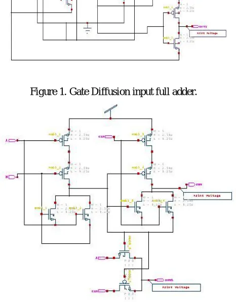
B. Gate diffusion input full adder
C. 8T Full adder using 3T XNOR gate
For 8 T full adder sum is generated by two XNOR gates and Cout is generated by two transistors multiplexer block. The output of the first stage is used as a selector circuit for the carry output. When the output of the first stage a XNOR b is “0”, the carry output is equal to the carry in i.e. ‘Cin’. When the output of the first stage a XNOR b is “1”, the carry output is equal to the input ‘a’.
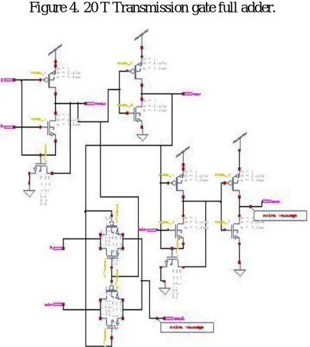
D. 20 T Transmission gate full adder
A CMOS transmission gate is constructed by parallel combination of nMOS and pMOS transistors with complementary gate signals. It gives full swing output so its use give better speed in CMOS circuit but there is no isolation between input and output.
E. 14 T full adder circuit using XNOR/XOR cell
For transmission gate multiplexer complementary gate control signals are required and in 14 transistor full Adder both XOR and XNOR signals are generated.
III. DIFFERENTADDERCIRCUITANDTHEIRCOMPARISON
[image:3.612.185.420.327.483.2]Different full adder circuits are given here and simulated using Tanner EDA tool. The simulation is carried out in 32 nm CMOS process technology at 3.3 Vdd. The comparison of various full adders is done using different parameters like power consumption, delay, PDP and number of transistors used and simulation results of adders discussed above are given in the Table 1.
Figure 1. Gate Diffusion input full adder.
[image:3.612.194.427.409.707.2]Technology (IJRASET)
[image:4.612.197.419.446.695.2]Figure 3. 8 T full adder using 3 T XNOR gate.
Figure 4. 20 T Transmission gate full adder.
Cell name Power consumpti on(Watts)
Delay PDP(FJ) No of transistors
Transmiss ion gate adder
8.43E-02 1.00E-09 8.43E-11 20
14 T full
adder 2.93E-02 7.47E-10 3.17E-16 14
GDI full
adder 4.24E-07
2.69E-07
7.87E-09 10
SERF full
adder 1.50E-10
8.73E-09
1.31E-18 10
8 T full
adder 7.35E-11
6.37E-07
4.68E-17 8
IV.CONCLUSION
The performance of various full adders given in Table-1 shows that different adders have different parameter values no single adder have less delay, power and PDP. So there is a tradeoff between these parameters. The results help us to choose an adder which can give us desired result according to a specific application.
REFERENCES [1] N. Weste, K. Eshragian, Principles of CMOS VLSI Design: A Systems
[2] Perspective, Addison-Wesley, 1993.
[3] A. Chandrakasan, S. Sheng and R.Brodersen, “Low-power CMOS digitaldesign,” IEEE Journal of Solid StateCircuits.” IEEE Journal of Solid StateCircuits, Vol. 27, No 4, pp. 473-484,April1992.Clarendon, 1892, pp.68-73.
[4] J. Wang, S. Fang, and W. Feng, “New efficient designs for XOR and XNOR functions on the transistor level”, IEEE J. Solid-State Circuits, vol. 29, no. 7, Jul. 1994, pp. 780–786.
[5] S. Goel, A. Kumar, M. A. Bayoumi, “Design of Robust, Energy-Efficient Full Adders for Deep-Submicrometer Design Using Hybrid-CMOS Logic”, IEEE Transactions on VLSI 2006.
[6] Amir Ali Khatibzadeh, Kaamran Raahemifar, “A study and comparision of full adder cells based on the standard CMOS logic,” IEEE Trans.CCECE, Niagara Falls, May 2004 0-7803-8253, pp. 2139-2142.
[7] Ming-Bo Lin, “Introduction to VLSI systems A logic, circuit and system perspective,” Taylor & Fransis group, ch. 7 .