HP 150 Personal Computers
HP 150
TECHNICAL
Reference Manual
Product No. 45625A
FliP'W
HEWLETTa:e..
PACKARDPersonal Office Computer Division
Purpose: This manual provides detailed technical int'ormation on the internals of the HP 150 hardware, firmware, and software. It is designed to aid in the development of hardware and software products which will become part ot', or work
in conjunction with, the HP 150.
User Level: Use of this information assumes a background in digital logic and assembly-language programming.
Related Products: The HP 150 Progr-wuller's Tool Kit (Product 45435A) contains the Assembler, Linker, and appropriate documentation. The HP 150 ~-DOS User's Guide (Product 45624A) provides details on KS-DOS.
COmpatibility: A hardware/software product designed to be dependent on one specific vers ion of the HP 150 hardware, firmware, or software may be
incompatible with other versions of the HP 150 -- or such a product may be incompatible with future personal computer products from Hewlett-Packard, including models based on the HP 150 itself.
Support: Because of the specialized nature of this information, the many capabilities of the HP 150 when used at this level, and the importance of design strategy for successful implementation of hardware/firmware-based products, assistance in the use of this manual is provided through local consulting --available ~ the hour (Product 45686A) or ~ the day (Product 45687A). Contact your local HP Sales and Service Office - - ask for Personal Computer Systems Engineering.
NOTICE
The information contained in this document is subject to change without notice.
HEWLETT-PACKARD MAKES NO WARRANTY OF AlfY KIND WITH REGARD TO THIS MATERIAL, INCLUDING, BUT NOT LIMITED TO, THE IMPLIED WARRAHTIES OF MERCHANTABILITY AND FITNESS FOR A PARTICULAR PURPOSE. Hewlett-Packard shall not be liable for errors contained herein or for incidental or consequential damages in connection with the furnishing, performance or use of this material.
Hewlett-Packard assumes no responsibility for the use or reliability of its software on equipment that is not furnished by Hewlett-Packard.
This document contains proprietary information which is protected by
copyright. All rights are reserved. No part of this document may be photocopied, reproduced or translated to another program language without the prior written consent of Hewlett-Packard Company.
LIST OF EFFECTIVE PAGES
The List of Effective Pages gives the date of the current edition, and lists the dates of all pages of that edition and all updates. Within the manual, any page changed since the last edition is indicated by printing the date the changes were made on the bottom of the page. Changes are marked with a vertical bar in the margin. If an update is incorporated when an edition is reprinted, these bars and dates remain. No information
is incorporated into a reprinting unless it appears as a prior update.
First Edition •.•.•••.••.••. May
1984
Effective Pages Date
New editions are complete revisions of the manual. Update packages, which are issued between editions, contain additional and replacement pages to
be merged into the manual by the customer. The date on the title page and back cover of the manual changes only when a new edition is published. When an edition is reprinted, all the prior updates to the edition are incorporated. No information is incorporated into a reprinting unless it appears as a prior update. The edition does not change.
PREFACE
I
CAUTIONI
This document provides detailed technical information revealing internal details of the UP 150 hardware, firmware, and software.
The information presented allows development of hardware and software products for the UP 150 which may be incompatible with future personal computer products from Hewlett-Packard, including models based upon the UP 150
itself.
This manual presents technical information concerning the UP 150 Personal Computer and covers its hardware, firmware, and software subsystems.
This manual consists of the following sections and appendices:
Section 1 - Introduction provides an overview of the UP 150.
Section 2 - Hardware Overview provides product specifications information and briefly describes each subsystem of the BP 150.
Section 3 - Hardware Subsystems contain detailed information on the UP 150's hardware subsystems and helpful des ign hints.
Section 4 - Memory and I/O Mapping provides information on the memory and input/output bit mappings of the system's processor.
Section 5 - System Software provides information on the
operating systems, device drivers, MS-DOS calls,
AGI_OS, BIOS, configuration, and disc format structure.
Section 6 - System Firmware provides mapping informai ton on system RAM memory.
Section 7 - Programming the HP 150 contains programming information on escape sequences, MS-DOS, AGIOS,
alphanumeric and graphics displays, datacomm, keyboard, HPIB, and accessory card interfacing.
Section 8 - AGIOS Function Call Reference provides a reference list of AGIOS function calls.
Appendix A - Logic Diagrams contain schematic diagrams of the UP 150.
T
ABLE
OF CONTENTS
I
Section 1 - INTRODUCTION
HP 150 System Overview . . . • . . . • . . . • • . . . 1-1 System ~chi tecture . . . 1-1
Display. . . . . .. . . . 1-2
Keyboard . . . • . . . • . . . • . . . • . . . 1-3 CommWlications . . . 1-3 Section 2 - HARDWARE OVERVIEW
In troduct ion . . . 2-1 Product Specifications . . . • . . . • . . . 2-1 General Description .. > • • • • • • • • • • • • • • • • • • • • • • • • • • • • • • • • • • • • • • • • • • • • • • • • • • • • 2-1
Physical Specifications . . . • • . . . • • • . . . • . . • . . . • . . . 2-2 Environmental Specifications . . . • . . . • . . . • . . . 2-2 Product Regulations . . . • . . . . • . . . . • . . . • . . • . . . • . . . • • . . . 2-3 Power Requirements . • . . . • . . . • . . • . . . • . . • . • . . . . • . . . • . . . . 2-3 CommWlications . . . • . . . • . . . 2-3 Subsystem Power Requirements ...••....•..•..•...••..•..•.•...••... 2-3 HP 150 Printed Circuit Assemblies . . . • . . . • . • . • • • . . • . . . 2-5 Analog Boards . . . • . . . • • • . • . . . 2-6 Digital Logic Boards . . . • • . . . . • . . . • . . • . . . • . . . 2-6 Section 3 - HARDWARE SUBSYSTEMS
Front Plane .... , . . . 3~1
Keyboard and Touchscreen Subsystem . . . 3-37 Keyboard . . . 3 - 3 7 Touchs creen . . . , . . . • . . . 3 - 38 Specifications . • . . . 3-40 Timing . . . ' . . . 3-40 8041 Keyboard/Touchscreen Scanner . . . 3-44 Da tacomm Subsystem . . . • . . . 3 - 50 General Description . . . 3-50 RS232C/422 Datacomm Module Connector . . . 3- 50 Baud Rate Genera tor . . . 3 - 51 Multi-Protocol Controller . . . 3-52 Communicatons Interface Circuitry . . . • . . . 3-53 Mezzanine Memory Subsystem . . . 3-55 Mezzanine Memory PCA . . . 3-55 PCA Overview . . . 3-55 Conne ctor Signals . . . • . . . 3 - 57 ROM . . . 3-59 Slot Selection Generation . . . 3-60 CMOS RAM . . . • . . . 3-61 LEDs . . . 3-62 Dynamic RAM •••••••••••••••••••••••••••••••••••••••••••••••••••••••••••••• 3-62 Accessories Subsystem . . . 3-64 Accessory Hardware Des ign Guidelines . . . • . . . 3-64 Mechanical Specifications . . . 3-64 Power Requirements . . . 3-64 Thermal Limits . . . 3-65 Accessory Signal Loading Restrictions . . . 3-65 Signal Timing Diagrams . . . 3-67 Accessory Front Plane Connector . . . 3-'(0 Accessory Connector Signal Descriptions . . . 3-71 Accessory Card Hardware and Electrical. . . 3-73 Electrical Des ign . . . 3-73 Mechanical Design . . . " . . . 3-76 Drawings . . . 3-80
Section 4 - MEMORY AND I/O MAPPING
Memory Mapped Devices . . . , ... 4-1
T ABLE OF CONTENTS (Continued>1
Data Row Register (R1) . . . • . . . 4-6 Data Row End Register (R12) . . . 4-6 Auxiliary Address Register 2 (R13 and R14) . . . • . . 4-7 Start Command (R15) . . . 4-7 Reset Command (R16) . . . • . . . 4-7 Smooth Scroll Offset Register (R17) . . . • . . . • . . . 4-7 Vertical Cursor Control Register (R18) . . . • . . . • . . . 4-7 Horizontal Cursor Register (R19) . . . 4-7 Cursor Registers R38 and R39 (READ) . . . • . . . 4-7 Interrupt Enable Register (R1A) . . . 4-7 Status Register (R3A) . . . 4-8 Vertical Light Pen Register (R3B) . . . 4-8 Horizontal Light Pen Register (R3C) . . . • 4-8 Video Attribute Latch . . . • . . . 4-8 I/O Mapped Devices . . . • . . . . 4-9 HP 150 Input/Output Map . . . • . . . 4-9 Real Time Clock (MM58167A) . . . • . . . 4-10 Integral Printer Interface . . . • . . . 4-11 Keyboard/Touchscreen Controller (8041A) . . . • . . . 4-11 Datacomm Port 1 Control Lines/Manuf Test nepeat . . . • . . . 4-12 Datacomm Port 2 Control Lines/Clock Source Select . . . • . . . • . . . 4-12 Interrupt Controller (8259) . . . • . 4-13 Baud Rate Genera tor (8116T) . . . • . . . • . . . 4-13 HPIB Controller (9914) . . . 4-11.4 MPSC - Dat~cQmm Controller (7201/8274) . . . 4-14 Section 5 - SYSTEM SOFTWARE
I
TABLE OF CONTENTS (Continued)
How a Program Terminates . . . 5-13 Conditions in Effect When a Program Receives Control . . . 5-13 Transient Portion of COMMAND. COM . . . 5-15 HP 150 Devices . . . 5-16 Logical (Mappable) Devices . . . • . . . 5-16 Phys ical Devices . . . 5-16 Mapping Logical to Physical Devices . . . 5-16 The Device Configuration Utility . . . 5-17 Installable Devices . . . • . . . 5-18 Character Devices and Block Devices . . . 5-20 How Application Programs Can Get to Devices . . . 5-20 Device Driver Structure . . . 5-21 Pointer to Next Device Field . . . 5-22 Attribute Field . . . 5-22 Strategy and Interrupt Routines . . . 5-23 Name Field . . . 5-23 Device List . . . 5-24 How to Create a Device Driver . . . • . . . • . . . 5-26 How MS-DOS Calls a Device Driver . . . • . 5-27 Request Header . . . 5-27 Unit Code . . . 5-27 Command Code Field . . . • . . • . . . . • . . . 5 -28 Status Word . . . . • . . . • . . . • . . . 5 -28 Device Driver Functions and Parameters . . . 5-31 Ini t . . . 5-31 Media Check . . . • . . . • . . . 5-32 Build BPB (BIOS Parameter Block) . . . • . . . 5-33 Read or Write . . . • . . . 5-35
Non-Destructive Read No Wait . . . " . . . 5-36 Status . . . • . . . 5-37
Flush . . . • . . . 5 -38 HP 150 Installable Device Driver Example . . . 5-39
AGIOS: I/O Control of the Con Device . . . 5-49
The Alpha/Graphic Input/Output System (AGIOS) . . . 5-49 Accessing the AGIOS . . . 5-49
BIOS and Its Devices . . . 5-51
Introduct ion . . . 5 -51 The CONFIG. SYS File . . . 5-55
Disc Format and Directory Structure . . . • . . . 5-57
Phys ical Disc Format... . . . 5-57
Disc Media Storage Capacity . . . 5-57
Disc Sector Allocation . . . 5-58
Header Record. . . . . . . . . . . . . . . . . . . . . . . . . . .. . . . 5-59
T ABLE OF CONTENTS (Continued>1
Section 6 - SYSTEM FIRMWARE
Firmware Memory Map ...•...•...•...•..•.••...••.... 6-1
RAM ••••••••••••••••••••••••••••••••••••••••••••••• •••••••••••••••••••••••• 6-1
Firmware Entry Point Jump Vectors .•...•...••...•... 6-1
Section 7 - PROGRAMMING THE HP 150
Generating Es cape Sequences ...•...•....•...•..•..••... 7-1 Performing MS-DOS System Function Calls •...•...•...••...•.•. 7-2 Making AGIOS Function Calls ...•...•...•...•...•••.••...••..•...••. 7-5 Alphanumeric Display Interfacing ....•...•...••...•. 7-8 Alphanumeric Video RAM Structure .•...•...••...•.•.•.. 7-8 Alpha Video Buffer Format ...•...•.•..••...•...•..•. 7-8 Video Row Pointer Table Format ...•..•...•.•..••...•. 7-9 Row Pointer Formulation . . . • . . . . • • . . . • • . 7-9 Line Buffer Format . . . • . . . • . . . • . . . • • . . . • . . 7-10 Enhancement/Character Set Byte Structure . . . • . . . 7-10 Character Code Structure ...•...••....•.•....•...•... 7 -10 Finding Row Pointer Table Origin ...•.•.••...•..••••...•...•. 7-11 Fetching Row Pointers from the Table ...•.•.•..•..••..•....•...•... 7-12 Placing a Character in Alpha Memory ...•...•...•..•..•••.•••..••...• 7-13 Writing to Lines 25, 26, and 27 ...•..••...•••....•••.•••...•..•.•.•• 7-15 Graphics Display Interfacing ...•...•...•..•..••••...••.••.•••..• 7 -18 Keyboard Interfacing ...•...•••••••...••.•...•...•.. 7 -~2
Keycode Mo~e . . . 7-~2
Console RAW/COOKED Mode .•..•••...•...••••...•....•...•.•....•... 7- 3
I
TABLE OF CONTENTS
(Continued)
HPIB Control Calls ..••.•••..• MS-DOS IOCTRL Function Call. Control Block Format ....• Control Template Format. Sample Identify Templates •.
Sample Read/Write Buffer Templates.
HPIB Interface Example (9111A Graphics Tablet). Accessory Card Interfacing ••...••..•••.
Memory (Slot) Address Identification ••
Section 8 - AGIOS FUNCTION CALL REFERENCE Syntax Used in the AGIOS Function Calls. Batch Function Call ..
Video Intrinsics. Define Area .•• Write Area. Clear Area. Enhance Area •• Read Area .• Shift Area. Write Line.
Application Softkeys. Update Softkey Label .• Read Softkey Label .... Display Softkey Labels ... Control Functions ...•...
Execute Two Character Sequence Position Cursor (ESC
&
a) ... Define Enhancements (ESC&
d). Cursor Sense Absolute (ESC a) •. Cursor Sense Relative (ESC ') .. Set Cursor Type ••••••••Read Cursor Type ... .
Read Terminal Configuration. Touchscreen Functions.
Field Operations ... Row Column Operations.
Define Touch Field (ESC - z g).
(ESC Char} ••.
Define Delete
z s).
Softkey Field (ESCTouch Field (ESC - z d). Touchscreen Reset (ESC z j) ..
Set Touch Reporting Mode (ESC - z n). Keyboard Intercept ... .
Define Key Characteristics. Get Key Characteristics. Put Key ... .
Keycode On/Off. Keycode Status ..
. ...
.7-53 .. ... 7-53 · .. 7-53 · .7-54 .7-56 · .7-57 .. 7'"58 · .7-65 · .7-65
• .• 8-1 · .8-2
· .8-4
. ... . 8-5
. ... 8-5 · .8-6 · .8-6 .8-6 · ... 8-7
· .8-8 · .8-9 • ••. 8-9 .8-9 • •• 8-10 .8-11 . .•... 8-11 .... 8-12
. ... . 8-13 · .8-13
· .8-13 · .8-14 .8-14 · .. 8-14
TABLE OF CONTENTS (Continued>1
Read Keypad Status... 8 -23
Display Control ·(ESC • d) . . . 8-24 Clear Graphics Memory (ESC • d a) •••••.•..••..•.••..•...••.••...••.•.••.. 8-24 Set Graphics Memory (ESC • db) ...•..•..•..•...•..•...•.•...•.••.••.. 8-24 Turn On Graphics Display (ESC • d c) ••••••••••••••••••••••••••••••••••••• 8-24
Turn Off Graphics Display (ESC • d d) .•.•••..••..•.•...•.•••.•••....•.••. 8-25 Turn On Alphanumeric Display (ESC • d e) ...•...••.••.•.•..••••••.••..•• 8-25 Turn Off Alphanumeric Display (ESC • d f) ....••..•..•..••..••.•••...•.• 8-25 Turn On Graphics Cursor (ESC • d k) ...•...••••••.•.•.•.•.••.•.••.. 8-25 Turn Ofr Graphics Cursor (ESC • d 1) .••••••.••••••••••••••••••••••.•••••• 8-26 Turn On Rubber Band Line (ESC • d m) ..•••.•....•••....•••.•...•••.•..••.. 8-26 Turn Off Rubber Band Line (ESC • d n) ...•....••.•..••••••.•••..•...••. 8-26 Move Graphics Cursor Absolute (ESC
*
d <x,y>0) ...
8-26Move Graphics Cursor Incremental (ESC • d <x,y> p) .•...••...••.•. 8-27 Turn On Alphanumeric Cursor (ESC • d q) ..•...•.•...••.•.•.••.•••••••••••. 8-27 Turn Off Alphanumeric Cursor (ESC • d r) .•...•..•...••.•••...•.•. 8-27 Turn On Graphics Text Mode (ESC • d s) ••.•..••...•..•...••..••....•.... 8-28 Turn Off Graphics Text Mode (ESC • d t) •.••...••.•••.•.•.•.•.••..•••.. 8-28 Vector Drawing Mode (ESC
*
m) ...•...•••••.••..•.•...•....•..•... 8-29 Select Drawing Mode (ESC*
m <mode> a) ...•...•...••....•..•...•. 8-29 Select Line Type (ESC*
m <type> b) ..••••..•••.•.•.•...•..••...•.•••••. 8-29 Define Line Pattern and Scale (ESC*
m<pattern><scale>c) ...••..•.••.... 8-30 Define Area Fill Pattern (ESC • m <pattern> d) .•...•..••..••...•••..•.... 8-30 Fill Rectangular Area, Absolute (ESC*
m <x1,y1',x2,y2> e) •.•....•.•••.•.. 8-31 Fill Rectap~lar Area, Absolute Relocatable(ESC
*
m <x1,y1,x2,y2> f) ..••...••....•.•....•..•.•.••••••..•••••••••••.. 8-31 Select Polygonal Fill Pattern (ESC*
m <pattern> g) ••.•••••••••••••••••.• 8-31 Select Boundary Pen (ESC*
m <pen> h) ...••...•.••...•..•... 8-32 No Polygon Boundary (ESC*
m h) ...•..•....•.••...••.•...•..•..•. 8-32 Set Relocatable Origin (ESC*
m <x,y> j) . . . 8-33 Set Relocatable Origin to Pen Position (ESC*
m k) .••...•.•. 8-33 Set Relocatable Origin to Cursor Position (ESC· m 1) •.•..•.••••••.•.•.•. 8-33 Graphics Text (ESC .) ...•..•...••..•...•...•..•. 8-34 Set Graphics Text Size Text Size (ESC*
m <size> m) •••••••••••••••••••••• 8-34 Set Graphics Text Orientation «ESC*
m <orientation> n) ...•... 8-34 Turn On Text Slant (ESC*
m 0) •••••••••••••.••••••••••••••••••••••.•••••• 8-35Turn Off Text Slant «ESC
*
m p) ....•...•...•... 8-35 Set Graphics Text Origin (ESC*
m <0-9> q) •..•••••.•..•...•..••..•..•..•. 8~36Vector Draw (ESC
*
p b <x,y» . . . • . . . 8-41 Plot to Cursor Position (ESC*
P c) . . . • . . . 8-42 Point Plot (ESC*
p d) . . . • . . . 8-42 Set Relocatable Origin to Pen Position (ESC*
P e) . . . • . . . 8-42 Start Polygonal Area Fill (ESC*
p s) . . . • . . 8-43 Terminate Polygonal Area Fill (ESC*
P t) . . . 8-43 Polygon Move . . . • . . . . 8-43 Po lygon Draw . . . 8 - 44 Lift Boundary Pen (ESC*
P u) . . . • . . . 8-44 Lower Boundary Pen (ESC*
P v) . . . • . . . • . . . . 8 - 45 Graphics Status (ESC*
s) . . . • • . . . 8-46 Read Device ID (ESC*
s 1) . . . • . . . 8-46 Read Pen Position (ESC*
s 2) . . . • . . . • . . . 8-46 Read Cursor Position (ESC*
s 3) . . . 8-47 Read Cursor Position, Wait for Key (ESC*
s 4) . . . 8-47 Read Display Size (ESC*
s 5) . . . 8-48 Read Graphics Settings (ESC*
s 6) . • . . . • . . . 8-48 Read Graphics Text Status (ESC*
s 7) . . . . • . . • . . . . • . . . • 8-49 Read Zoom Status (ESC*
s 8) . . . • . . . • . . . 8-49 Read Relocatable Origin (ESC*
s 9) . . . 8-50 Read Reset Status (ESC*
s 10) . . . 8-50 Read Area Shad ing (ESC*
s 11) . . . 8 - 51 Read Dynamics (ESC*
s 12) . . . 8-51 Read Extended Screen Dimen'sions . . . • . . . 8-52 Appendix A - LOGIC DIAGRAMS~1_NT_R_O_D_U_CT_I_O_N
____________
~lri!H1'
HP 150 System Overview System Architecture Display
Keyboard
Communications/Peripherals
CONTENTS
1-1 1-1
Introduction
HP 150 SYSTEM OVERVIEW
The HP 150 Personal Office Computer, the third member of the Series 100 family, offers a complete business solution and gives the customer more power and memory space in a small, effic ient package. The entire sytem (display, processor, keyboard, flexible and Winchester disc drives, and integral printer) occupies only 2.1 square feet of space, about the same "footprint" as an open looseleaf notebook. Several features have been added to decrease the amount of time required to learn and use the system such as a touchscreen interface and an advanced "shell" called the Personal Applictions Manager
(P.A.M.) which shields the user from the "computerese" associated with many computer systems.
The HP 150 system features are summarized below.
System Architecture
- Intel
8088
microprocessor (operating at8
MHz) - MS-DOS 2.0 operating system- Built-in HPTouch
256K bytes of main memory standard; 640K bytes maximum - Battery back-up for system configuration and real t~e
clock
The HP 150 uses an Intel 8088 microprocessor running at 8 MHz. The standard system contains 256K bytes of RAM memory for the operating system, applications and user workspace, and can be expanded to 640K. Touchscreen and graphics are standard with the system.
In addition to the above capabilities, the HP 150 is also a customer expandable system. There are two expansion slots, accessible through the back of the unit, which allow the customer to add accepsories (such as additional memory) to the system without requiring the assistance of an HP representative or dealer. Installation of accessories is a simple operation, requiring an average of
5
to 10 minutes.A unique enhancement by Hewlett-Packard to the MS-DOS operating system has been the addition of an easy-to-understand facility to help the user execute commands. PAM (Personal Applications Manager) provides simple intuitive menus for the most frequently used system commands. Unlike other systems which require the user to learn the system "computerese", PAM through menus and HPl'ouch, guides the user through commands. With PAM starting applications, creating directories, deleting files and listing existing files can be as easy as touching the screen. For more advanced users the standard MS-DOS command facility is also available.
Display
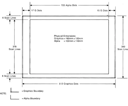
- Built-in high-resolution on-screen graphics display (512 x 390)
- High-resolution character display; 9 x 14 dot character cells; upper and lower case
Display enhancements: inverse video, underline, blinking, half-bright, security and all combinations
- Up to two pages of 24 lines x 80 characters of display memory
The HP 150 can display both alphanumeric and graphics on the 9 inch diagonal screen. The alphanumeric display consists of a 27 line by 80 column format. The 25th and 26th lines are used for the screen labeling of function keys (and all are automatically "touchable" through touchscreen), and the 27th line is for system status and error messages. The screen memory stores 2 pages of text. which allows ~ff-screen storage of the display. High resolution characters with true descend~rs are generated in a 9 x 14 dot cell with half-dot shift. The standard display is green character against a black background.
The graphics display has a resolution of 512 dots horizontally by 390 dots vertically. This gives a 1:1 aspect ratio guaranteeing symmetry (that is, circles look like circles). The numeric keypad also serves as the graphics keypad, allowing the customer to turn on and off the alpha display, turn on and off the graphics display or transfer the graphics display to one of the HP
Introduction
Keyboard
- Detachable, typewriter-style - Special editing keys
- Numeric/Graphics pad
- Eight screen-labeled function keys
The UP 150 keyboard is designed to provide a familiar interface to the system and minimize training time. The low-profile keyboard shape, the sculptured keycaps and the dished "home" keys help to make the keyboard comfortable to use. The 107-key keyboard contains the full local editing keys such as cursor control keys, display scrolling keys, "next" and "prev" keys for scrolling by pages and "insert" and "delete" keys for inserting or deleting characters or entire lines.
Series 100 function keys are screen labels used by the system and by application programs to increase the ease of use of the system. With the HP 150, this capability is enhanced by the use of HProuch. Now, all function keys can be selected by pressing the key itself or by touching the key label on the screen.
Communications/Peripherals
- One RS-232/RS-422 communication port - One RS-232 communication port
- One HP-IB port
- Full block mode graphics terminal support
Two RS-232-C ports (one of which is capable of RS-422 c,ommunication) may be used to connect the system to a remote computer or to serial devices (such as printers or plotters). Flexible protocols allow the use of either hardware or software handshaking and communication speeds can range from 110 to 19,200 baud.
~H_A_R_D_W_A_R_E_O_V_E_R_VI_E_W
________
~[!J
Introduction
Product Specifications General Description Physical Specifications Environmental Conditions Product Regulations Power Requirements Communications
Subsystem Power Requirements
CONTENTS
HP 150 Printed Circuit Assemblies Analog Boards
Power Supply PCA. Sweep PCA.
Digital Logic Boards Processor PCA.
Keyboard PCA.
Mezzanine Memory PCA. RS232C/422 Datacomm PCA. Front Plane PCA.
Video PCA.
Touchscreen PCA.
Hardware Overview
INTRODUCTION
The HP 150 digital hardware performs the logic functions of a 16 bit personal computer with screen graphics. It consists of a Processor PCA, a Memory PCA, a Video subsystem PCA, a Touchscreen PCA, a Front Plane peA, and a Keyboard peA wi thin the Keyboard itself. Its operation is based on the 8 MHz 8088 microprocessor.
The Processor PCA provides control signals, input/output and data processing functions. The 'ROM/RAM PCA provides 256K bytes of dynamic RAM for system and user memory and up to 160K bytes of ROM. The Video subsystem PCA controls the display RAM and provides video display data and timing signals for driving the sweep circui try. The Touchscreen PCA provides an easy user interface to the system beyond the standard keyboard. Two accessory slots are provided allowing for memory expansion and additional processing and I/O capability.
PRODUCT
SPECIFIC A
TIONS
General Description
System Processor:
Main Memory:
Screen Size: Alphanumeric Graphics
Screen Capacity:
Character Generation:
Character Size:
Character Set:
Cursor:
Intel 8088 microprocessor operating at 8 MHz
256K bytes of RAM memory
9 inch diagonal
116 X 150 mm (4.5 X 5.9 inches) 120 X 160 mm (4.7 X 6.3 inches)
24 lines X 80 columns, 25th and ?6th lines for labeling of
function keys, 27th line for system status/error messages.
7 X 10 enhanced dot matrix with 1/2 dot shifting, 9 X 14 dot character cell, nonillterlaced raster scan.
1.3 X 2.8 mm (0.05 X 0.11 inches)
Roman8, line drawing, math standard (also bold and italic usable by applications only)
Display Enhancements:
Refresh Rate:
Tube Phosphor:
Implosion Protection:
Keyboard:
Physical Specifications
Inverse video, underline, blinking, half-bright, security, and all combinations.
60 Hz
P31 (green)
Tension band
Full ASCII code keyboard, eight screen-labeled function keys,
auto-repeat, N-key rollover, cursor controls, 18 key numeric pad,
detachable with 2.43 m (8 ft.) coiled cable.
System Processor Weight: 10.15 kg (22.34 lbs.)
Keyboard Weight: 2.14 kg (4.7Ibs.)
Display Monitor 305 mm
(w)
X 305 mm (D) X 287 mm (H)Dimensions: [12.0 in. X 12.0 in. X 11.3 in. ]
Keyboard Dimens ions:
Flat
Standing
Environmental Conditions
456 mm
(W) X
225 mm (D)X
35 mm(H)
[18.0 in. X 8.9 in. X 1. 4 in. ]456 mm (W) X 225 mm (D) X 35 mm (H)
[18.0 in. X 8.9 in. X 2.5 in. ]
Temperature (Free Space Ambient):
Non-operating Operating
With 2674A (Integral Thermal Printer)
Humidity:
*Vibration:
*Shock
-40 to +75 C (-40 to +167 F)
o
to +50 C (+32 to +131 F)o
to +50 C (+32 to +131 F)5 to 95% noncondensing
5-55 Hz
@
0.015" displacementHardware Overview
*TYPe
tested to qualify for normal shipping and handlingoriginal shipping carton.
Product Regulations
This product when used with HP approved options and peripherals meets the requirements of the following agencies/standards for EDP equipment or office equipment in the following countries:
Safety:
RFI:
Datacomm:
Power Requirements
Input Voltage:
Power Consumption:
45610A 45650A 45655A 45660A
Communications
Data Channels: HP-IB Channel:
RS-232 Channel: Data Rate (RS-232):
Canada - CSA Certification
International - IEC 380/435 Compliance United States - U.L. Listing
Finland - FEI (pending) Germany - VDE Class B
United States - FCC Level B
CCITT v.24 interchange v.28 electrical Australia - Telecom (pending)
Belgium - Prr (pending) Finland - PTT (pending) Germany - FTZ (pending) Sweden - PTT (pending) U. K. - BT (pending)
115 V (+10%,-25%) at 50/60 Hz (+-5~)
230 V (+10~,-25~) at 50/60 Hz (+-5~)
240 Volt Amp
356 Volt Amp 356 Volt Amp 356 Volt Amp
1 HP-IB, 1 RS-232/RS-422, 1 RS-232
Bus used only for specified HP peripherals General asynchronous communications
Port 1 and 2:
Port 1, only:
EIA standard RS-232-C and CCITT v.24; hardware and XOH/XOFF handshaking available.
RS-422 communication capability
Subsystem Power Requirements
The figures below are the worst case power consumption figures for the main system boards. The values given for accessory slots are obtained by subtracting the main system board power consumption figures from the power available from the power supply printed specifications. A more realistic set of-figures for accessory hardware board designers to use in determining power available for accessories is given in Section 3.
PCA +5 Volt +12 Volt -12 Volt
Sweep Board: 125 mA 1.9 A 60 mA
Processor: 2.3 A 140 mA 80 mA
ROM/RAM: 1.0 A 0 0
Video subsystem: 3.4 A 0 0
Front plane: 15 mA 0 0
Thermal Printer: 800 mA 2.2 A
*
0Touch Screen: 0 150 mA 20 mA
Mezzanine Dat~~~mm: 200 mA 50 rnA 50 mA
Accessory Slots: 1.15 A 280 mA 210 mA
TOTAL 9.6
A
2.5 A**
480
mA*
This current at +12v for the TPM comes from a separate winding on the power supply.Hardware Overview
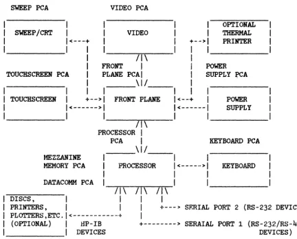
HP 1 50 PRINTED CIRCUIT ASSEMBLIES
The HP 150, in its standard configuration consists of seven modules. They are the Processor, Video, Sweep/CRT, Touchscreen, Keyboard, Power Supply, and Front Plane. Below is a block diagram of the HP 150 system showing each of the modules and their associated PCAs.
SWEEP PCA
SWEEP/CRT
VIDEO PCA
I
I
I
VIDEOI
1<---+
+-->1
OPTIONAL
THERMAL
PRINTER
_ _ _ _ _ 1 I I 1 _ _ _ _ _
I
/1\
I
I
FRONTI
I
POWERTOUCHSCREEN PCA
I
PLANE PCAI
I
SUPPLY ~ATOUCHSCREEN
I
___
\1/__
I
I
I
I
I
I
I
+-->1
FRONT PLANE1<--+
I
1<--->1
1<---1
POWER SUPPLY- - - 1
1---r1rr---1
1
_ _ _ _
_
/1\
MEZZANINE
MEMORY PCA
PROCESSOR
I
PCA
I
_ _ _
\ 1 / _
-PROCESSOR
KEYBOARD PCA
I
I
1<--->1
KEYBOARDI
I
--rrr~Tr~n-1
1---/1\ 1---/1\
/1\
DATACOMM PCA
DISCS,
I
I
I
PRINTERS,
I
I
I
+---> SF.RIAL PORT 2 (RS-232 DEVICES) PLOTTERS ,ETC.1<---+
I
(OPTIONAL)
I
HP-IB+--->
SERAIAL PORT 1 _ _ _ _ _ _ 1 DEVICESFigure 2-1. HP 150 ~ lock Diagram
(RS-232/RS-422 DEVICES)
[image:31.617.67.499.219.567.2]Analog Boards
POWER SUPPLY peA. The power supply used in the HP 150 system is a 120 watt switching supply that provides +5, +12, and -12 volts to the system components. The supply is mounted vertically to the side of the metal chassis and supplies power to the system through a cable which connects to the front plane board and a separate connector on the power supply connects to a ribbon cable to provide +12V to the optional thermal printer (TPM). An overview of the supply is provided in Section
3.
SWEEP peA. The sweep electronics (assembly 45600-60004) used for HP 150 is the same sweep used in the HP 120 computer system. This board also mounts vertically to the side of the metal chassis and interfaces to the digital logic on the video board via a ribbon cable to the front plane board. This sweep provides focus, brightness, vertical and horizontal centering controls at the rear of the uni t. Coarse brightness. horizontal width and vertical size controls are accessible after removal of the shroud of the system. Details about this board as well as the yoke and CRT are found in Section
3.
Digital Logic Boards
There are six PCAs containing primarily digi tal logic which create the HP 150 hardware personality.
Hardware Overview KEYBOARD PCA. The keyboard is detached from the HP 150 unit and a cable connects it to a 6 pin phone jack on the processor board. See Section 3 for more keyboard information.
MEZZANINE MEMORY PCA. The mezzanine memory board (45611-60006) is one of two boards mounted on the processor board in a mezzanine position beneath the video board. The memory board contains ROM, dynamic RAM, CMOS RAM, and indicator LEDs. A 60 pin connector is used to interface the memory and processor boards. See Section 3 for detailed memory board information.
RS232C/422 DATACOMM PCA. The RS232C/422 board (45611-60015) is the other board in a mezzanine position. It connects to the processor board through a 30 pin connector. The board has provision for both asynchronous and synchronous communications and can meet RS232C or RS422 communications standards. Details on this board are in Section
3.
FRONT PLANE PCA. The front plane board (45611-60005) provides the interconnect for the processor, video, touchscreen, sweep, TPM, and accessory boards. The front plane also serves as a conduit for power to the various PCAs from the power supply. Section 3 describes the front plane in more detail.
VIDEO PCA. The alphanumeric and graphics displays are generated by the video subsystem, the core of which is the video board (45611-60003). The video board design is based on an SMC9007 display controller and a custom 40 pin gate array for generation of the alpha and graphics displays respectively. This board is covered in Section 3.
HARDW ARE SUBSYSTEMS
~
______________
~[IJ
CONTEWTS
Front Plane
Thermal (Integral) Printer Interface Front Plane Connectors and Signals Video Board Front Plane Connector Accessory Front Plane Connectors Sweep Board Connector
Touchscreen Connector Integral Printer Connector Power Supply Connector
Front Plane Signal Descriptions Processor Subsystem
OVerview
Memory and I/O Mappings
Processor Board Block Diagram
Reset, CMOS Power, and Test Strap Logic Reset Logic.
CMOS Power Circuit. Test Strap Logic.
Microprocessor System Architecture Bus Cycles
System Timing and Control Logic Clock Generator.
Wait State Generation. GO Generator.
Inte~t Controller I/O ~--"ices
I/O Decoding.
Keyboard and Touchscreen Controller. Datacomm.
HP-IB Controller and Interface. Real Time Clock.
Video Subsystem
Video Technology and Display Format Raster Scan.
Video Frame Format. Alpha Screen Format.
Displaying Alpha Characters Alpha Character Cell Format. Alpha Video Enhancements. Graphics Display.
Video Board OVerview
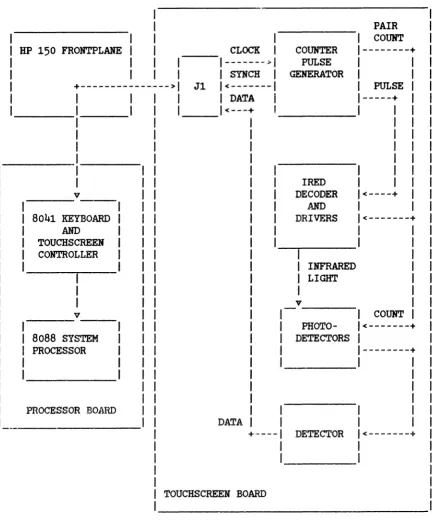
Keyboard and Touchscreen Subsystem Keyboard
Electrical Interface. Keyboard Operation. Touchscreen
Mechanical Description. Specifications
Timing
Interface Description.
Resolution Versus Humber of Pairs.
Pair Address to Row, Column Ho. Conversion. 8041 Keyboard/Touchscreen Scanner
Block Diagram.
Status Register (I/O Port 0019H). Initialization.
8041 Commands (I/O Port 0019H).
Keyboard and Touchscreen Data Input (I/O Port 0018H). Datacomm Subsystem
General Description
RS232C/422 Datacomm Module Connector Baud Rate Generator
Multi-Protocol Controller
Communications Interface Circuitry Mezzanine Memory Subsystem
Mezzanine Memory PCA PCA Overview
Connector Signals ROM
ROM Decoding.
Wait State Disable. ROM Timing.
Slot Selection Generation CMOS RAM
CMOS Decoding and Access. CMOS Power.
LIDs
LED Decoding.
LED Register Reset. Dynamic RAM
Decoding.
Dynamic RAM Refresh. PCA Configuration. Accessories Subsystem
Accessory Hardware Design Guidelines Mechanical Specifications
Power Requirements Thermal Limits
Accessory Signal Loading Restrictions Signal Timing Diagrams
Accessory Front Plane Connector
Accessory Connector Signal Descriptions Accessory Card Hardware and Electrical
Electrical Design Helpful Design Hints
General Schematic Discussion Tranceiver Schematic Discussion Mechanical Design
Helpful Design Hints I/O Panel Design List of Vendors
Hardware Subsystems
FRONT PLANE
The front plane, or mother board, of thE:' HP 150 svstem is the board that provides the interconnection of the various components of the system. The processor, video, and two optional accessory boards plug into connectors on the front plane. Four cable connectors interface the power supply, sweep, touchscreen, and optional TPM to the rest of the system via the front plane. The front plane is used primarily to provide a comnnmications path from the processor board to the video and accessory boards. Tb ... r'e is some digital logic on the front plane which is used for transferring bytes from the processor to the TPM. This circuitry is described below. Power for each of the boards comes from the power suppply via the front plane. Video signals are transmitted to the sweep via the front plane and timing signals for the touchscreen are transmitted or received via the front plane.
Thermal (Integral) Printer Interface
The optional thermal printer mechanism (TPM) interfaces to the rest of the system via logic on the front plane and processor boards. The processor sends a data byte to the TPM by writing the byte into a transparent latch on the
front plane. A negative going pulse on NTPMWRT is sent causing the latch to receive the data byte. On the positive edge of NTPMWRT (the deassertion of NTPMWRT) the byte is latched into the latch. Also, a D flip-flop on the front plane is clocked which results in NSTR (JF7-15) being asserted (goes low). The assertion of NSTR tells the TPM that a byte is available for it to read. After the TPM reads the byte in the latch, it asserts NACK (JF7-6) by bringing it low. This results in the flip-flop preset inputs going low presetting the two D flip-flops. This makes NSTR go back high in preparation for the next byte to be sent to the TPM by the processor. It also makes the output of the D flip-flop go low which in turn makes NOCINT go low. NOCINT is one of the open collector interrupt lines on the front plane. Asserting NOCINT causes an interrupt to the processor. The interrupt service routine will poll the devices which assert NOCINT to determine which device to service. After receiving an interrupt from the T~ interface logic, the 8088 can send another byte to the TPM. (Note that an interrupt service routine must poll the TPM interface logic last because the poll consists of reading the TPM status which also clears the interrupt at the end of the poll.)
A read or write to the TPM will cause the processor board signal NTPMSL to go low which results in 6 wait states to be added to the bus cycle.
The TPM connects via a ribbon cable to a connector on the front plane. The 8088 accesses the TPM at I/O address XX30 as described in the Memory and I/O Mapping section of this manual. Note that "XX" can be any (address) value.
Summarizing, a byte of data is sent to the TPM by writing the data at port XX30. The TPM acknowledges the receipt of the data and readiness to accept the next byte of data to be sent by asserting the NOCINT interrupt line. The interrupt handling routine can poll the TPM by reading port XX30 and inspecting the least significant bit. If the bit is set, the TPM has generated an interrupt. The end of the read cycle clears the interrupt if caused by the TPM. PAPER OUT and ONLINE status are also available at the same address.
Front Plane Connectors and Signals
The following paragraphs provide a description of the connectors and the connector signals on the front plane.
Front Plane PCA Connector Layout:
JF5 -SWEEP
JF6
-TOUCHSCREEN
I
I
I
I
JFl - VIDEO BOARD
JF2 - PROCESSOR BOARD
JF7-INTEGRAL
PRINTER
I
I
I
I
I
JF3 - ACCESSORY SLOTl
JF4 -
ACCESSORY SLOT2JF8
Hardware Subsystems
JF2 - Processor Board Front Plane Connector Pinouts and Signals
1. FPA 0 33. NTPMWRT 65. NTPMRD
2. FPA 1 34. NPFAIL 66. GND
3. FPA 2 35. NSLOTSEL 2 67. GND
4. FPA 3 36. FPNRST 68. +5V 5. FPA 4 37. NOCINT 69. GND
6. FPA 5 38. NOCWAIT 70. +5V
7.
FPA 6 39· +5V 71. GND8. FPA 7 40. BIO/-M 72. GND
9· ABUS 8 41. -12V 73. GND 10. ABUS 9 42. NVIDINT 74. GND
11. ABUS 10 43. -12V 75· GND
12. ABUS 11 44. FPGO 76. GND
13. FPA 12 45. GND 77. GND
14. FPA 13
46.
GND 78. GNO15· FPA 14 47. FPCLK 79· GND
16. FPA 15 48. GND 80. GND
17. FPA 16 49. GND 81. GND
18. FPA 17 50. BIO/-M 82. GND
19· FPA 18 51. +12V 83. GND
20. FPA 19 52. FPDT/-R 84. GND
21. FPD 0 53. +12V 85. GND 22. FPD 1 54. SHOLDA 86. GND
23. FPD 2 55· FPNWRT 87. GND
24. FPD 3 56. N.C. 88. +5V 25· FPD 4 57. FPNRD 89. +5V
26. FPD 5 58. +5V 90. +5V
27. FPD 6 59. N.C. 91. +5V 28. FPD 7 60. GND 92. TSDATA 29· FPNSSO 61. TSCLK 93. GND
30. NSLOTSEL1 62. GND 94. NDCOCINT
31. BATV 63. N.C. 95· TSSYNC
32. BATV 64. FULLMEM 96. +5V
JF2
+--- ---+
32
I
+ +...
•.. + +I
164
I
+ +...
.•• + +I
3396
I
+ +...
... + +I
65+---+
Video Board Front Plane Connector
JFl - Video Front Plane Connector Pinouts and Signals
1. FPA 0 2. FPA 1
3. FPA 2
4. FPA 3 5. FPA 4
6.
FPA5
7. FPA 6
8. FPA 7 9. ABUS 8
10.
ABUS 911.
ABUS10
12.
ABUSll13.
FPA12
14. FPA
13
15.
FPA 1416.
FPA15
17. FPA 16 18. FPA 17 19. FPA 1820.
FPA 19 21. FPO 0 22. FPD 123.
FPD 224.
FPD3
25.
FPD 426.
FPD 527. FPD 6 28. FPD 7
29.
+5V
30.
+5V
31.
+12V
32.
+12V
33.
+12V
34. BATV
35.
BATVJFl
36. +5V
37. GND
38. FPNRST
39. GND
40. NOCWAIT
Jll.
+5V
42.
BIO/-M
43. GND
44.
NVIDINT
45.
GND46. FPOO
47. GND
48. FPCLK
49. GND
50. +5v
51.
GND52. BIO/-M
53.
GND54.
FPDT/"'R55. N. C.
56. +5V
57.
N.C.58. FPNRD
59.
GND60.
(RESERVED)61. GND
62. +5v
63.
GND64.
NVSYNC
65. GND 66. NHSYNC
67. GND 68. WB
69. NFB
70. GND
+---+
35
I
+ + ...
. .. +
+I
1
70
I
+ + ...
. ..
+ +I
36
+---+
Hardware Subsystems
Accessory Front Plane Connectors
The accessory boards plug into the bottom slots of the card cage. The system signals available to the modules are listed below.
JF3/4
Accessory Board Front Plane Connector Pinout and Signals1-
FPA0
36.
(RESERVED)*
2.
FPA1
37.
NPFAIL3.
FPA2
38.
(RESERVED)*
4.
FPA3
39·
FPNRST5·
FPA4
40.
+5V
6.
FPA5
41.
GND7.
FPA6
42.
GND8.
FPA7
43.
NOCINT9.
ABUS8
44.
aND10.
ABUS9
45.
NOCWAIT11-
ABUS10
46.
(RESERVED)*
12.
ABUS11
47.
BIO/-M13.
FPA12
48.
+5V
14.
FPA13
49.
-12V
15.
FPA14
50.
NDCOCINT16.
FPA15
51-
aND17.
FPA16
52.
-12V
18.
FPA17
53.
SHOLDA19·
FPA18
54.
FPGO20.
FPA19
55.
+5V
21-
GND56.
GND22.
GND57.
FPCLK23.
FPD0
58.
(RESERVED)*
24.
FPD1
59.
GND / FULLMEM*
25·
FPD2
60.
+12V
26.
FPD3
61-
GND27.
FPD4
62.
BIO/-M28.
FPD5
63.
+12V
29.
FPD6
64.
FPNWRT30.
FPD7
65.
+5V
31-
GND66.
FPTYr/-R32.
FPNRD67.
GND33.
GND68.
FPNSSO34.
+5V
69.
GND35·
BATV70.
NSLOTSELx**
JF3
andJF4
+---+
35
I
+ +
...
.
..
+ +
I
1
70
I
+
+...
.
..
+ +
I
36
+---+
*
Pin 59 is FULLMEM is on JF3 only. Pin 59 is GND on JF4.Connections to this pin and all pins labeled RESERVED should not be made.
**
HSLOTSELx will be either HSLOTSEL1 or HSLOTSEL2 depending upon which s ide of the front plane the module is plugged into. The left s ide of the card cage (from rear view of the package) holds module 1 and gets the NSLOTSEL1 signal. The right side of the card cage holds module 2 and gets HSLOTSEL2.Sweep Board Connector
The Sweep board connects to the front plane via a 20 pin connector, JF5, whose signal pins are listed below:
+---+
20. + + 10. 20. +5V 10. NHSYNC
+ + 19. GHD 9· +12V
+ +
lB.
NHBB.
GND+ + 17. GND 7. +12V
+ + 16. NFB 6. GND
+ + 15. GHD 5. +12V
+ + 14. SWPNRST 4. GND
+ + 13. -12V
3.
GND+ + 12. +12V 2. +12V
ll. + + 1. ll. HVSYHC 1. +5V
+---+ JF5
Touchscreen Connector
The Touchscreen connects to the front plane via a 10 pin connector, JF6, whose signal pins are listed below:
+---+
1. + + 6. 1. +12V
6.
+12V+ + 2. TSDATA 7. +12V
+ +
3.
-12VB.
GND+ + 4. TSSYNC 9. TSCLK
5· + + 10. 5· GND 10. GND
Hardware Subsystems
Integral Printer Connector
The Integral Printer connects to the front plane via a 20 pin connector.
JF7. whose signal pins are listed below.
+---+
l. + + l l . l. DO ll. D1
+ + 2. D2 12. D3
+ +
3.
D4 13. D5+ + 4. D6 14. D7
+ + 5· NPOR 15· NSTR
+ + 6. NACK 16. POUT
+ + 7. N.C. 17. NONL
+ + 8. GND 18. GND
+ + 9. +5V 19· +5V
10. + + 20. 10. N.C. 20. N.C.
+---+
JF7
Power Supply Connector
Power to the system comes from the power supply through a 12 pin connector. JF8. on the front plane board. The signal definition is given below:
+---+
l. + NPFAIL
(Pin removed for polarization)
3. + GND
4.
+ -12V5· + GND
6. + (N. C. )
7.
+ +12V8. + GND
9· + +5V
10. + +5V
11. + +5V
12. + GND
+---+ JF8
Front Plane Signal Descriptions
The following description of the front plane signals referenceche connector diagrams shown previously.
FPA 0-7
ABUS 8-11
The lower 8 address bits of the 20 bit address generated by
FPA 12-19
FPDBUS 0-7
FPCLK FPNRD FPNWRT FPNSSO BIO/-M FPDT/-R FPGO HOCWAIT NVIDINT lIDCOCINT NOCINT
These signals also are buffered and demultiplexed.
Data bus signals from the external data bus. This data path is the means through which data is passed between the processor and the video board or option slot modules or the optional TPM.
Buffered 8 Mhz system clock.
Buffered -RD signal from the 8088 used to indicate a bus read cycle in progress.
Buffered -WRT signal from the 8088 used to indicate a bus write cycle in progress.
8088 bus cycle status line. The combination of FPNSSO, BIO/-M, and FPDT/-R allow boards connected to the front plane to completely decode the current bus cycle.
Buffered IO/-M signal from the 8088 used to distinguish memory wld I/O bus cycles.
Buffered DT/-R signal from the direction of data from the 8088 for
8088 used to a given bus cycle.
indicate
Signal which qualifies the address generated by the microprocessor. The address qualification is needed primarily for dynamic RAM circuits which cannot tolerate an assertion of RAS or CAS on a false address. FPGO goes high at the beginning of T2 and goes back low at the beginning of T4 of a bus cycle. FPGO can also be used to terminate a bus wri te cycle by having its falling edge used to clock data into a register or other device on an accessory device in an option slot. Terminating the writes in this way can provide better hold timing than using FPNWRT.
This line can be asserted by the ()ption modules or video board through an open collector gate to insert wait states into a bus cycle to provide sufficient time for a bus cycle access.
This line is asserted by the video subsystem to generate an interrupt to the processor. This interrupt occurs once every frame. The signal can be monitored by the option slot devices if desired.
This open collector interrupt signal has the same interrupt priori ty as the datacolll..l11 controller chip on the processor board as it shares the same input to the interrupt controller as the datacomm controller chip does. This input can be asserted by accessories for interrupt servicing.
System interrupt signal asserted by a device collector gate. This line can be used by options processor service.
SHOLDA
FULLMEM
NSLOTSELl
NSLOTSEL2
NFB
NHB NHSYNC
NVSYNC
TSCLK
TSDATA
TSSYNC
NTPMRD NTPMWRT
FPNRST
NPFAIL
BATV
Hardware Subsystems
Synchronized hold acknowledge signal from the 8088. is asserted by the mezzanine memory board.
HOLD
Indicates which mezzanine memory board option is installed. FULLMEM=O if 128K RAM and FULLMEM=l (it is pulled high by a pull up resistor on an installed extension memory board) if' 256K RAM is on the board. An accessory should not connect to this signal pin.
Signal indicating an address within the 64K block allocated to option module 1 has been generated by the 8088.
Same as NSLOTSELl but asserted when address within option module 2 address space is generated.
Video Full-Bright signal to sweep board.
Video Half-Bright signal to sweep board.
Horizontal sync signal from video board used by the processor and sweep boards.
Vertical sync signal from video to sweep board.
Touchscreen clock signal.
Touchscreen data signal.
Touchscreen sync signal.
Signal from CPU to read TPM status.
Signal generated by the processor card to handshake bytes of' data to the TPM.
Signal generated by processor board at initialize logic circuitry.
power-on time to
Signal generated by the power supply indicating power supply output level stability.
These two connector lines carry located on the video board to back-up power such as the CMOS clock.
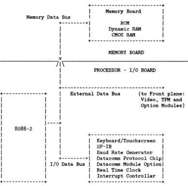
PROCESSOR SUBSYSTEM
Overview
The UP 150 processor board is based on the Intel 8088-2 microprocessor. The microprocessor runs at an 8 MHz clock speed and is configured for operation in the min~ mode. The general architecture of the processor, memory, and I/O is depicted in figure 3-1. As shown in the diagram, the majority of the circuitry is partitioned between three data busses: the memory data bus, the I/O data bus, and the external data bus.
+---+
~lemory Data Bus
+--->1
1
1
1
1
Memory Board
ROM
Dynamic RAM
CMOS RAM 1
1 1
+---+
MEMORY BOARD
v
---~~/I~\---1
1
1
PROCESSOR - I/O BOARD
+--->
+---+
External Data Bus (to Front plane:----+
8088-2 1
Video, TPM and Option Modules)
1
+---+
1 Keyboard/Touchscreen 1
1 IIP-IB 1
1
1
Baud Rate Generator1
+--->1
Datacomm Protocol Chip1
I/O Data Bus 1 Datacomm Module Option 1
1 Real Time Clock 1
1 Interrupt Controller 1
+---+
+---+
[image:48.620.76.465.242.626.2]Hardware Subsystems
Memory and I/O Mappings
The logic on the processor board and the other boards which exchange data with the microprocessor are mapped into the 8088's memory or I/O space. Section 4 depicts the memory and I/O maps for the system. Note that I/O addresses xx80 through XXFF are available for option module use. Also note that "XX" can be any value.
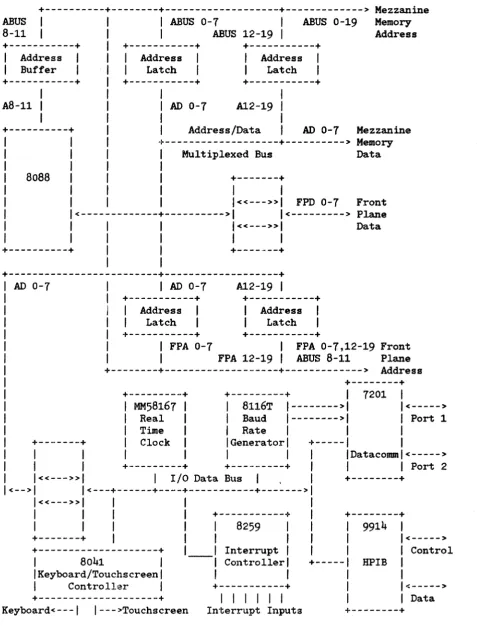
Processor Board Block Diagram
+---+---+---+---> Mezzanine
ABUS 1
I
ABUS 0-7 1 ABUS 0-19 Memory8-11 1 1 ABUS 12-19 1 Address
+---+ +---+ +---+ Address Buffer Address Latch Address Latch +---+ +---+ +---+ 1
A8-11 1 1 1 AD 0-7 A12-19 1 1
1 1 I
+---+ 1 Address/Data 1 AD 0-7 Mezzanine
1
1 1
8088 1
I
1
1<----1
1
+---+---> Memory
1 Multiplexed Bus Data
1
1 +---+
I
1 1«---»1 FPD 0-7 Front
---+--->1 1<---> Plane
1 1«---»1 Data
1 1 1
+---+ 1 +---+
I
+---+---+
I
AD 0-7I
AD 0-7 A12-19I
+---+ +---+ Address Latch +---+ Address Latch +---+ +---+
I FPA 0-7 I FPA 0-7,12-19 Front
1 FPA 12-19 1 ABUS 8-11 Plane
+---+---+---> Address +---+ +---+ MM58167 Real Time Clock
+---+ 1 7201
I
8116T 1--->1 1<---> Baud 1--->1 1 Port 1
1 Rate 1 1 1
1 Generator 1 +---1 1
I
1I
1 Datacomm 1 <--->+.---+ +---+ 1 1 1 Port 2
1 «---» 1 1 I/O Data Bus 1 , 1 +---+
<-->1 1<---+---+----+---+--->1
1«---»1
I
I
I
I
I
1I
+---+I
+---+I
1I
I
8259I '
9914 ,+---+, 1 , , 1<--->
+---+, Interrupt" 1 1 Control
, 8041
I
Controller, +---1 HPIB ,'Keyboard/Touchscreen' ' "
1 Controller 1 +---+ 1 1<--->
+---.---+ 1 , 1 I I
I
I I DataKeyboard<---I I--->Touchscreen Interrupt Inputs +---+
[image:50.615.65.543.58.687.2]Hardware SubsysteDb
Reset, CMOS Power, and Test Strap Logic
This set of miscellaneous circuits provide functions of an ancillary or support nature to the more visible functions of the board to be described later.
RESET LOGIC. The power-fail signal from the power supply (NPFAIL, Jl-34) is used
b.Y
the system as a power-on-reset and a CMOS device standby operation mode switch. NPFAIL is low when power is first applied to the system and goes high no sooner than 75 msec after the power supply output voltages have stablized at their specified values. When NPFAIL goes low due to the power being disconnected from the power supply, it does so at least 500 usec before the power supply output voltages go out of regulation.CMOS POWER CIRCUIT The CMOS power circuit regulates current use
b.Y
real time clock and configuration CMOS memory between the batteries and the power supply while the unit is switched on.TEST STRAP LOGIC. If the test strap input is held low during execution of manufacturing self-test, a failing test will be iterated until the failure ceases or the input is brought high. This is intended to be a convenience for servicing purposes.
Microprocessor System Architecture
BUS CYCLES
Address Generation. At the beginning of a bus cycle (memory or I/O access), the 8088 places the memory or I/O address on its address and address/data pins. The address is multiplexed with the data and some of the status information so the processor board uses transparent latches to latch and buffer the address generated at the beginning of the cycle. Address bits A8-Al1 are not multiplexed so a non-latching buffer is used for buffering those four signals. ALE (U211 pin 25) is the signal used to latch the address into the latches.
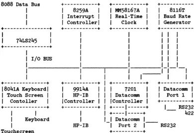
Data Transactions. The 8088 does all data transactions through one of three bus tranceivers. All the mezzanine memory board components are isolated by a transceiver located on the memory board. All the I/O devices (real time clock, datacomm, baud rate generator, keyboard/touchscreen controller, HP-IB
controller, etc.) are on the I/O bus which is separated from the 8088 by another transceiver on the processor board. Any access not to the mezzanine memory or the I/O bus will default to the front plane.
Status Generation. The 8088 generates status information indicating the type of bus cycle in progress. Control signals based upon these are generated by the processor and are buffered and sent throughout the system to allow circuitry to respond properly to read, write, memory, or I/O cycles.
HOLD State. The 8088 will be put into a HOLD state by the mezzanine memory approximately every 56 usec during dynamic RAM refresh.
System Timing and Control logic
CLOCK GENERATOR.. The 8284A clock generator is used to provide the system clock for the HP 150 hardware. A 24 Mhz crystal provides the reference frequency used by the 8284. The 8284 creates an 8 MHz clock which nominally is high 33~ and low 66% of the 125 nsec period. The 8284 also divides the 8 Mhz clock by 2 to form the 4 Mhz signal ui3ed as the system clock for the 7201 datacomm controller, the 8116T baud rate generator, the 9914A HP-IB controller, and the 8041A keyboard and touchscreen controller.
The 8284 also provides a reset output pin which is used as a basis for the reset signals throughout the system hardware.
The -F/C input (pin 13) of the 8284 is at a logic 0 state which selects the crystal oscillator as the source frequency for the 8284.
Hardware Subsystems
WAIT STATE GENERATION. The basic bus cycle for the 8088 consists of four 125 nsec clock periods during which the memory of I/O address is generated by the CPU followed by a transmission of data to or the reception of data from a memory or I/O device. The cycle can be extended by adding "wait states" to the basic 4 clock cycle. The standard bus cycle is shown in figure 3-3.
CLK
(8
Mhz)ALE
READY
1<--
T1--->1<--
T2--->1<--
T3--->1<--
T4--->1
\I
---_/
\I
\ _
-Figure 3-3. Standard Bus ~ycle with no Wait States
The four clock periods are labeled T1 through T4 for reference purposes. The 8088 samples the READY input during the low clock period of T3. If it is high at that time, no extra wait states are added. If it is low, a wait state is added as shown in figure 3-4. READY is sampled during the low clock period of every wait state. Whenever it is sampled high, the wait state is exited and the bus cycle goes into the T4 state.
-- T2
-->1<--
T3--->1<--
TW--->1<--
TW--->1<--
T4--->1
CLK
(8
Mhz)--\
/
READY __ /\ _ _ _ _ _ _ _ _ /
\/
\ _
-Figure 3-4. Bus Cycle with Two Wait States
The READY input to the 8088 is driven by the ROY output (pin
5)
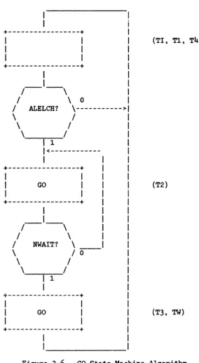
of the 8284. The 8284 has two inputs, RDY1 and ROY2 (pins 4 and 6), by which uai t states are controlled. Normally, wait states are added by RDY1 (NWAIT). RDY1 is sampled at the falling edge of each clock, so effectively, the READY input of the 8088 is controlled by what the 8284 samples at its RDY1 input just prior to the beginning of T3 or just prior to the beginning of each wait state.A min~ of one wait state is added to every bus cycle when jumper W1 is installed. (Access of devices requiring more wait states get the additional wait states needed but one wait state appears in bus cycles on accesses of devices whose decoding logic isn't tied into the wait state generator.) Installing W2 causes no wait states to be added for ROM access only.
Wait states may be inserted by other logic boards by
line that is routed to the front plane option slots and
As long as NOCWAIT is low, wait states will be executed the NOCWAIT input goes into a synchronizing flip-flop by an option or the video board must be anticipated The timing diagram in figure 3-5 illustrates wait state by an option card.
asserting the NOCWAIT video board connector.
by the 8088. Since the wait states added in a timely fashion.
insertion and deletion
1<---
T2-->1<--
T3--->1<--
TW--->1<--
TW--->1<--
T4--->1
CLK