Elrawemi, Mohamed, Muhamedsalih, Hussam, Blunt, Liam, Fleming, Leigh, Martin, Haydn and
Jiang, Xiang
Comparative study between online and offline defect assessment methods for roll to roll flexible PV
modules
Original Citation
Elrawemi, Mohamed, Muhamedsalih, Hussam, Blunt, Liam, Fleming, Leigh, Martin, Haydn and
Jiang, Xiang (2014) Comparative study between online and offline defect assessment methods for
roll to roll flexible PV modules. In: 4th International Conference on Nanomanufacturing
(nanoMan2014), 810 July, Bremen, Germany.
This version is available at http://eprints.hud.ac.uk/id/eprint/21210/
The University Repository is a digital collection of the research output of the
University, available on Open Access. Copyright and Moral Rights for the items
on this site are retained by the individual author and/or other copyright owners.
Users may access full items free of charge; copies of full text items generally
can be reproduced, displayed or performed and given to third parties in any
format or medium for personal research or study, educational or notforprofit
purposes without prior permission or charge, provided:
•
The authors, title and full bibliographic details is credited in any copy;
•
A hyperlink and/or URL is included for the original metadata page; and
•
The content is not changed in any way.
For more information, including our policy and submission procedure, please
contact the Repository Team at: [email protected].
8 – 10 July, 2014,Germany
Comparative study between online and offline defect assessment methods
for roll to roll flexible PV modules
*M. Elrawemi1, H. Muhamedsalih1, L. Blunt1 L. Fleming1 H.Martin1 and X. Jiang1
1 Centre for Precision Technologies, University of Huddersfield, HD1 3DH, Huddersfield, UK
*corresponding author (email: [email protected] ;)
ABSTRACT:
Flexible PV modules are manufactured using roll to roll (R2R) technology. These modules require a flexible barrier material to prevent water vapor ingress. The basic methodology to produce such barriers is to combine oxide layer (e.g. AlOx) coating with suitable polymer substrates. However, micro and nano scale defects can
appear at any stage of the coating process thus affecting the module efficiency and lifespan. To guarantee the barrier properties, surface inspection needs to be carried out during the manufacturing process. In the present study a stabilised in-line detection system based on wavelength scanning interferometry (WSI) has accurately and reliably captured defects down to 3um in lateral dimension. The main aim of this research paper is to compare results of coherence correlation interferometry (CCI) as an offline technique with WSI results for detecting PV barrier film defects. The results show the capability of the WSI to be implemented in the manufacturing environment for defect detection in roll to roll manufacture.
Keywords
:
Quality assurance, Coating, Metrology and R2R.1
Introduction
This paper reports on the recent work carried out as part of the EU funded NanoMend project. The project seeks to develop integrated process inspection, cleaning, repair and control systems for thin films on flexible PV films. Thin-film solar cells based on Copper Indium Gallium Selenide (CIGS) materials are being considered for large scale power generation as well as building integrated photovoltaic (BIPV) applications. Since CIGS cells are very sensitive to moisture, they must be effectively encapsulated in order to satisfy the international standard IEC 61646 which requires the efficiency to degrade less than 10 % after 1000 hours in an environment of 85 ºC and 85% relative humidity [1]. Thin Al2O3 film
deposited via atomic layer deposition (ALD) techniques on polymer substrates have been shown to have the potential to reduce moisture permeation to a WVTR of 5x10⁻⁶ g/m2/day at room temperature [2], which should protect CIGS cells. The ALD is currently being developed for continuous R2R processing. This development is significant because R2R processing would allow ALD to address many applications in a cost effective manner. However, defects appearing on the film surfaces during the Al2O3 growth have been seen to
be highly significant in deterioration of the PV module efficiency and lifespan. Therefore, an on-line inspection system needs to be implemented to optimise the production process for coated polymer
film. This research paper provides a performance comparison study between in-line wavelength scanning interferometer (WSI) and off-line coherence correlation interferometer (CCI) to detect micro scale defects. This is done in order to verify the applicability of WSI.
2
Flexible PV Barrier Film Defects
[image:2.595.330.507.570.744.2]Small individual defects such as particles or pinholes are generally caused by particulate contamination or the surface roughness of the substrate. Figure (1) shows a particle defect in 125 um thick planarised Polyethylene Naphthalate (PEN) layer before Al2O3 ALD coating.
8 – 10 July, 2014,Germany
These defects are believed to be critical features limiting the performance of gas diffusion barriers, as they can mask the polymer substrate and prevent Al2O3 ALD coating. These particles then move or
are dislodged after the Al2O3 ALD coating process
and leave an uncoated region of the polymer substrate resulting in high water vapor ingress. In figure (2) the SEM pictures show evidence of typical defects which are caused by the effect of a dust-contaminated substrate surface [3].
[image:3.595.73.279.307.481.2]The left pictures show the morphology of a defect where particles are detached after the coating. This leaves a hole in the coating with a crater-like shape where the centre remains uncoated. The right two pictures in figure (2), show dust particles which are still attached to the surface. They are coated with the same layer thickness as the substrate which is too small to completely cover them. These defects can be avoided by substrate preparation and by depositing the coatings in a dust-free environment.
Fig. 2: Typical barrier layer defects pin holes and attached particles [3]
As no barrier coating technology is perfect, coating related defects have to be inspected and controlled to assure high-yield manufacturing.
2.1 Defect Detection and Characterisation
It is impossible for non-microscopic methods to observe defects at the micro and nano scale, which may appear at any stage of the barrier films coating process. Therefore, it is desirable to have a technique available which quickly measures, at a micro/nano scales, the properties of the coating layer during the stages of barrier layer production. Conventional surface metrology methods such as, white light scanning interferometry (WLSI) based on coherence correlation interferometry (CCI) technique is mostly used as an offline technique for quality control providing a means of characterising a number of important 3D areal parameters; including surface roughness, defects density and defects size scale, which have a large influence upon the efficiency and lifespan of the PV solar
module. However, the thickness, growth, conformality and the degree of coverage of the extremely thin (20-80nm) Al2O3 layer can be best
imaged with scanning electron microscopy (SEM). The technique provides visual information on surface features with lateral resolution down to a few nm. However, these techniques are in fact lab based, and are impractical to be used for process control. Therefore; detecting defects off-line has become more difficult and time consuming by these methods. This procedure can often result in large quantities of substrate being manufactured before defects are detected. In addition the quality requirements and line speed are increasing and off-line methods are not efficient to operate within these requirements. Hence, it is desirable to make use of other optical based in-line inspection systems during the R2R coating process so that it is assured that, only completely inspected surfaces that have been found to be of good quality remain to be used for PV encapsulation.
2.2 In process Metrology
To facilitate in process measurement two significant issues need to be addressed; i) the measurement must be fast and non-contact ii) the measurement must be carried out in a “noisy” working environment. Given the general roughness level on the substrate is in the nm range then only optical interferometry can assess the barrier film surface topography.
Unfortunately the interferometric measurement
techniques are extremely sensitive to
environmental noise such as mechanical vibration, air turbulence and temperature drift. Thus, controlling the impact of noise is essential in this application.
Consequently the authors have introduced an environmentally compensated interferometric technique for R2R barrier coating inspection based on the principle of wavelength scanning interferometry (WSI) [4]. The working principle of this technique is shown in figure (3).
[image:3.595.321.527.579.695.2]PI controller B.S PZT Reference mirror Sample Objective lens (5X) SLED Halogen lamp AOTF CCD AOTF driver Edge-pass filter Stabiliser WSI Photo-detector Optical fiber
Fig. 3: Configuration of the WSI [4]
2.3 Wavelength Scanning Interferometry
8 – 10 July, 2014,Germany
R2R barrier coating, it should be capable of performing fast surface measurement and be robust against environmental disturbance. The WSI has these two features. It can perform the essential phase-shifting operations at high speed with no moving mechanical parts while scanning the visible wavelength over a wide spectrum range using an acousto-optic tuneable filter (AOTF).
The dual interferometer paths, produced by multiplexing the scanned wavelength with an infrared light source via a dichroic mirror, allows for compensation of environmental noise by servo control of the reference mirror. A full field of view measurement can be obtained under R2R process conditions within less than a second. Hence the WSI can carry out quantitative measurements of
micro/nano scale surface topographical
characteristics at much higher speeds compared to standard white light coherence scanning interferometers.
3
Experimental work
Exemplar samples of Al2O3 ALD barrier film were
first measured using off-line metrology techniques (CCI) in order to detect and measure the defects and compare them later with the WSI measurement results. The sample used has an 80 mm diameter Polyethylene Naphthalate coated area with 40 nm thick aluminium oxide film. The measurement protocol was as the following, more than 100 measurements carried out by each of the techniques and five different defects were collected from the sample. These defects have a lateral dimension ranges approximately (35-60) um. The region which has been measured by the CCI has also been investigated by the WSI for comparison purposes. Table (1) shows the technical specifications of each technique. The specifications are given for the off-line CCI and in-off-line WSI.
Typically, the lateral range and resolution are varied for different objective lenses and imaging sensor sizes. The current WSI setup has CCD sensor size of 640x480 and objective lenses set of 2X and 5X magnifications. Whereas, the considered CCI sensor size is 1024x1024 pixels with objective lenses set of 5X, 20X and 50X magnifications and working distances shorter than the WSI equivalent objectives. Therefore, the WSI has the potential to increase the lateral range and resolution by simply changing the CCD senor size and objectives.
The table also shows that the vertical range for both instruments are equal, but this value mainly depends on the focus depth of the objective for the WSI. However, in this application, the defects vertical depth does not exceed several micrometres which are within the limit of focus depth of high magnification objectives.
. Table 1. Technical specification
Specifications
Method
CCI
WSI
Area (objective dependent )
0.3-7.2mm2 0.5-1.8mm2
Vertical resolution
0.001 nm 15 nm
Vertical range 100 um 100um
Lateral resolution 0.36 um 2.98 um
Repeatability of surface (noise)
0.003 nm 7 nm
Typical measurement time
10-20 seconds
<1 second
4
Results and Discussion
[image:4.595.312.523.75.227.2]Both systems (CCI and WSI) are calibrated and should yield closely comparable results. The work carried out in this research paper shows that, the surface roughness parameter value for defect free sample measured by the WSI is higher when compared to the CCI method, see figures (4) and figure (5). This is due to the high noise floor level generated during the operation process of the WSI technique. This noise could be generated from accumulative effects of environmental noise and WSI resolution and measurement uncertainty. However, this tolerance in the magnitude of surface roughness does not effect on defect detection ability nor characterisation since the coating thickness is approximately 40 nm.
Fig. 4: Surface roughness measured by the CCI
[image:4.595.326.511.447.572.2] [image:4.595.326.508.593.741.2]8 – 10 July, 2014,Germany
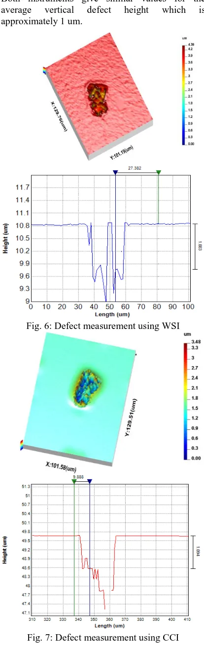
Figure (6) and figure (7) show the same defect which has been measured by both CCI and WSI. Both instruments give similar values for the average vertical defect height which is approximately 1 um.
[image:5.595.71.278.96.756.2]Fig. 6: Defect measurement using WSI
Fig. 7: Defect measurement using CCI
[image:5.595.314.528.175.312.2]A 5X objective lens giving sample spacing of 1.19 um was used in the WSI, and for the CCI 20X objective lens giving sample spacing of 0.9 um was used. More than 100 measurements carried out by each of the techniques. As an initial assessment for WSI measurement, it was found that the results are comparable to the off-line technique (CCI). Example of the defects size/scale captured by the techniques is shown in figure (8).
Fig. 8: Defects lateral size measured offline and online process
The result in the above figure indicates that, the WSI system has accurately and reliably captured defects that have been detected previously by the CCI. The WSI technique can be an efficient and optimal system to be used for in process thin film barrier defects inspection.
5
Conclusion
High quality barrier films are critical if PV manufacturers are to exploit the possibilities offered by flexible large substrate area flexible photovoltaics. The current work has shown that the WSI method can be a quality assurance tool to study the surface topography of the Al2O3 ALD
barrier films defects and results compare
favourably with Coherence Correlation
Interferometry, Scanning Electron Microscopy and Atomic Force Microscopy. This method has the following advantages: it can be used for areal measurement at high speed, < 1 second per full field of view, and it is robust against environmental disturbance. The WSI can be integrated onto R2R platforms as a quality assurance tool.
6
Acknowledgments
The authors would like to thank the EU for providing funds to carry out this work via the NanoMend project NMP4 LA-2011-280581 and the EPSRC for funding the UK Centre for Advanced Metrology.
0 10 20 30 40 50 60 70
defect 1 defect 2 defect 3 defect 4 defect 5
D
e
fe
c
t
la
te
ra
l
s
iz
e
(
um
)
Size of five measured defects
8 – 10 July, 2014,Germany
7
References
[1] IEC61646-2, "British Standards Institution," in Thin-film terrestrial photovoltaic (PV) modules – Design qualification and type approval ed: BSI, 2008, pp. 5-36.
[2] 8. Carcia, P. McLean, R and Hegedus, S. (2010). ALD Moisture Barrier for Cu (In Ga) Se2 Solar Cells. The society for solid-state and
electrochemical science and technology. 2 (20), 1435.
[3] Schulz, A., Herrmann, D., Kessler, F., Schneider, J., walker, M. & Schumacher, U. 2005. Detection and identification of pinholes in plasma-polymerised thin film barrier coatings on metal foils. Surface and Coatings Technology, 200, 213-217.

![Fig. 2: Typical barrier layer defects pin holes and attached particles [3]](https://thumb-us.123doks.com/thumbv2/123dok_us/322506.1033318/3.595.73.279.307.481/fig-typical-barrier-layer-defects-holes-attached-particles.webp)