2017 2nd International Conference on Computer Engineering, Information Science and Internet Technology (CII 2017) ISBN: 978-1-60595-504-9
A Timing Synchronization Algorithm in
Ultra-high-speed System Based on FPGA
ENTONG MENG
ABSTRACT
This essay will present an implementation of ultra-high-speed timing synchronization based on FPGA, it can break the rate limitation of digital device in algorithm and use a fully-pipelined structure with maximum throughput in model level at less hardware cost, which largely improves the data throughput in timing synchronization. This algorithm is applicable to any “amplitude-phase” joint modulation such as BPSK, QPSK, 8PSK, 16QAM and 32APSK, it can also be expanded to higher rate use, so it has wide application prospect in satellite-ground and satellite-satellite high capacity network as well as onboard ultra-high-speed video and image systems.
KEYWORDS
Timing synchronization algorithm; FPGA; ultra-high-speed; data receiver; fully-pipelined architecture.
INTRODUCTION
In the contemporary world, researches in ultra-high-speed data transmission system which is applied to satellite communication and remote sensing have been attached more importance. According to the estimates of NASA, the transmission rate of satellite-ground will rise to 100Gbps. As the demand of the speed tends to be higher while the maximum clock of digital processing chips can merely arrive Megahertz, traditional serial structure cannot meet the requirement of ultra-high-speed data transmission system.
In the digital communication system [1], there is a clock error between the receiver clock and the transmitter clock, and the relative motion of the receiver and the transmitter will also bring the Doppler bias [2]. This has a great impact on the quality of data transmission especially for ultra-high-speed communication systems [3] on account of the period of each symbol is at the nanosecond level. In order to eliminate the error and get the correct symbols, it is necessary to do timing synchronization in receivers. Considering the traditional serial bit synchronization structure cannot meet the requirements of ultra-high-speed data receiver and the real-time update of interpolation decimal interval is not conductive for hardware implementation. We present a parallel bit synchronization algorithm by using cubic interpolation and give the implementation with Xilinx Virtex7 series XC7VX485T and 4.8Gsps ADC development platform. This algorithm uses a fully-pipelined structure with maximum throughput, breaking the limitations of data processing rate on digital devices, which greatly improves the throughput of timing synchronization.
________________________________________
PRINCIPLE AND LIMITATIONS OF TRADITIONAL TIMING SYNCHRONIZATION
Bit synchronization technology is a key step in the all-digital receiver system [4]. The traditional bit synchronization error extraction is mainly based on the principle of Gardner loop [5.6], Gardner algorithm points out that if the clock frequency is consistent, we can find the best sampling point by interpolating between two adjacent symbols, and finally complete the accurate data reception [7].
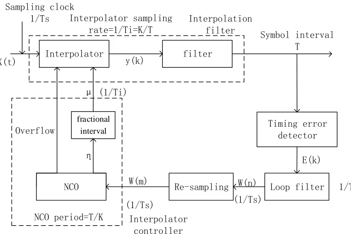
At present, the extraction of timing error is mainly based on the Gardner timing synchronization loop and Farrow interpolation [8]. The loop is mainly composed of interpolation filter, timing error detector (TED), and loop filter and interpolation controller. The block diagram is shown in Figure 1. Wherein the interpolation filter is used to generate the interpolation result, which is essentially the secondary extraction of the interpolation result that is filtered by low-pass filter. The timing error detector can estimate the timing error which is proportional to the true timing error according to the interpolation filter output, the error resamples after filtering its high frequency components and clutter by passing the loop filter, and the result of it will feedback to the interpolation controller to calculate the new basepoint index and fractional interval ,which are finally sent to the interpolation filter to be used as the parameters in next turn of interpolation .This above process constitute a feedback loop, which run iteratively until the output of timing error detector is 0 or a constant.
Interpolator filter
Timing error detector
fractional interval
Re-sampling Loop filter NCO
Sampling clock 1/Ts
X(t) y(k)
μ
η Overflow
NCO period=T/K
W(m)
(1/Ts)
W(n) (1/Ts)
E(k)
1/T Symbol interval
T Interpolator sampling
rate=1/Ti=K/T
(1/Ti)
Interpolator controller
[image:2.612.116.476.361.601.2]Interpolation filter
Figure 1. The diagram of Gardner timing synchronization loop.
The interpolation equation of the Gardner interpolation filter is:
2
1
( ) (( ) ) [ ( ) ][ ( ) ]
I
i k k s k s k s
I
Where mk is the basepoint index, k is the fractional interval of the interpolation,
1
I and I2 is the order of interpolation filter. In the timing synchronization process, the interpolation filter calculates the interpolation result by using basepoint index and fractional interval. The error function of timing error detector can be expressed as Equation 2:
1 1
( ) ( )[ ( ) ( 1)] ( )[ ( ) ( 1)]
2 2
I I I Q Q Q
E k y k y k y k y k y k y k (2)
Where y k( ), ( 1) 2
y k , y k( 1) represent the interpolated results with the interval of
/ 2
s
T respectively. The traditional interpolation controller is a phase-decremented NCO structure, its difference equation is:
(m 1) [ ( )m W m( )]mod 1
(3)
Where ( )m the phase-controlled word of NCO is, W m( ) is the increment of NCO phase decremented which is output and controlled by the loop filter.
Since the value of k can be selected arbitrarily in the range of 0 to 1, so the filter
weighting factor h i( ) in formula 1 must be calculated in real time according to the value of k, which is not conducive for hardware implementation. At the same time,
for the ultra-high-speed receiver, when the symbol rate of signal is greater than 1.2Gsps and the sampling rate of front-end ADC approaching 4.8Gsps, the traditional serial implementation method is basically not applicable, the use of parallel digital structure also need at least 8 parallel multi-phase filters, which is pretty costly for the whole system and is difficult for digital chips to bear.
ULTRA-HIGH-SPEED PARALLEL BIT SYNCHRONIZATION ALGORITHM
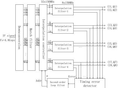
Interpolation filter-1 Interpolation filter-2 Interpolation filter-3 Interpolation filter-4 Second-order loop filter ... ... I1 I2 I3 I32 Q1 Q2 Q3 Q32 ... I1 I2 I3 Q1 Q2 Q3 Q32 I32 ... 1 2 8 ... 10 16 ... 18 24 ... 26 32 9 17 25 Timing error detector ... (I1,Q1) (I2,Q2) (I3,Q3) (I4,Q4) (I5,Q5) (I6,Q6) (I7,Q7) (I8,Q8) ... Error μ Addr IF signal Fs=4.8Gsps 32x150MHz 8x150MHz Downconversion Match filter Interpolation controller
Figure 2. The FPGA implementation diagram of ultra-high-speed parallel timing synchronization.
Assuming that the clock of FPGA is Fc, the sampling rate of system is Fs, and
then we can get the number of symbols which need to be recovered for each system clock is H Fs/Fc. Each timing error detector actually outputs two best sampling points, so we need N H / 2 error calculation channels and parallel interpolation channels. By Equation 2 we can see that the calculation of each timing error requires three adjacent interpolation results, so each error detection channel requires three four-point interpolators.
The traditional interpolation methods include cubic interpolation [9], segmented parabolic interpolation and linear interpolation etc. Among which cubic interpolation has better performance and is fit for hardware implementation. In this paper, we choose cubic interpolation and use the quadratic, four-order Farrow structures to approximate the interpolation filter polynomial shown in Equation 1, as shown in Equation 4:
1
2
( i) i (( k ) )s
i
y kT c x m i T
(4)Where the value of ci is satisfied:
3 3 2 3 2 3 2
2 1 0 1
1 1 1 1 1 1 1 1 1
, , 1,
6 6 2 2 2 2 6 2 3
c c c c (5)
where the value of n is 10, normalize and store the four groups of ci into block ROM
in FPGA, afterwards we get the lookup table, with which we can update the coefficients in real time. According to the principle of bit synchronization interpolation controller, assuming that the fractional interval does not change, we can get the initial value of the basepoint index as follows:
,1 8*( 1) 1; ,2 8*( 1) 3; ,3 8*( 1) 5;
N N N
m N m N m N (6) We use fractional interval and basepoint index to control the calculation in interpolation filter. The four points for interpolation are cached, we denote it as
InterVector, the deep of the data cache is H+2*P, and the interpolation coefficients
of the four channels are fetched from the lookup table according to the address in the Equation 7, we denote it asCoeVector. The interpolation calculation is shown as Equation 8:
_ ( / 2m n) ( 1, 2,3, 4)
addr x floor x (7)
, ( , : , 3)
i j i j i j
InterOut InterVector m m CoeVector (8)
And the N channel timing error detection results can be indicated as:
,2 ,1 ,3 ,2 ,1 ,3
Re[ ] Re[ ] Im[ ] Im[ ]
i i i i i i i
TEDOut InterOut InterOut InterOut InterOut InterOut InterOut
(9) The average value of the loop filter output can be obtained by making the interpolation results through the loop filter, we use the conventional two-order digital phase-locked loop[10] in this design, the output can be expressed as:
1 2
( ) ( N) /
W m LPOut LPOut LPOut N (10)
In order to facilitate the implementation in FPGA, we transfer the NCO structure in Equation 3 into phase-incremental structure, the difference equation is:
(m 1) ( )m W m( )
(11) Finally, we update the decimal interval and basepoint index in the interpolation controller according to the output of the NCO. This feedback loop will remain iterative until the output of timing error detector is a constant. It should be emphasized that this algorithm eliminates the updating process of basepoint index by designing the state machine in a rational way.
achieves the continuous updating of the interpolation input and the fractional interval by controlling the operation of state machine and finally outputs the timing synchronization result with great performance.
PERFORMANCE SIMULATION
The algorithm is suitable for any "amplitude-phase" joint modulation constellation and can greatly improve the data throughput of timing synchronization with less hardware cost. In this case, we set QPSK system as an example and use Xilinx XC7VX485T series FPGA chip and 4.8Gsps ADC as the development platform. In this system, FPGA operating clock is 150MHz, symbol rate Rs=1.2Gsps. We can get
the oversampling rate is PFs/R s4, the number of parallel timing error detection
channel is N Fs /Fc/ 2 16 and the four-point interpolation block diagram shown in Figure 3.
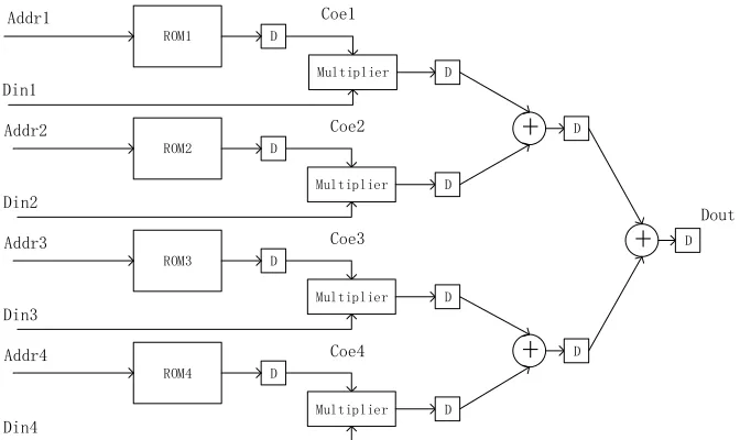
This algorithm does not need to update the interpolation basepoint index, so we only need to set its initial value. In order to ensure the accuracy of the fractional interval, we quantify the value of it into 32 bits, and use its top 10 bits as the index of the lookup table so that we can update interpolation coefficients in real time. The update of interpolation input data and fractional interval is controlled by state machine, we can describe its rules of operation as Figure 4.
ROM1 D
Addr1 Coe1
Multiplier
Din1
D
ROM2 D
Addr2 Coe2
Multiplier
Din2
D
ROM3 D
Addr3 Coe3
Multiplier
Din3
D
ROM4 D
Addr4 Coe4
Multiplier
Din4
D
+
+
D
D
+
D [image:6.612.133.469.365.565.2]Dout
1
9
8
7
6
5
4
3
2
0
a
b
c
c
b
a
c
a
b
b
c
a
b
c
a
b
c
a
b
c a
b
c
a
b
c
a
b
c
a
[image:7.612.190.408.58.242.2]a: η≥1 b: η<0 c: 1>η≥ 0
Figure 4. Operation of interpolation-controlled state machine.
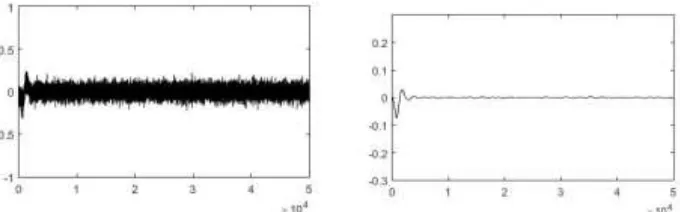
[image:7.612.131.452.390.515.2]Follow the processes above and then we can get the current synchronization results. We finally achieve the timing synchronization of QPSK system whose symbol rate is 1.2Gsps and the sampling rate is 4.8Gsps. Figure 5 and Figure 6 give the constellation and output of timing error detector as well as its filtered result in the condition of the signal-to-noise ratio of 20dB, we can see that when the loop tends to be stable, the timing error has very little jitter and eventually convergent to zero.
Figure 5. Constellation before timing synchronization (left) and after timing synchronization (right).
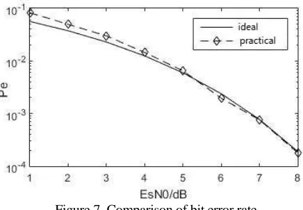
[image:7.612.128.468.568.674.2]Figure 7. Comparison of bit error rate.
We take 7,000,000 symbols and set SNR = 1: 1: 8 to draw the bit error rate curve of our synchronization system and the ideal QPSK system, we can see that the practical curve almost coincides with the ideal one, so we can draw the conclusion that our design has an ideal performance in terms of bit error rate.
SUMMARY
In the paper, we propose an ultra-high-speed all-digital parallel timing synchronization algorithm based on FPGA, which is suitable for any "amplitude-phase" joint modulation constellation. The algorithm uses the lookup table structure to realize the real-time update of the interpolation filter coefficient more efficiently. Meanwhile the reasonable design of state machine also eliminates the updating process of the interpolation basepoint index, which can be widely applied to other parallel interpolation structures. In addition, the algorithm breaks through the limitation of the sampling rate in digital device which used to be a critical problem encountered by traditional serial bit synchronous structure. This design can greatly increase the throughput of data without paying too much hardware cost in the case of low clock frequency. We finally achieve the implementation of QPSK system with 1.2Gsps symbol rate and 4.8Gsps sampling rate on FPGA, however, this algorithm can be expanded to higher speed use and has broad application prospects.
REFERENCES
1. Du Yong. Implementation of synchronization technology in digital communication Based on Matlab and FPGA. Publishing house of Electronics Industry, 2015, p.2-4.
2. Xue Chen. A Doppler Compensation Algorithm in the Wireless Mobile Communication System Based on FPGA. Modern radar. Vol. 37 (2015) No. 7, p. 30-33.
3. Ling Yu: Ultra - high - speed real - time communication system based on software radio technology (Master's degree, XiDian University, China, 2015).p.39-43.
4. Liu Siyuan, Chen Jianjun, Zhang Xin. Design and Matlab simulation of an all-digital QPSK demodulator. Journal of Nanjing University of Information Science. Vol. 6(2014) No.3, p.226-230. 5. Gardner F.M. Interpolation in digital modems-Part I: Fundamentals. IEEE Transactions on
Communications. Vol. 41(1993), p. 501–507.
7. Hu Mingrui, Chen Changxing, Feng Xiaoyu. Investigation on the Bit Synchronization Algorithm Simulation of the Satellite Launching and Receiving Signal. Computer Simulation. Vol. 33(2016) No.9, p.127-131.
8. Song Qingping, Liu Rongke, Duan Ruifeng. A symbol timing synchronization algorithm for all digital receiver. Journal of Terahertz Science and Electronic Information Technology. Vol. 13(2015) No.3, p.436-440.
9. Wang Yuping: Design and Implementation of QPSK Modulation and Demodulation Based on FPGA (Master's degree, Chengdu University of Technology, China, 2015). p. 29-34.