HARDWARE EMULATION OF A SECURE PASSIVE RFID SENSOR SYSTEM
A Thesis Presented
by
MICHAEL TODD
Submitted to the Graduate School of the
University of Massachusetts Amherst in partial
fulfillment of the requirements for the degree of
MASTER OF SCIENCE IN ELECTRICAL AND COMPUTER ENGINEERING
September 2010
© Copyright by Michael Todd 2010
HARDWARE EMULATION OF A SECURE PASSIVE RFID SENSOR SYSTEM
A Thesis Presented
by
MICHAEL TODD
Approved as to style and content by:
________________________________________
Wayne P. Burleson, Chair
________________________________________
Sandip Kundu, Member
________________________________________
Russell Tessier, Member
_______________________________________
C.V. Hollot, Department Head
DEDICATION
v
ACKNOWLEDGEMENTS
First and foremost, I would like to thank Wayne Burleson for providing me with
the opportunity to expand my knowledge of electrical and computer engineering, and for
his guidance and support throughout my research. I would also like to thank Professor
Christof Paar for guidance in the state-of-the-art of security engineering. Thanks should
also be given to Professor Kevin Fu and his team in the Computer Science department
here at UMass for their pioneering work in advanced RFID related topics. I would like to
thank Professor Wayne Burleson, Sandip Kundu, and Russell Tessier for their service on
my thesis committee. I would also like to thank the entire VLSI Circuits and Systems
group for both their friendship and academic support, specifically Serge Zhilyaev, Basab
Datta, and Ibis Benito.
A great many thanks should also be given to my family Mark, Lori, Nathan,
Jason, and Benjamin for their encouragement and support throughout my life and
academic career and without whom none of this would be possible. Finally, I would like
to thank my beautiful bride-to-be Amanda Burk. She has been there through every step of
vi
ABSTRACT
HARDWARE EMULATION OF A SECURE PASSIVE RFID SENSOR SYSTEM
SEPTEMBER 2010
MICHAEL TODD, B.S., UNIVERSITY OF MASSACHUSETTS AMHERST
M.S.E.C.E., UNIVERSITY OF MASSACHUSETTS AMHERST
Directed by: Wayne Burleson
Passively powered radio frequency (RFID) tags are a class of devices powered via
harvested ultra high frequency (UHF) radiation emitted by a reader device. Currently,
these devices are relegated to little more than a form of wireless barcode, but could be
used in a myriad of applications from simple product identification to more complex
applications such as environmental sensing. Because these devices are intended for large
scale deployment and due to the limited power that can be harvested from RF energy,
hardware and cost constraints are extremely tight.
The Electronic Product Code (EPC) Global Class 1 Generation 2 (Gen2)
specification [EPC08] is currently the de facto communication standard for passively
powered RFID. One issue restricting deployment and a cause for some privacy concerns
is a lack of security in the Gen2 protocol. We will demonstrate a potential solution to this
problem by using a novel block cipher designed for low power and area constrained
devices to encrypt and transmit sensor data. This will be done while maintaining
backward compatibility with the original standard and will require no substantial changes
to the reader. Our solution will also provide one way authentication, data integrity
vii
In this thesis we will demonstrate an FPGA emulation of a Gen2 compatible
RFID tag which will serve as a test bed for several novel features. We will leverage prior
work involving several aspects of a tag [QL09] [PP07] as well as incorporate a novel low
power encryption cipher [AB07] and external temperature sensor. Demonstrated in
[CT08], FPGA emulation will allow for the independent verification of several
components. This thesis will provide insight into the future of RFID and will provide
viii
TABLE OF CONTENTS
Page
ACKNOWLEDGEMENTS………
ABSTRACT………...
LIST OF FIGURES...
LIST OF TABLES………..
LIST OF ALGORITHMS...
CHAPTER
1. INTRODUCTION TO RFID………..
1.1 Motivations...
1.2 EPC Class-1 Generation-2 RFID Standard………..
1.3 Prior Work...
1.3.1 WISP……….
1.3.2 FPGA RFID Sensing Platform………..
1.4 Thesis Outline………..
2. DESIGNING A GEN2 TAG……….……….
2.1 Design Methodology……….…………
2.2 Gen2 Basics………..
2.3 Typical Tag Inventory Session……….
2.4 Gen2 Tag Hardware………..
2.5 Basic Digital Backend……….
2.6 PIE Decoder………
2.7 CRC5 & CRC16……….…….
2.8 Backscatter Encoding………..
2.8.1 FM0 Encoding……….……….
2.8.2 Miller Encoding………
2.9 Memory………...
3. SECURE SENSING WITH A GEN2 TAG………..
3.1 Environmental Sensing with a Gen2 Tag………
v
vi
xi
xiii
ix
1
1
2
3
3
4
5
6
6
7
8
9
10
11
12
13
14
15
16
18
18
ix
3.2 Security Motivations...
3.3 Security in Gen2……….………….
3.4 Securing Sensor Data………..
3.4.1 Guidelines………
3.4.2 Adversary……….
3.4.3 Security Protocol………..
3.5 Security Analysis………
3.5.1 Security Basis………..
3.5.2 CV
40……….………
3.5.3 TRN
80………..
3.6 Security Protocol Proof of Concept………
4. ENHANCING THE DIGITAL BACKEND……….………
4.1 Enhancement Overview………..
4.2 PRESENT………
4.2.1 PRESENT Algorithm………...
4.2.2 PRESENT Key Scheduler………
4.3 LAMED………...
4.4 Dual Clocking Scheme………
4.5 Temperature Sensor….………
5. DESIGN EMULATION & VALIDATION………..
5.1 Our Platform………
5.2 Validation………
5.2.1 Validation Overview………
5.2.2 RFID Reader………
5.2.3 Validation Milestones….……….
5.3 Supported Gen2 Structure………...
5.4 PRESENT Validation & Decryption……….……….
5.5 Synthesis Results & Discussion………..
5.6 Video Demonstration………..
6. CONCLUSIONS………...
6.1 Timeline………..
6.2 Our Contributions………
19
20
22
22
23
23
26
26
27
28
29
31
31
32
32
34
34
36
37
39
39
41
41
42
42
44
45
46
48
49
49
49
x
6.3 Future Work………
APPENDICES
A.
PRESENT ENCRYPTION VERILOG……….
B.
LAMED PRNG VERILOG………..
C.
CRC16 VERILOG………
D.
CRC5 VERILOG………..
E.
BACKSCATTER CLOCK DIVIDER VERILOG………
F.
PIE DECODER VERILOG………..
G.
TPRI VERILOG………
H.
DATA TRANSMISSION VERILOG………..
I.
PRIMARY FSM VERILOG……….
J.
DS1620 TEMPERATURE SENSOR VERILOG………...
K.
MEMORY BANKS VERILOG………..
L.
PRESENT DECRYPTION VERILOG………...
M.
WAVEFORM TEXT FILE TO VERILOG TESTBENCH SCRIPT…………..
REFERENCES………
50
52
56
60
61
62
66
73
76
87
125
128
131
135
138
xi
LIST OF FIGURES
Figure
Page
1. From [TF06], [WI10], [DD08] Passive vs. Active RFID………
2. Wireless Sensing Platform………..
3. From [CT08], FPGA emulation of Gen2 compliant RFID sensing platform………….
4. Basic RFID system diagram adapted from [DD08]………
5. Typical tag inventory session………..
6. The two primary components of a traditional passive RFID tag….………..
7. Block diagram depiction of the digital backend of Gen2 RFID tag………..
8. From [EPC08] PIE encoding……….
9. Schematic depiction of reader-to-tag data link adapted from [DD08]………..
10. From [EPC08] the RTcal symbol………
11. PIE Decoder state diagram……….….
12. From [EPC08] Schematic view of the a) 5 bit CRC and b) 16 bit CRC……….
13. Transmission encoder circuit………..
14. From [EPC08] FM0 encoding sequences………
15. From [EPC08] subset of Miller encoding sequences………..
16. Memory configuration………
17. RFID tag with sensor block diagram adapted from [FT09], [IPJ08]………..
18. RFID sensor application illustration………
19. From [AM07] standard vs. secure command flow………..
20. Security scheme proposed in [DB06]……….
21. Online portion of secure data transfer……….
1
3
4
7
9
10
10
11
11
12
12
13
15
15
16
17
18
19
20
21
24
xii
22. Offline tag data upload and integrity check………..………..
23. Block cipher counter mode……….
24. Sensor data security scheme POC command flow……….
25. Block diagram depiction of our enhanced Gen2 digital backend………
26. From [AB07] a gate equivalence comparison of optimized block ciphers………….
27. From [AB07] PRESENT algorithm block diagram………
28. From [QL09] PIE sampling error………
29. Simulated output of the temperature sensor FSM………...
30. FPGA RFID sensing platform block diagram………
31. Photograph of our FPGA RFID sensing platform………..
32. Circuitry required to integrate the FPGA with the WISP and sensor……….
33. Illustration of I/O capture to verilog testbench………...
34. RFID reader software interface used in design validation………..
35. Supported Gen2 FSM structure………..
36. Gate equivalence synthesis results of our design………
37. Thesis verilog lines of code breakdown………..
25
26
30
31
32
33
37
38
39
40
40
43
44
45
46
47
xiii
LIST OF TABLES
Table
Page
1. From [GEN2] set of commands required by a Gen2 compliant RFID tag……….……
2. Bit length for the subset of reader commands required in our security protocol…….
3. Bit length for data transmitted by the tag in our security protocol………..
4. Data transfer timing calculation summary………
5. From [AB07] PRESENT sbox layer substitution mapping………..
6. From [AB07] PRESENT permutation layer……….
7. Range of Gen2 parameters verified………..
8. Validation milestones………
9. Thesis project timeline………..
8
27
27
28
33
34
42
44
49
xiv
LIST OF ALGORITHMS
Algorithm
Page
1. PRESENT key scheduling algorithm………
2. LAMED PRNG Algorithm………
34
1
CHAPTER 1
INTRODUCTION TO RFID
1.1 Motivations
Passive RFID tags are essentially a low cost integrated circuit (IC) and antenna
that harvest RF energy and use it to power a small amount of analog circuitry, digital
logic, and non-volatile memory. Passive tags do not have a battery and thus lack a way to
actively transmit data. Instead, a process known as
backscatter
is used to reflect RF
energy transmitted to the tag back to the reader. Fig. 1a from [DD08] illustrates the
difference between an active and a passive RFID tag. An example of each is given in Fig.
1b, showing that active tags are much larger and are used in applications such as
automatic toll collection. Passive tags are significantly smaller and are typically used in
inventory tracking applications [TF06], [WI10].
Figure 1: From [TF06], [WI10], [DD08] Passive vs. Active RFID. a) Passively powered RFID tags lack an independent power supply and must derive power and data from RF energy emitted by a reader, and communicate by reflecting RF energy back to the reader. b) Passive tags are significantly smaller and lower cost than active tags and could possibly be used in a greater number of applications.
2
Passive tags are primarily intended to function as a form of “wireless barcode”
used for tracking, inventorying, and even preventing theft of merchandise. Arguably, the
most high profile deployment of RFID technology was a mandate in 2004 when
Wal-Mart told its 100 top suppliers to provide RFID tags on all cases and pallets delivered to
Wal-Mart by January 2005, with the next 100 to follow a year later [DD08]. Such high
volume deployment inherently forces tight area constraints on these devices to reduce
cost. Most claim these devices are generally in the range of 5k gates with a target price of
1-5¢ [PP09].
1.2 EPC Class-1 Generation-2 RFID Standard
The EPCglobal Class-1 Generation-2 Radio-Frequency Identity Protocol for
Communications at 860 MHz – 960MHz, which we will refer to as Gen2 throughout the
remainder of this work, “defines the physical and logical requirements for a
passive-backscatter, Interrogator-talk-first (ITF), radio-frequency identification (RFID) system”
[EPC08]. This standard has been widely accepted as the primary standard for passively
powered RFID tags since its inception by EPCglobal in 2004 and the International
Organization for Standardization (ISO) 18000-6C in 2006.
There have been several published works involving designs which incorporate
Gen2 directly [AM07], [CT08], [AM07] or seek to improve upon specific portions of the
protocol [DB06], [QL09], [PP07], [AN07]. It is our goal to incorporate and build upon
many of these works and create a type of guide to implementing Gen2 compliant tags.
We
do not
however make the claim that our implementation is either 100% Gen2
3
were able to design, validate, and emulate a design capable of communicating with a
Gen2 compliant RFID reader.
1.3 Prior Work
1.3.1 WISP
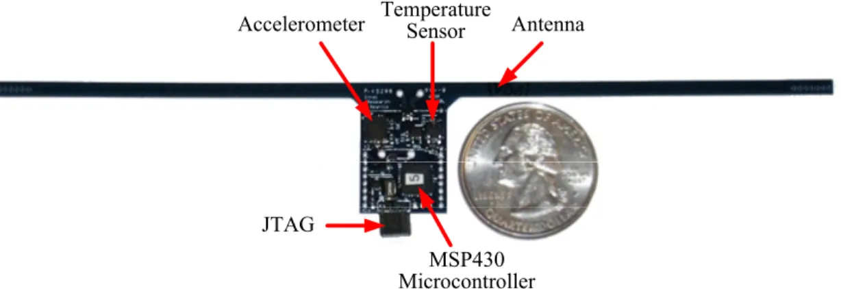
The Wireless Sensing Platform (WISP) is a prototype RFID tag shown in Fig. 2.
The WISP was designed by Intel and is a partially Gen2 compliant RFID tag constructed
from a low power MSP430 microcontroller, analog circuitry, temperature sensor, and
accelerometer [SA08]. It is in essence a software programmable RFID tag and has been
utilized in several publications [HC07], [DH08], [SC09].
Figure 2: Wireless Sensing Platform. WISP is designed from a low power MSP430 microcontroller, and includes several onboard sensors.
The WISP has been proven successful in many applications including medical
devices [DH08], recognizing human activities [MB09], and light sensing [RS06], though
the relatively large size and high cost would make such a device impractical for high
volume deployment. Also, modularizing the software required to both perform the Gen2
protocol, and any additional computation in the face of intermittent power from harvested
RF energy provides a significant challenge. Our work will build upon the work pioneered
by the WISP in two ways. First, we will leverage the idea of directly incorporating
Accelerometer Temperature Sensor AntennaJTAG
MSP430 Microcontroller
4
additional functionality into a Gen2 RFID tag with our block cipher and external sensor.
This will provide a low cost solution to a Gen2 compliant, environmental sensing, and
secure RFID tag. Second we will prototype our device on an FPGA. This will create a
sister device to the WISP, a hardware programmable RFID tag.
1.3.2 FPGA RFID Sensing Platform
The idea of a hardware programmable, Gen2 compliant RFID sensing platform
was first demonstrated in [CT08] and is shown in Fig. 3. FPGA emulation provides two
major advantages over simulation. The first is proof of compliance with Gen2, as we will
be using an RFID reader known to be compliant, discussed further in section 5.2. The
second is a reduction in simulation time. Communication in Gen2 occurs on the order of
milliseconds, which can lead to long simulation time as we integrate a greater number of
modules in our design. We will replicate and build upon the work presented in [CT08] by
introducing a way to secure the sensor data.
5
1.4 Thesis Outline
In this thesis we will begin with an overview of the Gen2 protocol followed by a
block by block breakdown of each portion of the design. Chapter 3, justifies using a Gen2
RFID tag for environmental sensing and the security implications. Chapter 4 discusses
the enhancements required to implement our approach to security. Finally, we will
explore the validation and emulation aspects of our work including how we were able
6
CHAPTER 2
DESIGNING A GEN2 TAG
2.1 Design Methodology
Both the design and validation portions of our project were done in the Verilog
Hardware Definition Language (HDL) with compilation and simulation being done in the
Xilinx ISE 9.2.04i environment. As previously mentioned, in a commercially viable
RFID tag gate count and power consumption are of primary concern. The focus of our
project is ease of reuse in the HDL code. This will allow our work to serve as a testbench
for changes and optimizations to Gen2 and security protocols, as well as reducing both
ramp-up and debug time. To accomplish this goal, implementation was guided by several
important design rules:
1.
Make the design highly modularized, rather than integrated.
2.
Thoroughly commented code with external references where appropriate.
3.
The manner by which each module is enabled, reset, and completion is
indicated should remain standard.
It is our desire that by utilizing said guidelines we will be able to greatly reduce
the complexity of the design at the cost of size and allow components of the design to be
replaced with ease. With that being said we have made a reasonable effort to reduce the
size of our design. Discussed further in section 5.5, we have synthesized our design and
7
2.2 Gen2 Basics
In this protocol the interrogator (reader) modulates a signal in the UHF frequency
range (860-960MHz) in order to communicate with a receiver (tag). The tag uses this
signal not only to receive data, but to power the device via RF energy harvesting. The
reader receives data from a tag by transmitting a continuous wave while the tag
modulates the reflection coefficient of its antenna in a process known as backscatter. This
can be thought of as basically creating an open circuit or short circuit across the antenna
to generate a 0 or 1. Fig. 4 is an illustration of a basic RFID system.
Figure 4: Basic RFID system diagram adapted from [DD08]. A computer sends commands through the reader device to the tag. The tag then responds with stored information accordingly.
The reader controls several aspects of each communication session such as both
downlink (R
T) data rate between 50-215 kbps, and uplink (T
R) data rate between
5-640 kbps. The reader also controls what information the tag backscatters. Tags must
support a basic set of commands given in Table 1. Tags are also assumed to have some
form of non-volatile memory such as flash, where they store the Electronic Product Code,
denoted as EPCID throughout this work, which can be thought of as the ID of the tag, as
8
Table 1: From [GEN2] set of commands required by a Gen2 compliant RFID tag. There are also several non-mandatory commands, as well as opcodes reserved for custom commands to allow for flexibility.
Command Opcode QueryRep 00 ACK 01 Query 1000 QueryAdjust 1001 Select 1010 NAK 11000000 Req_RN 11000001 Read 11000010 Write 11000011 Kill 11000100 Lock 11000101
2.3 Typical Tag Inventory Session
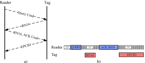
Fig. 5 depicts a typical reader-tag inventory session, both data flow and in time.
RN16 is a 16 bit pseudo random number generated by the tag used in access control and
to confirm that the reader intended to speak to this tag when the reader transmits RN16
back to the tag. EPCID is the ID of the individual tag. This sort of inventorying session is
an example of a passive tag used as little more than a wireless barcode. It should also be
noted that CW stands for continuous wave, which is the unmodulated 900MHz RF
energy emanated by the reader to power the tag during computation and is reflected
9
Figure 5: Typical tag inventory session. a) Data flow representation. b) In time representation.
2.4 Gen2 Tag Hardware
Fig. 6 illustrates the basic building blocks of a Gen2 RFID tag. The two primary
modules of the tag are the analog frontend and digital backend. The frontend is
responsible for regulating the incoming RF signal to generate V
DDfor the digital logic,
generating a clock signal, and demodulating the incoming data. The frontend also
contains the backscatter transistor used to alter the reflection coefficient of the antenna
during T
R communication. Though this work will fully concentrate on the portion
labeled Digital Components & Control Logic, a cursory understanding of the remainder
10
Figure 6: The two primary components of a traditional passive RFID tag. Our work will concentrate on the design and modification of the digital components and control logic.
2.5 Basic Digital Backend
Fig 7. is an expanded view of the components that make up the basic digital
backend of a Gen2 RFID tag. The basic blocks consist of the incoming data decoder, the
backscatter clock generator, output data encoder, cyclic redundancy checkers (CRC5/16),
pseudo random number generator (PRNG), memory controller, and command handler
finite state machine. Next we will delve into the implementation details for several of
these components.
Figure 7: Block diagram depiction of the digital backend of Gen2 RFID tag.
FM0/Miller
Encoder
PRNG
16 16 5Command
Handler
FSM
RN16CRC5
CRC16
Memory
Banks
16PIE
Decoder
demod_data_in data_outBackscatter
Clock Divider
blf_clk (40-640kHz)11
2.6 PIE Decoder
Pulse interval encoding (PIE) is the encoding scheme used for R
T
transmissions. Fig. 8 demonstrates how binary symbols are represented in this encoding
scheme.
Figure 8: From [EPC08] PIE encoding. Encoding is achieved by varying the amount of time each symbol is high.
The reason for using this encoding scheme can be explained through
understanding Fig. 9 from [DD08]. Here we can see that to simplify the decoder,
amplitude modulation (AM) is used. Recalling that the tag also harvests power from this
signal, whenever the amplitude of the incoming RF signal is low, the tag is not receiving
power. Therefore, we must use an encoding scheme in which the incoming RF signal is
high for the majority of the time. Though in Fig. 9 the low in the 0 and 1 seems to be a
significant portion of the symbol, in reality this will be a much smaller fraction.
Figure 9: Schematic depiction of reader-to-tag data link adapted from [DD08].
In order to decode the data, we sample the incoming demodulated data when the
data is high. Fig. 10 illustrates the R
T calibration symbol (RTcal) which is transmitted
0
1
Amplitude modulation Modulation depth 90% Pulse-interval encoding (PIE)Reader
Tag
Data12
at the beginning of each reader command. We sample RTcal and divide this number by
two resulting in the pivot. For the duration of the current command we interpret any
symbol shorter (less samples) than the pivot to be a 0 and any symbol larger to be a 1. A
detailed description of the PIE decoder state machine is given in Fig 11.
Figure 10: From [EPC08] the RTcal symbol. Symbol is transmitted at the beginning of each reader command and is used to calibrate the R-->T data link.
Figure 11: PIE Decoder state diagram. The concept is to sample RTcal and divide by 2 to calculate the pivot. Each subsequent symbol shorter than the pivot is interpreted as a 0 any longer are interpreted as a 1.
13
Our decoder utilizes an array containing all supported opcodes, and the bit length
of each command. After receiving a symbol, we compare with the array, and upon
finding a match, raise the opcode_ready flag. This allows the command handler FSM
time to perform certain tasks in parallel with the command decoding such as pseudo
random number generation or retrieving values from memory. We then use the same
array to indicate we have received all of the data associated with the command and raise
the data_ready flag.
2.7 CRC5 & CRC16
Included in the Gen2 are 5-bit and 16-bit cyclic redundancy checks, called CRC5
and CRC16 respectively. Both of these circuits are constructed from a linear feedback
shift register (LFSR) and are used to safe guard information against bit errors during
transmission. Schematics for both circuits are given in Fig. 12 from [EPC08].
14
CRC5 is only utilized when confirming a Query command was properly received.
For this reason we were able to modularize the control logic. We used a 22 bit shift
register which resets the CRC5 if a Query opcode is received and loads the contents of
the Query command when the PIE decoder data_ready flag is raised and begins to shift in
the data. If the Query command is properly received based on Appendix F of [EPC08],
the crc5_valid flag is raised.
The CRC16 is used both to confirm certain commands were properly received,
and to protect transmitted data, making implementation slightly more challenging, but the
basic operating principles remain the same as the CRC5. We use a larger shift register
and each time the CRC16 is used, data is loaded into crc16_data_in, crc16_reset is raised,
and the number of bits to be clocked into the CRC16 is loaded into crc16_count. We then
shift crc16_data_in by one position and decrement crc16_count until we reach 0.
Depending on whether we are computing or verifying a CRC16 value we will either raise
the crc16_valid flag or compare to a fixed value according to Appendix F of [EPC08] and
raise the crc16_valid flag.
2.8 Backscatter Encoding
Gen2 requires that the tag support two data encoding schemes for T
R
communication, FM0 and Miller. In keeping with design modularity, we designed a
transmission circuit (tx_fsm) shown in Fig. 13, charged with selecting the correct
encoding scheme and transmitting the appropriate preamble and data. Inputs to tx_fsm
are the number of bits to be transmitted, a 2 bit m value for selecting the encoder, and
trext for selecting the preamble length. A 129-1 multiplexer selects the appropriate bit to
15
blf_clk and data is clocked into the encoders on the following positive blf_clk edge.
When all bits have been transmitted the tx_complete flag is raised.
Figure 13: Transmission encoder circuit. The input register is preloaded with the data being transmitted to the reader. A counter is used to select the appropriate bits. The m value selects the appropriate encoding scheme. When the counter reaches the number of bits the tx_complete flag is raised. Trext is used to indicate the length of the preamble.
2.8.1 FM0 Encoding
Fig. 14 from [EPC08] is a waveform of all possible FM0 sequences. The output is
toggled at the start of each symbol. FM0 encoding requires a phase change on the
negative edge of the blf_clock when transmitting a 1 and no phase change when
transmitting a 0. Therefore, the data rate in FM0 encoding is equal to the backscatter link
frequency.
16
2.8.2 Miller Encoding
Miller encoding works in a manner similar to FM0. The difference between a 0
and 1 is based on 180º phase shift, but with a more complex set of guidelines. To begin
with, there is what is known as a subcarrier value (m) that determines the number of
clock cycles required to transmit a single bit of data. Therefore, the data rate is the
backscatter link frequency/m. A tag is required to support m values of 2, 4, & 8. Fig. 15
is a representative set of Miller encoded sequences. Also shown in Fig. 15 are the rules
for when it is appropriate to change phase. This occurs on the boundary between
consecutive 0’s and on the m
thclock edge of every data 1 symbol.
Figure 15: From [EPC08] subset of Miller encoding sequences.
2.9 Memory
As mentioned in section 1.1, Gen2 tags must contain some form of non-volatile
memory used to store information such as the EPCID and access passwords. Section
6.3.2 of [EPC08] states this memory must be partitioned into 4 banks User, TID, EPC,
and Reserved. Data is accessed in 16 bit words. For simplicity we chose to simulate
memory with a set of 2-dimentional register arrays, addressed by the 2 bit mem_bank
value, and the mem_word byte. We use a bit called write_enable to distinguish between
17
Figure 16: Memory configuration. For our prototype we chose to emulate non-volatile memory with a set of four 2-dementional arrays.
Because the register array is not actually non-volatile we also included a
mem_reset input which resets the register arrays to a specific state. The act of resetting
the memory also serves to hard code information such as the EPCID. It should be noted
that we did not include any form of access control to prevent reads or writes to and from
specific memory locations, though such a scheme would be a straightforward extension
to the current architecture.
USER BANK EPC BANK TID BANK RES BANK 8 16 16 16 16 16 Row Select mem_word 2 mem_bank mem_in 16 16 16 16 mem_out
18
CHAPTER 3
SECURE SENSING WITH A GEN2 TAG
3.1 Environmental Sensing with a Gen2 Tag
The combination of a moderate read range of 10-30 ft [DD08], non-volatile
memory, low cost reader hardware, and power harvesting make Gen2 tags well suited to
function as the communication frontend for a sensor. This idea is evident in the design of
the WISP which includes a temperature sensor and accelerometer and could be used for a
variety of applications [HC07], [DH08], [SC09]. The basic principle being that in the best
case, the power harvested by the tag could be used to power the sensor. While at the very
least, the tag could serve as the communication frontend for the sensor, eliminating the
power required to transmit data and allowing the sensor to last longer if it has a battery or
harvest less energy from another source such as solar.
Figure 17: RFID tag with sensor block diagram adapted from [FT09], [IPJ08]. Power for the sensor could ideally come from the tag's harvesting circuitry, but could also be from a separate source such as a battery or solar. With no power drawn from the sensor to transmit the data battery life of the sensor would be extended or the sensor would function in less ideal conditions.
In [CT08] temperature sensor data was incorporated into the EPCID value and
transmitted over an unsecured channel. We would like to take this a step further and
provide a level of security by incorporating a novel low power block cipher. In this
19
3.2 Security Motivations
Fig. 18 illustrates an example application in which we would want to protect
sensor data. We will reference this application throughout this chapter. In this example,
the bridge has been embedded with several sensors with RFID frontends. If we assume
that our bridge is located in a remote location, constant monitoring of the tag could be
considered challenging and expensive. Instead, periodically a vehicle equipped with an
RFID reader passes over the bridge and collects the sensor data. The vehicle then returns
to a secure location and downloads the information for later processing.
Figure 18: RFID sensor application illustration. Here we depict a vehicle periodically driving over the bridge to retrieve sensor data. This could simplify the infrastructure required to monitor the bridge, though several security implications must be considered.
This scenario could justify several layers of security. We would not want to reveal
the sensor data to an untrusted reader because this might allow a malicious party to
discover and target a weak point in the bridge if it were a mechanical stress sensor. We
would also like to obscure the data in such a way that even if the sensor data remains the
same, it will appear to change each time to an untrusted party; thereby stopping an
20
Finally, we would like to provide one way authentication in the sense that the trusted
reader has a way to verify the origin of the data.
3.3 Security in Gen2
With the primary intended function of Gen2 tags being low cost and high volume
inventory tracking, security is virtually nonexistent. While the protocol does contain a 16
bit PRNG, it mainly serves in an access control role, allowing tags to verify the intended
recipient of reader commands, as well as slotting tags in a response queue. Providing
security has been the focus of several research papers. In [AM07] an Advanced
Encryption Standard (AES) block cipher was added with the protocol modified in the
manner depicted in Fig 19.
Figure 19: From [AM07] standard vs. secure command flow. a) Standard Gen2 command flow. b) Security enhanced command flow. K is the secret 128 bit AES key, and Ek() indicates the data is encrypted with AES using key k.
The security scheme in Fig. 19 suffers from several major drawbacks. The first
being key distribution. According to [AM07], “We assume that the secret key is securely
delivered to the reader from the database before the communication starts between the
reader and the tag.” This immediately raises the question: How does the database know
which tag it is communicating with before receiving the EPCID of the tag? The second
21
database, increasing the difficulty in implementing this scheme. The final drawback is the
vulnerability to replay attacks. An untrusted reader could read information from the tag
and replay the data without knowing the secret key. The reader does not have a way to
validate the origin of the data.
[DB06] proposes a security scheme which will serve as the basis of our protocol.
A tag computes R
T= H(K
TS, C
R) where H() is a cryptographic functions such as a block
cipher, K
TSis a shared secret key stored on the tag and reader (or backend server), and C
Ris a unique challenge sent from the reader to the tag. The tag then replies with its EPCID
and R
T. This process is described in Fig. 20.
Figure 20: Security scheme proposed in [DB06]. CR represents a unique challenge from the reader to the tag.
KTS is a unique key shared by the reader and tag. H() is a cryptographic function such as a block cipher.
This scheme provides several advantages over the previous scheme. Protection
against replay attacks is provided by the length of C
R. Because an adversary does not
know C
Rahead of time, they must store all possible C
Rand corresponding R
Tvalues to
clone the tag. Authentication is provided in the strength of the function H. With EPCID,
the reader or backend server can select the appropriate K
TSand decrypt R
T. If C
Ris
recovered, than the origin of the information can be assumed to be the correct tag. The
only drawback to this scheme is that if C
Ris static, R
Tis also static. This could allow an
22
with a constant C
R. We will build upon this scheme in deriving our protocol to protect
sensor data.
3.4 Securing Sensor Data
Chapter 4 describes in detail all of the enhancements to the basic digital backend
we have incorporated into our platform, but in order to properly describe our sensor data
protection protocol we must assume that our tag contains a sensor and a block cipher. For
the reasons described in section 4.2, we will be using PRESENT, a novel block cipher
with an 80 bit key and 64 bit data size.
3.4.1 Guidelines
Focusing on our example from Fig. 18, we have come up with a specific set of
guidelines for our security scheme:
1.
Full backwards compatibility with the Gen2 standard.
2.
Reader does not need an uplink to a backend secret key database or
decryption mechanism to gather data from the tag.
3.
Defense against replay attacks.
4.
Tag data integrity checking.
5.
Authentication of the origin of the data.
Expanding on our example we can justify these requirements. First, if we say that
the bridge is in a remote location, we could assume it is difficult and expensive to
maintain an uplink to a backend server. To keep the system costs down, we would like to
use an off-the-shelf reader, meaning it does not support encryption or decryption. This is
23
Next, we would like to ensure that the data is secure, verifiable, and that an
adversary cannot infer the status of the sensor from the ciphertext. In the bridge analogy
we would not like to tell an adversary what the status of any one sensor is as it may
divulge weaknesses. We would like to confirm what point on the bridge the data came
from to properly direct maintenance. Lastly, if a sensor normally emits a static value until
something is wrong, we would not like an adversary to infer what the status of the sensor
is just by seeing that the ciphertext has changed.
3.4.2 Adversary
As with any security protocol, a detailed description of our threat model and
adversary are required. In our design we assumed the following:
1.
The adversary is fully aware of all aspects of our protocol.
2.
The adversary can request the data from the tag an unlimited number of
times.
3.
The adversary can change any data being transmitted between the reader
and tag.
4.
Each tag contains an 80 bit stored secret symmetric key (k
i) that our
adversary does not know.
3.4.3 Security Protocol
Fig. 21 & 22 depict the manner by which we propose to transfer encrypted data
from the tag to the reader. Data collection is separated into two distinct sections. In the
first dubbed
online
, the reader collects encrypted data and ID pairs from the tags. In the
second
offline
portion, the reader returns to a secure location to download the data to a
24
Fig. 21 is a depiction of the Reader-Tag online portion. The start of this protocol
exactly matches the original Gen2 protocol. In our extension, once the EPCID has been
received by the reader, the reader emits a “Data Request” command and an 80 bit true
random number (TRN
80). This number must be 80 bits to match the key size of the block
cipher we are using. At this point the tag will XOR TRN
80with the stored symmetric key
(k
i), concatenate a 40 bit binary counter value (CV
40) with the 24 bits of sensor data
(D
24), and encrypt it using the result of the 80 bit XOR operation.
Figure 21: Online portion of secure data transfer. a) Standard Gen2 protocol for transmitting the EPCID of the tag b) Our security extension which begins with the same set of commands. After EPCID has been transferred, an 80 bit true random number (TRN80) is sent to the tag. The tag then computes an XOR of TRN80 and the
stored secret key k. The result of the XOR is used as the key to encrypt 24 bits of sensor data (D24) and a 40 bit
25
Figure 22: Offline tag data upload and integrity check. The communication between the reader and server is assumed to be over a secure channel. Using the previous TRN, the tag ID, and counter value, the server is able to decrypt the message and ensure that there were no transmission errors. This is the 2nd step in our two part
secure data transfer scheme.
Fig. 22 depicts the second portion of our scheme, the offline data download. After
all tags have been queried, the reader returns back to a secure location and uploads the
tag information to the symmetric key database. Using the EPCID the server is able to
retrieve the appropriate shared symmetric key. Then the server can perform an XOR
between the key and TRN
80and decrypt the ciphertext C. The server can than determine
the validity of C by checking if the decrypted version of CV
40matches the received
version. The reader then receives the next TRN
80from the server. This removes the need
for the reader to carry a TRNG. The reader will need a separate, unique TRN
80for each
tag it plans to query.
Reader
Server
EPCID, TRN80i, CV 40, C EPCID ki kj= ki TRN80i P = dkj(C) P[39:0] = CV40? P[63:40] = D24 TRN80i+126
3.5 Security Analysis
3.5.1 Security Basis
The security of the protocol described above is derived from what is known as
unilateral authentication, using random numbers from [AM01]. This scheme is shown by
Eq. 1, 2:
(
,
*
)
:
:
B
r
E
B
A
r
B
A
B K B→
←
Here A is the tag, B is the reader, r
Bis a true random number, B* is the data
requested by the reader, and E
K() represents a cryptographic function such as a block
cipher encrypted with key K. B decrypts the message sent by A and checks that the
random number is correct. Part of the novelty of our scheme is that the block cipher is in
a modified version of counter mode. Fig. 23 depicts the standard version of block cipher
counter mode versus the modified version.
Figure 23: a) Standard block cipher counter mode. The number used only once (nonce) represents a true random number value. b) Modified version of counter mode in which the counter and plaintext are concatenated and encrypted with a key composed of an XOR of the secret key and the nonce.
The reason for this modification is the key space of PRESENT (80 bits) is greater
than the ciphertext space (64 bits) and provides greater protection against replay attacks.
This version further justified given the size of the plaintext we are protecting. Sensor data
is on the order of only several bits and here we can use the counter value as padding for
the plaintext. We will delve further into the implications of our design below.
Block Cipher Key Plaintext Ciphertext Nonce Counter Ciphertext Counter Plaintext Key Nonce Block Ciphera)
b)
(1)
(2)
27
3.5.2 CV
40Table 2: Bit length for the subset of reader commands required in our security protocol.
Reader Commands Data Bits
Query 22
ACK 18
Data_Req 112
Table 3: Bit length for data transmitted by the tag in our security protocol. We are assuming FM0 encoding and a short preamble.
Tag Replies Data Bits End of Signaling Bits Preamble Bits
RN16 16 1 6
EPCID 128 1 6
Sensor Data 120 1 6
The impact of the 40 bit counter value is twofold. First it is used to help ensure
the adversary cannot infer information about our data by passively observing the
ciphertext. Because C is comprised of CV
40|| D
24, should D
24and TRN
80remain the
same, the 40 bits of CV
40will ensure that our data cycles at least 2
40times before
repeating. To establish how long this would take we must first calculate the time required
for each round of data transfer. Tables 2 and 3 contain the number of bits required for
each reader command and tag reply respectively assuming that a CRC16 value is
transmitted with C and CV
40to protect against transmission errors.
Section 6.3.1.2.4 of Gen2 states 6.25µs and 9.375µs are the shortest possible 0
and 1 PIE values supported respectively. If we assume an equal distribution of 0s and 1s,
FM0 encoding, and 640kHz T
R we can calculate the minimum time required for each
round. Finally, we also assume that the Data_Req command and sensor data transfer are
repeated 2
40– 1 times because once EPCID has been transferred data can be requested an
28
Table 4: Data transfer timing calculation summary.
Parameter Value Unit
Data1 9.375 µs Data0 6.25 µs RTcal 15.625 µs TRcal 33.3 µs BLF 640 kHz Reader Subtotal 1286.425 µs Tag Subtotal 445.3125 µs
Total (Single Exchange) 1.7317375 ms
Total (Repeated Exchanges) 1.18026E+15 µs
37.42570437 years
Table 4 shows that assuming both the fastest transmit and receive values allowed
by the Gen2 protocol our adversary would need approximately 37.5 years to transmit the
data required to view one data cycle, a sufficiently long time for our application. This
number could increase further if the bit length of the counter value is increased.
The second quality of CV
40has to do with verifying the integrity of the data
received by the reader. When C is decrypted offline, if CV
40does not match the expected
value then it is clear that the data portion is not valid. As we stated previously, CRC16 is
used to protect against transmission errors which could cause the same result.
3.5.3 TRN
80The motivation behind the 80 bit random number is protection against replay
attacks. Without this, an adversary could collect data from the tag, and while they may
not be able to decrypt the data, an adversary could replay this data to the reader. The
reader could still properly decrypt the information, but since a Gen2 tag has no real time
clock or way to ensure data freshness, the data would seem valid. By including this
29
know what number will serve as the challenge from the trusted reader. He would also
need 2
64different combinations of C, as our block cipher has an output of 64 bits and 2
40different CV
40values so that he could properly reply with old data. It is critical TRN
80be
a true random number as opposed to a pseudo random number to avoid the possibility of
the adversary guessing what number will be used next, forcing him to store all possible
combinations. This would result in a total data storage of 80*2
80+ 2
64*64 + 2
40*40 bits =
1.2*10
13terabytes of information per tag, an unfeasibly large amount for our application.
3.6 Security Protocol Proof of Concept
The sensor data security scheme outlined above fits within the framework Gen2
by making use of the opcode space reserved for custom commands to transmit our
Data_Req command and random number. However, with the limited RFID reader
software available we needed a way to practically emulate our protocol using only basic
Gen2 commands. Fig. 24 illustrates the difference between our actual protocol and the
proof of concept. In the latter, we use the 16 bit password parameter of the access
command to construct the TRN
80value. The 32 bit access password is delivered in two
16 bit packets by consecutive access commands. In our proof of concept we string
together these packets to form the 80 bit value required. Though it is clear that this would
severely reduce the security of our scheme if deployed in this manner, it serves as a
30
Figure 24: Sensor data security scheme POC command flow. a) Actual sensor data security scheme. b) Proof of concept of sensor data security scheme. Here we have utilized only basic Gen2 commands. By concatenating and reusing the 16 bit access passwords (AP1 & AP2) we can mimic our 80 bit true random number.
31
CHAPTER 4
ENHANCING THE DIGITAL BACKEND
4.1 Enhancement Overview
Fig. 25 is a block diagram depiction of our enhanced Gen2 digital backend. Our
design leverages work on clocking and pseudo random number generation from [QL09]
and [PP07] respectively. We will also introduce a novel block cipher known as
PRESENT [AB07], and the circuitry required to communicate with the temperature
sensor. Justification and implementation details for each new block can be found
throughout this chapter.
Figure 25: Block diagram depiction of our enhanced Gen2 digital backend.
FM0/Miller Encoder Sensor FSM LAMED PRNG 64 80 64 Temperature Sensor
2.56 MHz Clock Domain
1.28 MHz Clock Domain
New or enhanced feature
mem_in mem_out mem_bank write_enable 16 32 32 16 5 plaintext key ciphertext Command Handler FSM PRESENT Cipher RN16 IV key CRC5 CRC16 Memory Banks 16 16 2 16 op_code 80 data PIE Decoder 13 temperature TRcal DR 11 129 2 m blf_clk (40-640kHz) demod_data_in data_out dq 2 Backscatter Clock Divider
32
4.2 PRESENT
The security protocol outlined in section 3.4.3 hinges upon the availability of a
symmetric block cipher. PRESENT is a 64 bit block cipher with an 80 bit key, designed
for low power, low gate count applications [AB07]. In order to evaluate their design, the
creators of PRESENT normalized several area optimized designs to the NAND2 gate of
the technology used, a technique known as gate equivalence (GE). The authors claim an
approximate GE of 1.5k in their implementation of PRESENT. The comparison between
PRESENT and other area optimized block ciphers is illustrated in Fig. 26.
Figure 26: From [AB07] a gate equivalence comparison of several area optimized block ciphers. With area a primary design constraint, PRESENT is an excellent choice for our RFID sensor platform.
4.2.1 PRESENT Algorithm
The basic PRESENT algorithm is given in Fig. 27 from [AB07]. There are 32
rounds with each round consisting of a 64 bit round key XOR, sbox, and permutation
layer. After each round, the next round key is generated by the key scheduler and is
represented by the
update
box in Fig. 27. The sbox is the direct 4-4 bit substitution in
Table 5. One of the powerful aspects of PRESENT is the simplistic manner by which the
33
compares favorably to AES 8-8 bit sbox that requires approximately 200 gates [DC05].
The permutation layer reallocates 62 of the 64 bits to different bit positions dictated by
Table. 6. Naturally, this layer does not require any gates, only specific wire routing, and
does not contribute to the GE of PRESENT.
Figure 27: From [AB07] PRESENT algorithm block diagram.
Table 5: From [AB07] PRESENT sbox layer substitution mapping.
x 0 1 2 3 4 5 6 7 8 9 A B C D E F
34
Table 6: From [AB07] PRESENT permutation layer
i 0 1 2 3 4 5 6 7 8 9 10 11 12 13 14 15 P(i) 0 16 32 48 1 17 33 49 2 18 34 50 3 19 35 51 i 16 17 18 19 20 21 22 23 24 25 26 27 28 29 30 31 P(i) 4 20 36 52 5 21 37 53 6 22 38 54 7 23 39 55 i 32 33 34 35 36 37 38 39 40 41 42 43 44 45 46 47 P(i) 8 24 40 56 9 25 41 57 10 26 42 58 11 27 43 59 i 48 49 50 51 52 53 54 55 56 57 58 59 60 61 62 63 P(i) 12 28 44 60 13 29 45 61 14 30 46 62 15 31 47 63
4.2.2 PRESENT Key Scheduler
Before each round of sbox and permutation, an XOR is done with the 64 most
significant bits of the key, which is then updated with key scheduling algorithm. This is
done a total of 32 times. The key scheduling algorithm is given in Alg. 2, which states
that the key is rotated by 61 positions, the 4 most significant bits are put through the
PRESENT sbox, and then an XOR of bits 19-15 and the round counter is done.
4.3 LAMED
LAMED is a pseudo random number generator (PRNG) designed by [PP07] to
conform to the Gen2 requirements of:
1.
Probability of a single RN16: The probability that any RN16 drawn from
the RNG has value RN16=j for any j, shall be bounded by Eq. 3.
16 16
2
25
.
1
)
16
(
2
8
.
<
=
<
P
RN
j
Algorithm 1: PRESENT key scheduling algorithm
[k
79k
78…k
1k
0] = [k
18k
17…k
20k
19]
[k
79k
78k
77k
76] = sbox[k
79k
78k
77k
76]
[k
19k
18k
17k
16k
15] = [k
19k
18k
17k
16k
15]
⊕
round counter
35
2.
Probability of simultaneously identical sequences: For a tag population of
up to 10,000 tags, the probability that any of two or more tags
simultaneously generate the same sequence of RN16s shall be less than
0.1%, regardless of when the tags are energized.
3.
Probability of predicting an RN16: An RN16 drawn from a tag's RNG 10
ms after the end of Tr, shall not be predictable with a probability greater
than 0.025% if the outcomes of prior draws from the RNG, performed
under identical conditions, are known.
The LAMED algorithm given in Alg. 2 is constructed from 32-bit XORs, 32-bit
ADDs and variable length barrel shift operations. The simplicity of these operations
should keep the design power requirements relatively low, though no direct power
numbers are reported by the authors.
aux3 = barrelshift(aux3, 2)
aux3 = aux3
⊕
aux1
aux3 = barrelshift(aux3, 3)
aux3 = aux3 + a
1aux3 = barrelshift(aux3, 2)
aux3 = aux3 + aux1
aux3 = barrelshift(aux3, 4)
aux3 = aux3
⊕
a
1aux3 = barrelshift(aux3, 1)
aux3 = aux3 + aux2
aux3 = barrelshift(aux3, 2)
out = aux1
⊕
aux3
If n is odd, a
0= a
1+ iv & a
1= out
⊕
s
If n is even, a
0= a
1⊕
iv & a
1= out + s
aux1 = a
0+ a
1aux2 = a
0⊕
a
1aux3 = barrelshift(aux1, 5)
aux3 = aux3 + aux2
aux3 = barrelshift(aux3,3)
aux3 = aux3
⊕
aux1
aux3 = barrelshift(aux3, 4)
aux3 = a
1+ aux3
aux3 = barrelshift(aux3, 2)
aux3 = aux3 + aux1
Algorithm 2: LAMED PRNG Algorithm. a0 is a stored unique key and a1 is an initial vector. Aux1, 2, & 3 are temporary registers used in the algorithm. All vectors are 32 bits in length.
36
Two 32 bit vectors, a
0and a
1, are operated on to generate a 32 bit pseudo random
number (PRN). An XOR of the 16 MSB and 16 LSB of the 32 bit output creates the 16
bit PRN. These vectors are then updated for each new PRN generation round according
to Eq. 4, 5 where the initial values for a
0and a
1are a stored unique secret key, s, and an
initial vector, IV, respectively. From these equations we can see that at the end of each
round we must store the output and a
1value from the previous round to prevent the
PRNG from initializing to the same value each time. We have chosen to store these
values in the User memory bank words 0-3.
=
+
=
⊕
=
=
⊕
=
+
=
− − − −even
n
s
out
odd
n
s
out
a
even
n
IV
a
odd
n
IV
a
a
n n n n n n o 1 1 1 1 1 1 1The authors put their design through a battery of statistical tests to prove that it
does in fact conform to the randomness requirements of Gen2. They also claim that their
implementation is approximately 1.5k gates. This is an acceptably low gate count when
compared to other similar LFSR based stream ciphers such as Trivium and Grain which
require an extra 90% and 34% overhead compared to LAMED [PP07].
4.4 Dual Clocking Scheme
The authors of [QL09] make a compelling argument for the use of a separate
clock to drive the PIE decoder and backscatter link frequency divider due to both lower
bit error rate and power consumption of the tag. The standard clock frequency quoted for
driving the digital logic in a Gen2 tag is 1.28MHz [AN07]. Looking at Fig. 28, we can
see that certain symbols will have an error of ± 1 sample.
(4)
37
Figure 28: From [QL09] PIE sampling error. PIE decoding requires sampling the incoming signal and counting the number of samples to interpret the data. Depending on when the data transitions, a sampling error of +/- 1 sample is possible.
![Figure 1: From [TF06], [WI10], [DD08] Passive vs. Active RFID. a) Passively powered RFID tags lack an independent power supply and must derive power and data from RF energy emitted by a reader, and communicate by reflectin](https://thumb-us.123doks.com/thumbv2/123dok_us/9832177.2475828/15.918.164.808.642.938/figure-passive-active-passively-powered-independent-communicate-reflectin.webp)
![Figure 3: From [CT08], FPGA emulation of Gen2 compliant RFID sensing platform.](https://thumb-us.123doks.com/thumbv2/123dok_us/9832177.2475828/18.918.285.691.665.955/figure-fpga-emulation-gen-compliant-rfid-sensing-platform.webp)

![Figure 9: Schematic depiction of reader-to-tag data link adapted from [DD08].](https://thumb-us.123doks.com/thumbv2/123dok_us/9832177.2475828/25.918.210.767.728.968/figure-schematic-depiction-reader-tag-data-link-adapted.webp)
![Figure 10: From [EPC08] the RTcal symbol. Symbol is transmitted at the beginning of each reader command and is used to calibrate the R-->T data link](https://thumb-us.123doks.com/thumbv2/123dok_us/9832177.2475828/26.918.166.815.418.999/figure-rtcal-symbol-symbol-transmitted-beginning-command-calibrate.webp)
![Figure 12: From [EPC08] Schematic view of the a) 5 bit CRC and b) 16 bit CRC.](https://thumb-us.123doks.com/thumbv2/123dok_us/9832177.2475828/27.918.173.812.648.958/figure-epc-schematic-view-bit-crc-bit-crc.webp)


