FERROELECTRIC MICROWAVE CIRCUITS
by
LEONG CHING CHENG
A thesis submitted to the University of Birmingham for the degree of
DOCTOR OF PHILOSOPHY
School of Electronic, Electrical and Computer Engineering College of Engineering and Physical Sciences The University of Birmingham June 2009
University of Birmingham Research Archive
e-theses repository
This unpublished thesis/dissertation is copyright of the author and/or third parties. The intellectual property rights of the author or third parties in respect of this work are as defined by The Copyright Designs and Patents Act 1988 or as modified by any successor legislation.
Any use made of information contained in this thesis/dissertation must be in accordance with that legislation and must be properly acknowledged. Further distribution or reproduction in any format is prohibited without the permission of the copyright holder.
ABSTRACT
Ferroelectric materials have been found to be particularly attractive materials for the development of tunable microwave devices over the past few decades due to their distinctive characteristic that is the variation of dielectric constant as a function of electric field. In this research project, the work on how the finite difference method (FDM), a computational technique, is modified to suit the evaluation of the cross-sectional field distribution of a ferroelectric-based transmission line is presented and the results are verified. The modified FDM was employed for determining the effective dielectric constant (
ε
eff) and the characteristic impedance (Zc) of ferroelectric-based structures where the spatial variation of dielectric constant was taken into consideration.A significant portion of this research is focused on the application of ferroelectric materials in designing tunable microwave devices. Two optimised phase shifters incorporating Barium Strontium Titanate (Ba0.5Sr0.5TiO3 or BST) ferroelectric
thin-films are designed, fabricated and measured. One is based on simple coplanar waveguide (CPW) transmission line, and another is based on tapered CPW structure. To date, no work on tunable attenuator using ferroelectric materials has ever been reported, as contrary to other extensively studied ferroelectric-based tunable microwave devices, namely tunable resonators, filters, and phase shifters. In this work, a novel design of tunable attenuator integrating BST thin-films is presented and verified with experimental results from a similar design of tunable attenuator based on Roger/Duroid 6010LM substrate of dielectric constant 10.2. The application of ferroelectric thin-films enables continuous variation of attenuation under controlled bias voltages with significant size and weight reduction in the overall device.
First and foremost, I would like to express my gratitude to my supervisor, Prof. Michael J. Lancaster for his help, support, guidance and encouragement over the course of my PhD work. His enlightening ideas and passions have greatly inspired me.
I would also like to thank my fellow colleagues in Emerging Device Technology Research Centre. It has been a real honour working with them. I take this opportunity to thank Dr. Phe Suherman, Dr. Yi Wang, Dr. Kenneth Yeo for their advices and stimulating discussions on numerous occasions; Donna Holdom, Cliff Ansell and Dr. Peng Bao for their technical support in device fabrication. A special thanks to my good friend, Dr. Sein Leung Soo, for his comments and corrections on this dissertation.
A huge appreciation to both scholarship bodies: Engineering and Physical Sciences Research Council (EPSRC) scholarship and the Engineering School scholarship of the University of Birmingham. Their financial supports have allowed my dream in pursuing a PhD degree to come true.
Last but not least, an utmost gratitude to my family and friends, both near and far, who have kept me in their thoughts and prayers. Their endless love, patience, encouragement and support have kept me going strong and well throughout my stay in UK.
CHAPTER 1 INTRODUCTION... 1
1.1 MOTIVATION... 1
1.2 COMPETING TECHNOLOGIES FOR TUNABLE MICROWAVE DEVICES... 2
1.2.1 Semiconductors ... 3
1.2.2 MEMS ... 3
1.2.3 Ferrites ... 4
1.2.4 Ferroelectrics... 4
1.3 COMPARISON OF COMPETING TECHNOLOGIES... 5
1.4 THESIS OVERVIEW... 6
1.5 CONCLUSIONS... 8
CHAPTER 2 FERROELECTRIC MATERIALS AND TUNABLE MICROWAVE DEVICES... 9
2.1 INTRODUCTION... 9
2.2 FERROELECTRIC MATERIALS... 10
2.2.1 Dielectric Properties ... 11
2.2.1.1 Field Dependent Dielectric Constant ... 11
2.2.1.2 Tunability ... 14
2.2.1.3 Loss Tangent ... 14
2.2.2 Bulk, Thick-Film and Thin-Film... 15
2.2.3 Thin-Film Growth Techniques ... 16
2.2.3.1 Pulsed Laser Deposition ... 17
2.2.3.2 BST Thin-Film ... 18
2.3 APPLICATIONS OF FERROELECTRIC MATERIALS... 19
2.3.1 Varactor ... 19
2.3.2 Phase Shifter... 21
2.3.3 Tunable Filter... 24
2.4 CONCLUSIONS... 26
CHAPTER 3 PLANAR TRANSMISSION LINES... 27
3.1 INTRODUCTION... 27
3.2 PLANAR TRANSMISSION LINE OVERVIEW... 27
3.3 MICROSTRIP... 30
3.3.1 Multilayer Microstrip... 32
3.3.2.1 Right-angle Bend or Corner ... 37
3.3.2.2 Tee-junction... 41
3.4 COPLANAR WAVEGUIDE... 44
3.4.1 Multilayer CPW ... 45
3.4.2 Conductor-Backed Coplanar Waveguide... 46
3.4.3 Multilayer CBCPW... 47
3.4.4 Dielectric Loaded CBCPW ... 48
3.5 CBCPW-TO-MICROSTRIP TRANSITION... 51
3.6 ATTENUATION IN MICROSTRIP AND CPW ... 54
3.6.1 Conductor Loss ... 55 3.6.2 Dielectric Loss ... 57 3.6.3 Radiation Loss ... 57 3.6.4 Parasitic Modes in CBCPW ... 60 3.6.4.1 Slotline Mode... 60 3.6.4.2 Parallel-plate Mode ... 61 3.6.4.3 Microstrip-like Mode (MSL)... 62 3.7 CONCLUSIONS... 63
CHAPTER 4 FINITE DIFFERENCE METHOD... 64
4.1 INTRODUCTION... 64
4.2 OUTLINE OF THE FINITE DIFFERENCE METHOD... 65
4.2.1 Equal-arm Grid... 67
4.2.2 Unequal-arm Grid ... 68
4.3 FERROELECTRIC FINITE DIFFERENCE EQUATION... 69
4.3.1 FDM on Microstrip... 76
4.3.2 FDM on CPW and CBCPW... 84
4.4 CONCLUSIONS... 87
CHAPTER 5 FERROELECTRIC PHASE SHIFTER... 90
5.1 INTRODUCTION... 90
5.2 CPWFERROELECTRIC PHASE SHIFTER... 92
5.2.1 Microwave Measurement ... 94
5.2.2 Microwave Characterisation... 98
5.3 CBCPWPHASE SHIFTER... 109
5.4 CONCLUSIONS... 119
CHAPTER 6 TUNABLE ATTENUATOR... 121
6.1 INTRODUCTION... 121
6.2 POWER DIVIDER/COMBINER... 125
6.2.1 Wilkinson Power Divider... 126
6.3.1 Ferroelectric Tunable Attenuator... 134
6.3.2 Duroid Tunable Attenuator... 140
6.4 CONCLUSIONS... 150
CHAPTER 7 CONCLUSIONS...152
7.1 SUMMARY AND CONTRIBUTIONS... 152
7.1.1 Finite Difference Method Computation... 153
7.1.2 Dielectric Properties of BST Thin-film... 154
7.1.3 Tunable Attenuator... 155
7.2 SUGGESTIONS FOR FUTURE WORK... 156
APPENDIX A:APPROXIMATIONS FOR ELLIPTIC INTEGRALS RATIO...158
APPENDIX B:INCREMENTAL-INDUCTANCE METHOD...159
APPENDIX C:“COMPUTATION OF PARAMETERS OF A FERROELECTRIC-FILLED MICROSTRIP BY FINITE DIFFERENCE METHOD”-IET MICROWAVES,ANTENNAS AND PROPAGATION...165
Figure 2.2.1: Polarisation of ferroelectric material in ferroelectric and paraelectric state in response to external applied electric field, showing (a) hysteresis, and (b) no hysteresis.11
Figure 2.2.2: Perovskite structure and electric polarisation of a unit cell Barium Strontium
Titanate (Ba,Sr)TiO3 in response to external applied electric field [37]...12
Figure 2.2.3: Dielectric constant curve of a BST thin-film at 80 K and 300 K, adopted from [41]. and 3 represent the dielectric constant when voltage was swept up and down, respectively in order to demonstrate any hysteresis behaviour. ...13
Figure 2.2.4: Schematic of PLD system for deposition of thin-films [54]. ...18
Figure 2.3.1: (a) Planar, and (b) parallel-plate varactor based on ferroelectric film [34]. ...20
Figure 2.3.2: Layout of the interdigital varactor on ferroelectric film [65]...20
Figure 2.3.3: Layout and cross section of a ferroelectric delay-line type analogue phase shifter in double layer substrate coplanar waveguide structure [68]...22
Figure 2.3.4: Layout of a loaded-line phase shifter with BST varactor [59]...23
Figure 2.3.5: Layout of the 180° ferroelectric reflection type digital phase shifter [69]...23
Figure 2.3.6: (a) Layout and (b) cross section of a tunable filters on BST film [73]...25
Figure 3.2.1: Main types of planar transmission line (a) stripline, (b) microstrip, (c) coplanar waveguide (CPW), and (d) conductor-backed CPW (CBCPW)...28
Figure 3.3.1: Microstrip configuration...30
Figure 3.3.2: Multilayer microstrip configuration. ...32
Figure 3.3.3: Variation of (a) the effective dielectric constant εeff, and (b) the characteristic impedance Zc of a microstrip as a function of strip width w. ...35
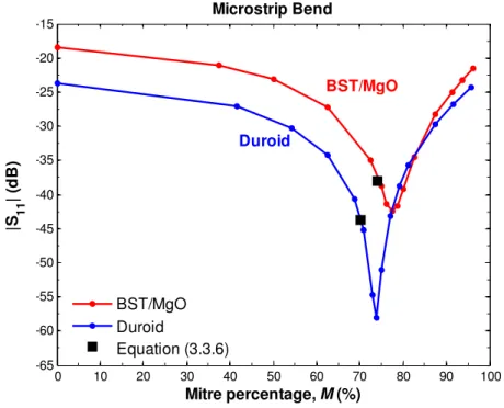
Figure 3.3.4: Right-angle microstrip bend (a) current distributions (b) equivalent circuit...37
Figure 3.3.5: Mitred right-angle microstrip bend (a) current distributions (b) equivalent circuit...38
Figure 3.3.6: Optimum mitre percentage as a function of normalised line width [82]. ...39
Figure 3.3.7: Simulated S11 of a 50 Ω microstrip bend as a function of mitre percentage M. (BST/MgO: w=400µm, h=500.35µm); (Duroid: w=240µm, h=254µm)...41
Figure 3.3.8: Unequal-impedance microstrip tee-junction (a) current distributions (b) equivalent circuit (impedance ratio 1: 2 : 2). ...42 Figure 3.3.9: Mitred unequal-impedance microstrip tee-junction (a) current distributions (b)
equivalent circuit (impedance ratio 1: 2 : 2)...42
Figure 3.3.10: Simulated S11 and S22 of unmitred (dotted line) and mitred (solid line) microstrip tee-junction on BST/MgO (w1=400µm, w2=140µm, a=368µm), and Duroid substrate (w1=240µm, w2=90µm, a=212µm). ...43
Figure 3.4.1: CPW configuration...44
Figure 3.4.2: Multilayer CPW configuration...45
Figure 3.4.3: CBCPW configuration. ...46
Figure 3.4.4: Multilayer CBCPW configuration. ...47
Figure 3.4.5: Dielectric loaded CBCPW configuration...48
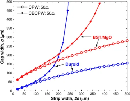
Figure 3.4.6: The strip width versus gap width curves for 50 Ω CPW and CBCPW...49
Figure 3.5.1: Layout of taper structure via-less CBCPW-to-microstrip transition...52
Figure 3.5.2: Simulated scattering-parameters of back-to-back CBCPW-to-microstrip transition on BST/MgO (solid line) and Duroid (dotted line) substrate...54
Figure 3.6.1: Calculated conductor, αc and dielectric loss, αd for CPW line on BST/MgO substrate with different strip widths. (g=54µm) ...58
Figure 3.6.2: Calculated conductor loss for CPW and CBCPW line on BST/MgO substrate with different strip widths. (g=54µm)...59
Figure 3.6.3: Illustration of the signal paths in the slots of a CPW line. The transient signals in the two slots are asynchronous after travelling through (a) a single bend, but may be synchronised again after passing through (b) the pair of oppositely oriented bends [98].60 Figure 3.6.4: Dominant modes in a CBCPW structure with infinite-width in-plane ground and finite-width substrate. (a) CPW mode, (b) parallel-plate mode [75]...62
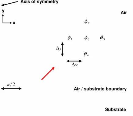
Figure 4.2.1: Illustration of mesh points on the cross-sectional microstrip line. ...66
Figure 4.2.2: Equal-arm grid mesh points...68
Figure 4.2.3: Unequal-arm grid mesh points. ...68
Figure 4.3.1: Illustration of mesh points on the boundary. ...70
Figure 4.3.2: Illustration of contour c for calculation of capacitance [110]. ...74
Figure 4.3.3: Approximated and experimental BST dielectric constant curve with respect to applied electric field adopted from [41]...77
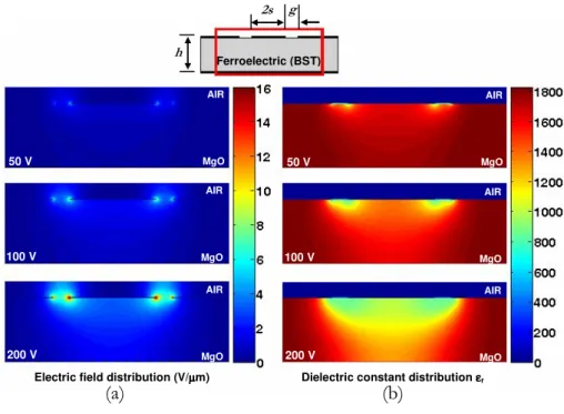
Figure 4.3.4: (a) Electric field and (b) dielectric constant distribution of a cross-sectional BST microstrip with 100V or 200V applied voltage...79
Figure 4.3.5: (a) Electric field and (b) dielectric constant distribution of a cross-sectional BST/MgO microstrip with 100V or 200V applied voltage. ...79 Figure 4.3.6: Enlarged view of the (a) electric field and (b) dielectric constant distribution of a
BST/MgO microstrip around the centre conductor at 200V...80 Figure 4.3.7: Computed characteristic impedance against w/h for microstrip on a layer of
isotropic BST at 300 K (h=100µm, V=200V). ...82 Figure 4.3.8: Convergence of residuals in the mesh grids for Duroid microstrip...83
Figure 4.3.9: (a) Electric field and (b) dielectric constant distribution of a cross-sectional BST CPW with various applied voltage. ...85
Figure 4.3.10: (a) Electric field and (b) dielectric constant distribution of a cross-sectional BST CBCPW with various applied voltage...85
Figure 4.3.11: Enlarged view of (a) electric field and (b) dielectric constant distribution of a cross-sectional BST/MgO CPW around the centre conductor with various applied voltages..86
Figure 4.3.12: Enlarged view of (a) electric field and (b) dielectric constant distribution of a cross-sectional BST/MgO CBCPW around the centre conductor with various applied voltages. ...86
Figure 5.2.1: CPW phase shifter based on BST thin-film and MgO substrate...93
Figure 5.2.2: Tapered CPW phase shifter with narrower strip and gap width, based on BST thin-film and MgO substrate. ...93
Figure 5.2.3: Measured (a) scattering-parameters, and (b) phase of CPW phase shifter with various bias voltages. ...96
Figure 5.2.4: Measured (a) scattering-parameters, and (b) phase of tapered CPW phase shifter with various bias voltages. ...97
Figure 5.2.5: Differential phase shift as a function of bias voltage for CPW and tapered CPW phase shifter. ...99
Figure 5.2.6: Differential phase shift as a function of frequency for CPW and tapered CPW phase shifter. ...99
Figure 5.2.7: Figure-of-merit of CPW phase shifter (dotted line) and tapered CPW phase shifter (solid line) with different bias voltages. ...100
Figure 5.2.8: Real part of the dielectric constant of BST thin-film and relative tunability of the BST thin-film as a function of applied electric field. 3 and represent the data extracted from CPW and tapered CPW phase shifter, respectively. ...102
Figure 5.2.9: Characteristic impedance as a function of bias voltage for CPW and tapered CPW phase shifter. ...102
Figure 5.2.10: Effective loss tangent tan δeff, as a function of frequency...103 Figure 5.2.11: Comparison of measured (solid lines) and simulated (dashed lines) (a) scattering-parameters, and (b) phase of the CPW phase shifter at various bias voltages...105
Figure 5.2.12: Comparison of measured (solid lines) and simulated (dashed lines) (a) scattering-parameters, and (b) phase of the tapered CPW phase shifter at various bias voltages. ..106
thin-film dielectric constant, ε′BST. 3 and represent the values used in the Sonnet simulations of CPW and tapered CPW phase shifter, respectively. ...108
Figure 5.3.1: Cross-section of CBCPW phase shifter based on (a) BST, and (b) Duroid substrate. ...110
Figure 5.3.2: Layout of the meandered CBCPW phase shifter. ...111
Figure 5.3.3: Simulated (a) scattering-parameters, (b) differential phase shift, and figure-of-merit of CBCPW phase shifter based on BST and MgO substrate with different bias voltages. ...113
Figure 5.3.4: Cross-section of CBCPW configuration based on Duroid substrate and loaded with top-substrate (a) in ideal case, and (b) with air gap layer between top-substrate and conductors...114
Figure 5.3.5: Simulated (a) scattering-parameters, (b) differential phase shift, and figure-of-merit of CBCPW phase shifter based on Duroid substrate and various top-substrate...116
Figure 5.3.6: Differential phase shift of CBCPW phase shifter based on Duroid substrate as a function of air gap thickness at 6 GHz. ...117
Figure 5.3.7: Simulated (a) scattering-parameters, (b) differential phase shift, and figure-of-merit of CBCPW phase shifter based on Duroid substrate with 8 µm thick of air gap...118 Figure 6.1.1: Schematic diagram of the tunable attenuator...123
Figure 6.1.2: Cross-section of tunable attenuator based on (a) BST substrate and (b) Duroid substrate...124
Figure 6.2.1:Two-way, equal- split Wilkinson power divider. ...126
Figure 6.2.2: Ideal scattering-parameter responses of a two-way equal-split Wilkinson power divider. Port 1 is the input port; Port 2 and 3 are the output ports. ...128
Figure 6.2.3: Layout of two-way, equal-split microstrip Wilkinson power divider...129
Figure 6.2.4: Simulated scattering-parameters of a two-way equal-split Wilkinson power divider in microstrip form on BST substrate. ...130
Figure 6.2.5: Simulated scattering-parameters of a two-way equal-split Wilkinson power divider in microstrip form on Duroid substrate. ...130
Figure 6.3.1: Generic device layout of the tunable attenuator...132
Figure 6.3.2: Ideal attenuation response of the tunable attenuator with respect to the phase difference between phase shifter A and B. ...133
Figure 6.3.3: Layout of the ferroelectric tunable attenuator on BST thin-film and MgO substrate. ...136
Figure 6.3.4: Simulated (a) S11, and (b) S21 of the BST-based tunable attenuator with various bias voltages on phase shifter A and zero bias on phase shifter B in lossless conditions. ....138
Figure 6.3.5: Simulated (a) S11, and (b) S21 of the BST-based tunable attenuator with various bias voltages on phase shifter A and zero bias on phase shifter B in lossy conditions...139
Figure 6.3.6: Layout of the Duroid-based tunable attenuator. ...140
Figure 6.3.7: Photograph of the fabricated Duroid-based tunable attenuator device. ...141
Figure 6.3.8: Attenuator-under-test in a cryogenic probe station connected to Agilent PNA network analyser E8361A...141
Figure 6.3.9: Photograph of the fabricated Duroid-based tunable attenuator device with phase shifter B loaded with a layer of top-substrate...143
Figure 6.3.10: A weight is placed above the top-substrate on phase shifter B...143
Figure 6.3.11: Measured (a) S11, and (b) S21 of the tunable attenuator based on Duroid substrate with similar top-substrate on both phase shifters (εA=εB). Solid and doted lines denote with and without the used of a weight, respectively...144
Figure 6.3.12: Measured (a) S11, and (b) S21 of the tunable attenuator based on Duroid substrate with bare phase shifter A and different top-substrate on phase shifter B (εA=1 and εA≠εB). Solid and doted lines denote with and without the used of a weight, respectively. ...146
Figure 6.3.13: Comparison of measured and Sonnet simulated scattering-parameters of the Duroid tunable attenuator with (a) similar top-substrate on both phase shifters (εA=εB), and with (b) bare phase shifter A and different top-substrate on phase shifter B (εA=1 and εA≠εB). ...147 Figure 6.3.14: Measured output phase of the Duroid-based tunable attenuator for various
combination of εA and εB.. ...149 Figure 6.3.15: Differential phase shift of the output signal for various combination of εA and εB. ...149 Figure B.1: Recession of the conductors of CBCPW for loss calculation using incremental-inductance method [98]...161
C capacitance
R resistance
L inductance
ε
r relative dielectric constantε
eff effective dielectric constantµ
0 permeability of free spacec0 speed of light in free space
E electric field
n tunability
nr relative tunability
tan
δ
dielectric loss tangentQ quality factor
K commutation quality factor
Zc characteristic impedance
FoM figure-of-merit
∆Φ differential phase shift
K(k) complete elliptic integral of the first kind
w strip width
g gap width of a coplanar line
s half width of a coplanar line centre strip
GW in-plane ground width of a coplanar line
h substrate thickness
t conductor thickness
σ
conductivityα
c attenuation due to conductor lossα
d attenuation due to dielectric lossα
r attenuation due to radiation lossRs surface resistance
δ
skin depthω
angular frequencyγ
complex propagation constantLIST OF ABBREVIATIONS
Al2O3 alumina (sapphire)
Au gold
Ba barium
BST barium strontium titanate
BTO barium titanate
CBCPW conductor-backed coplanar waveguide
CPW coplanar waveguide
Cu copper
DC direct current
EM electromagnetic
FDM finite difference method
FEM finite element method
FET field-effect transistors
GaAs galium arsenide
HTS high temperature superconductor
LaAlO3 lanthanum aluminate
LRRM load-reflect-reflect-match
MEMS micro-electro-mechanical systems
MgO magnesium oxide
MMIC monolithic microwave integrated circuit
MSL microstrip-like mode
PIN positive intrinsic negative
PLD pulse laser deposition
Q-factor quality factor
RF radio frequency
Si silicon
S-parameters scattering-parameters
Sr strontium
STO strontium titanate
TEM transverse electromagnetic
Chapter 1
Introduction
1.1
Motivation
There has been rapid growth in communication systems including satellite, 3G wireless phones, ultra-wide band and optical networks over the last few decades. Numerous frequency standards have coexisted in different parts of the world, along with an increasingly congested spectrum in the microwave frequencies. Hence, in recent years, there has been an immense interest in developing frequency-agile microwave devices to allow multi-band or multi-bandwidth operation with little impact on the component count. The trend towards these frequency-agile applications often demands high-speed, light-weight, low-operation voltage, compact and miniaturised of devices at a lower cost with high tunability, low loss and low power consumption [1-4].
Ferroelectric materials have been found to be particularly important materials for the development of electrically tunable devices since the 1960s [5-7]. The change in the dielectric constant of ferroelectric materials as a function of electric field is the
key to a wide range of applications. Examples in the field of microwave engineering are tunable resonators, frequency-agile filters, varactors (also known as variable or tunable capacitors), variable power dividers/combiners, variable-frequency oscillators, delay lines and shifters. The latter is the key component in phase-array antennas [8-11].
To the best of author’s knowledge, to date, no work on tunable attenuators using ferroelectric materials has been done; where as other ferroelectric-based tunable microwave devices have been studied extensively. Hence, the main objective of this work is to present a novel tunable attenuator device based on Barium Strontium Titanate (BST) ferroelectric thin-film. Alongside this, work on how the finite difference method, a computational technique, is modified to suit the evaluation of the cross-sectional field distribution of a ferroelectrics-based transmission line will be presented.
1.2
Competing Technologies for Tunable
Microwave Devices
Traditionally, tuning is done manually or mechanically. Fox [12] proposed the first manually adjustable waveguide phase shifter in 1946. Mechanical circuits are inexpensive, easy to fabricate and have very low loss with good power handling capability. However, they come in large sizes and have rather slow response speed and are therefore cumbersome. Today, many circuit technology options are available whose tunable performance is closely related to the choice of technology. These options essentially include semiconductors, micro-electro-mechanical systems (MEMS), ferrites and ferroelectric materials. The following section will briefly review these technologies and put emphasis on interesting possibilities offered by the use of ferroelectric thin-film materials.
1.2.1
Semiconductors
Semiconductor switching elements such as field-effect transistors (FET), positive intrinsic negative (PIN) diodes and varactor diodes were first introduced in tunable circuits in 1960s [13, 14] and are still the dominant devices for making tunable circuits [15-17]. Advantages they offer are their low cost and compactness and their faster switching speeds, in the order of tens to few hundreds of nanoseconds. In addition, they can be easily integrated with monolithic microwave integrated circuits (MMICs). The main drawback of semiconductors in tuning applications is their low quality factor at microwave frequencies and typically higher insertion loss. Moreover, semiconductors are highly non-linear and have a lower power handling capability. The non-linear response of semiconductors can be of great importance as it is the source of inter-modulation distortion [18].
1.2.2
MEMS
In the early 1990s, interest has emerged in micro-electro-mechanical systems (MEMS) where tunability is obtained by the physical movement of a component which usually changes the capacitance of the device. These devices use electrostatic [19, 20], piezoelectric [21] or thermal effects [22] to produce the movement. In general, MEMS devices offer considerable advantages over semiconductors in terms of performance, power handling capability and power consumption at the expense of slower switching speed. Typical switching speed is in the range of a few to tens of microseconds [23].
Despite a tremendous effort invested in the development of MEMS in the past few decades, the widespread use of MEMS has been impeded by the high cost of packaging and by reliability and lifetime testing issues. MEMS-based devices typically require hermetic packaging as the moving parts of the device tend to be very sensitive to the environmental conditions, such as air moisture, temperature and vibration [23, 24]. This significantly increases the cost over other technologies.
1.2.3
Ferrites
Another technology for making tunable microwave devices is the use of agile materials. Among them, ferrites have been found interesting for their change in permeability with an applied DC magnetic field. The first electronically variable ferrite phase shifter was reported in 1957 [25, 26]. Unfortunately, ferrite-based circuits are generally large, heavy, low switching speed and have high power consumption. In addition, tunable ferrite devices are difficult to integrate with planar circuits such as microstrip and stripline. Although ferrite-based devices are bulkier, their excellent tuning factor and power handling capability remain unsurpassed [25, 26]. The switching speed is in the order of tens of microseconds.
1.2.4
Ferroelectrics
Ferroelectric materials have been studied since the early 1960s in the field of microwave engineering [5-7]. However, it is only relatively recently that the applications in microwave devices are beginning to emerge. This recent renewed interest is due to the monolithically compatible processing of certain ferroelectric thin-film compounds with planar technologies [4, 27]. This has generated great interest and shows promise for the design of a new class of tunable microwave devices which could significantly reduce the cost of production. Contrary to ferrite devices, ferroelectric material-based devices take advantage of the property of the change in dielectric constant of ferroelectric material with an applied DC electric field. The dielectric constant and breakdown voltage of ferroelectric thin-films are intrinsically high, thus allowing increased miniaturisation and high power handling [2, 28]. Ferroelectric-based devices are tuned much faster than ferrite, semiconductors or MEMS type equivalents (< 1 ns) and have a near zero power consumption, but suffer from lower quality factor than MEMS [15, 24].
1.3
Comparison of Competing Technologies
Various technologies mentioned in the previous section have been used for many frequency-agile devices. All have their pros and cons. Therefore, the choice of technology strongly depends on the application, in terms of system specification, cost, ease of integration with other technologies and reliability. A comparison of various competing technologies in light of the parameters typically considered in system design, namely tunability, quality-factor (Q-factor), power consumption, switching time and power handling capability, is shown in Table 1.3.1. The entries reflect data from different literatures [15, 23, 24, 28-31], appropriate to general-purpose, continuously variable varactors and phase shifters, are suitable for microwave operation in a wide assortment of applications.Semicond. MEMS Ferrite Ferroelectric Tunability High Low Very High Moderate to
High Q-Factor Moderate 30-60 Very High 100-1000 High 50-100 Moderate < 100 Power Consumption Low < 10 mWa 0.05-0.1 mWb Low << 1 µW High ~10 W Low << 1 µW Switching Time Fast 1-5 nsa 2-10 nsb Slow 2-40 µsc 200-3000 µsd Moderate 10-100 µs Very Fast < 1 ns Power Handling High tens of watts Low < 50 mW Very High in kW High > 1 W Table 1.3.1: Comparison of various competing technologies [15, 23, 24, 28-31].
(a PIN Diode; b FET; c Electrostatic type; d Thermal/magnetic type)
Ferroelectric materials are favoured for applications which require rapid, continuous tuning and low power consumption as they work using an electric field.
In addition, ferroelectric-based devices are extremely competitive in terms of cost, weight and size, in particular at millimetre wavelength, without a significant sacrifice in performance for many applications, hence making them an excellent candidate for low cost frequency-agile devices.
1.4
Thesis Overview
This thesis presents work done on a novel tunable attenuator device which based on a Barium Strontium Titanate (Ba0.5Sr0.5TiO3 or BST) ferroelectric thin-film
on a Magnesium Oxide (MgO) substrate. A number of contributions to the field have been made during the course of this work. To the best of author’s knowledge, no work on tunable attenuators based on ferroelectric thin-films has been reported to date. The tunable attenuator in this work is realised into one integrated planar circuit. The properties of the ferroelectric materials (i.e. high dielectric constant) have allowed a significant reduction of device dimensions, weight and cost in mass production. Tunable attenuators has been previously designed using semiconductor tunable varactors in a cascade manner in order to achieve controlled attenuation in a similar piece of work [32]. However, the fabrication process was complicated and time consuming as the device required several layers of metallisation and substrates.
Ferroelectric materials have a non-linear dielectric constant which varies with the application of electric field and this is the key to many frequency-agile and tunable microwave devices. Chapter 2 reviews the fundamentals of ferroelectric materials and various methods of growing and characterisation techniques. This is followed by a brief survey of the ferroelectric-based frequency-agile devices reported in the literature.
Chapter 3 reviews various types of planar transmission lines, namely microstrip, coplanar waveguide (CPW) and conductor-backed coplanar waveguide (CBCPW). Crucial to circuit design, the closed form expression for the effective dielectric constant
ε
eff and characteristic impedance Zc of each geometry incorporatedwith ferroelectric material is presented. These expressions are derived using conformal mapping techniques where a quasi-static TEM (transverse electromagnetic) mode of propagation along the line is assumed. This section is supported by Appendix A and B, which presents the approximations used in the conformal mapping techniques and the steps involved in deriving the associated conductor loss of CBCPW, respectively.
Chapter 4 discusses the work on how the finite difference method (FDM), a computational technique, is modified to suit the evaluation of the cross-sectional field distribution of a ferroelectric-based transmission line. The derivation of the modified FDM is presented, together with the comparison of modified FDM with present closed form expression in finding
ε
eff and Zc for various types of transmission line. A paper has been published [33] in regards to this chapter and can be found in Appendix C.The fabrication and experimental measurement of CPW phase shifters which based on BST ferroelectric thin-films and MgO substrate are presented in Chapter 5. A DC bias voltage of up to 100 V is applied across the phase shifters which produced a phase shift of 105° at 20 GHz with an insertion loss of about 10.6 dB, giving a figure-of-merit of 14°/dB. The BST thin-films showed a tunability of ~48% at 3.13 V/µm. This work is carried out as a preliminary step towards using BST ferroelectric thin-films for designing CBCPW phase shifters, which are key components in the tunable attenuator described in Chapter 6. The design and the associated simulated response of CBCPW phase shifters are shown.
Chapter 6 presents the application of the BST ferroelectric phase shifter in a tunable attenuator. This novel topology of tunable attenuator that based on BST ferroelectric thin-films on an MgO substrate demonstrates a continuous variation of attenuation by appropriate control of DC bias voltage. A new design technique has been developed employing the principle of constructive and destructive interference by integrating two tunable phase shifters in parallel to produce attenuation of the signal. The simulation results of the BST tunable attenuator are shown.
In order to verify the simulation results as well as the validity of the operation principle of the BST tunable attenuator, a similar design of tunable attenuator which based on a dielectric substrate of dielectric constant 10.2 is designed and fabricated. The comparison of experimental and simulation results is shown.
Finally, Chapter 7 draws a close to this thesis with a summary and conclusions of the work done. The main findings and the limitations of this work are summarised. The application prospects of the presented tunable attenuator are addressed. Some suggestions of improvements and recommendations for future work are given.
1.5
Conclusions
In this introductory chapter, the motivation for this work was discussed. Various technologies in achieving frequency-agility in tunable microwave devices were reviewed and compared. Finally, an overview of the thesis was given. The next chapter presents the fundamentals of ferroelectric materials in terms of dielectric properties, various forms of ferroelectric materials and thin-film growing techniques. Literature on frequency-agile device using ferroelectric materials will also be discussed.
Chapter 2
Ferroelectric Materials and
Tunable Microwave Devices
2.1
Introduction
Ferroelectrics have been studied since the early 1960s for application in microwave engineering [5-7]. The change in the dielectric constant of ferroelectrics as a function of applied electric field is the key to a wide range of applications. Examples in the field of microwave engineering include tunable resonators, frequency-agile filters, varactors, variable power dividers/combiners, variable-frequency oscillators, delay-lines and phase shifters. The latter is the key component in phase-array antennas.
and, where available, single crystals. The initial idea of utilising bulk ferroelectrics in tunable microwave devices was not very successful as very high voltage is required to achieve a usable tuning range [4, 34]. Furthermore, integration of bulk ferroelectrics in devices is cumbersome. Whilst these materials have proved a robust and reliable solution, producing thin layers or dimensional tolerances better than a few microns has proved impractical [27].
However, there has been a renewed interest in application of ferroelectrics for tunable microwave devices since the 1980s [35]. This resurgent interest is largely due to the advances in thin-film growth techniques and the ability to integrate ferroelectrics with semiconductor and ceramic technologies, and thereby dramatically reduce the cost of the devices.
2.2
Ferroelectric Materials
Ferroelectric materials belong to a class of perovskite oxide materials that exhibit a spontaneous electric polarisation below the Curie temperature Tc. Upon cooling, there is a transition from the paraelectric to the ferroelectric state at Tc, where the maximum dielectric constant is observed. At temperatures below Tc (i.e. in ferroelectric state), a spontaneous electric polarisation is present where there is a relative displacement of ions in ferroelectric materials; this results in a net dipole moment. The orientation of the dipole moment in a ferroelectric can be shifted from one orientation to another under the influence of an applied electric field, causing a change in the dielectric constant of the material [2, 15, 34, 36]. The relation between polarisation and applied electric field is represented by the hysteresis curve shown in Figure 2.2.1. In the ferroelectric state, the polarisation of ferroelectrics remains even in the absence of an applied electric field. In the paraelectric state, there is only polarisation with the application of an external electric field.
Examples of ferroelectric materials are Barium Titanate (BaTiO3) and Barium
Strontium Titanate (BaxSr1-xTiO3 or BST). Figure 2.2.2 shows the perovskite structure
Figure 2.2.1: Polarisation of ferroelectric material in ferroelectric and paraelectric state in response to external applied electric field, showing
(a) hysteresis, and (b) no hysteresis.
external electric field. An operating temperature slightly above the Curie temperature in the paraelectric phase is normally preferred for tunable microwave devices as ferroelectrics in this state are free from the hysteretic effect and have moderate loss [15, 34]. Despite this technical distinction, ferroelectrics used in the paraelectric phase for tunable microwave devices are still referred to as ferroelectric materials.
2.2.1
Dielectric Properties
Ferroelectrics are essentially a non-linear dielectric due to their dielectric constant dependency with external applied electric field and temperature.
2.2.1.1
Field Dependent Dielectric Constant
Several ferroelectric materials are suited for integration with monolithic microwave integrated circuits (MMICs) and perhaps the most studied material for microwave application is BaxSr1-xTiO3 (BST), where x can vary from 0 to 1. BST is a
Electric Field Electric Field
Polarisation Polarisation
FERROELECTRIC PARAELECTRIC
Figure 2.2.2: Perovskite structure and electric polarisation of a unit cell Barium Strontium Titanate (Ba,Sr)TiO3 in response to external applied electric field [37].
No electric field
Direction of applied electric field
Ba, Sr O Ti
composition where Barium (Ba) ions are introduced into pure Strontium Titanate (SrTiO3 or STO) to attempt to improve the microwave properties. Pure STO is
particularly attractive due to its crystalline compatibility with high temperature superconductors (HTSs) and it is in the paraelectric state at all temperature, hence, there is no Curie temperature above 0 K. On the other hand, Barium Titanate (BTO) has a Curie temperature of about 400 K. Different composition ratio allows tailoring of the Curie temperature. Generally, a value of x = 0.4 – 0.6 is used to optimised its properties for room temperature, and a value of around x = 0.1 – 0.2 is used when the material is used in conjunction with HTS films [1, 2, 38-40].
Figure 2.2.3: Dielectric constant curve of a BST thin-film at 80 K and 300 K, adopted from [41]. and 3 represent the dielectric constant when voltage was swept up and down, respectively in order to demonstrate any hysteresis behaviour.
Figure 2.2.3 depicts the variation of the relative dielectric constant
ε
r of Ba0.5Sr0.5TiO3 (BST) thin-film as a function of electric field and temperature [41]. Asshown in the figure, the dielectric constant of BST decreases with increasing electric field and temperate. At 300 K, BST thin-films have a
ε
r in the range of 1000-2000300 K 80 K
εεεε
r
-4 -3 -2 -1 0 1 2 3 4 2000 1800 1600 1400 1200 1000 600 400 200 E (V/µµµµm)with no hysteresis [41]. This show the thin-films are in the paraelectric state. As temperature cools down to 80 K,
ε
r drops to below 700 and hysteresis is observed as the voltage was swept up and down. This is expected as the BST thin-film is in the ferroelectric state.2.2.1.2
Tunability
As mentioned earlier, one of the most important properties of ferroelectric material is the strong dependence of their dielectric constant on external applied electric field E. This characteristic is commonly described by the tunability n, defined as the ratio of the dielectric constant of the material at zero electric field to its dielectric constant at non-zero electric field, as expressed by equation (2.2.1). The relative tunability nr in percentage is defined by equation (2.2.2).
( )
( )
E nε
ε
0 = (2.2.1)( )
( )
( )
0 100% 0 ⋅ − =ε
ε
ε
E nr (2.2.2)2.2.1.3
Loss Tangent
Ferroelectric materials, like any other dielectrics, commonly suffer from dielectric losses. To express this mathematically, the dielectric constant of ferroelectrics can be represented in complex form with both real
ε′
and imaginary partsε″
as follow." ' ε ε
ε = +j (2.2.3)
The imaginary part of the dielectric constant ε″ accounts for the loss factor, governed by the lag in polarisation upon application of the electric field and the
energy dissipation associated with charge polarisation. This loss factor is characterised by the ratio of the imaginary and the real part of the dielectric constant, which commonly known as loss tangent, tan δ.
( )
( )
Q 1 ' " tan = = ℜ ℑ =ε
ε
ε
ε
δ
(2.2.4)where Q is the quality factor of the material. Ideally, materials with high tunability and low loss tangent at microwave frequencies are greatly desired in the field of microwave engineering application. However, in conjunction with high tunability, most ferroelectrics possess high loss and temperature dependency as well [42, 43]. The correlation between the tunability and the loss tangent often forces designers to choose the material with the optimal trade-off between these two parameters for best device performance.
2.2.2
Bulk, Thick-Film and Thin-Film
Ferroelectrics come in several forms, namely bulk, thick-film and thin-film. Each of these forms has its pros and cons. Bulk ferroelectrics are usually in the 500-2000 µm range thickness. Due to their very high dielectric constant, typically in the order of few to tens of thousands, bulk ferroelectrics are useful in substantial size reduction of microwave devices. Bulk ferroelectrics have been used in many applications such as tunable dielectric resonators [44, 45], tunable filters [46, 47], varactors [48] and a lens antenna [49]. The major drawback of bulk ferroelectrics, however, is that very high tuning voltages, in the order of hundreds of volts to tens of kilovolts [4, 34], is required to achieve a usable tuning range. This greatly limits their use in tunable microwave devices. Nonetheless, as will be pointed out later, bulk ferroelectrics generally exhibits lower loss tangent values than other form of ferroelectrics.
thickness stipulation, they are usually of a polycrystalline form. Ferroelectric thick-films are considered a more practical form than bulk as substantially lower tuning voltage is required (few hundreds of volts). Furthermore, with the development of tape casting [11] or screen-printing technology [50], the production cost of thick-film has significantly decreased, hence, making thick-film a good candidate for cost-effective tunable device. Many tunable devices, such as phase shifters [50, 51], varactors [15, 52] and tunable filters [53] have demonstrated the use of thick-film. These results, though promising, are not as good as that obtained with thin-film in terms of tunability.
A thickness of less than 1 µm is often referred to as thin-film and they are usually more crystalline in nature being made from sputtering, laser ablation or other thin-film processing technique. Ferroelectric thin-films are very attractive for microwave tunable application due to their relatively low production cost and most importantly, low tuning voltage requirement, typically between 2 and 200 volts, depending on the thin-film composition and film thickness. The dielectric response of ferroelectric thin-films is usually different from that of bulk ferroelectric materials in terms of dielectric constant and tunability. According to the literatures [4, 34], the dielectric constant of the thin-films is usually lower and the loss tangent, tan δ is always higher than in their bulk or thick-film counterparts. Nonetheless, the much lower tuning voltage and other integration benefits still make ferroelectric thin-film a very feasible candidate in tunable microwave devices. The quality of the ferroelectric thin-films is also strongly depends on the substrates used for film deposition. Substrates such as Magnesium Oxide (MgO), Alumina or Sapphire (Al2O3), and Lanthanum Aluminate (LaAlO3) are often used as substrate in ferroelectric film-based components due to their low loss tangent and their good lattice matching with the film.
2.2.3
Thin-Film Growth Techniques
which has its merits and disadvantages. Generally, these techniques can be classified into three groups:
Physical vapour deposition (PVD) – this includes RF and magnetron sputtering, molecular beam epitaxy and pulsed laser deposition (PLD)
Chemical vapour deposition (CVD) – this includes metal-organic chemical vapour deposition (MOCVD) and atomic layer deposition (ALD)
Chemical solution deposition (CSD) – this includes sol-gel and metal-organic decomposition
Pulse laser deposition (PLD) has several characteristics that made it remarkably competitive in the complex thin-film arena as compared to other film growth techniques. The distinct attractive feature that makes PLD technique so favourable is its ability to preserve the stoichiometry of compound materials (i.e. the deposited film has the same chemical structure as the target material) [35, 54]. Furthermore, PLD technique offers simplicity of use, relatively high deposition rate and it is more economical than other deposition techniques. It is not the intention of this thesis to elaborate PLD technique in detail but rather to have a brief overview of the methodology.
2.2.3.1
Pulsed Laser Deposition
The Pulsed Laser Deposition (PLD) technique has been widely used to grow various thin-films and multi-layers of complex materials for many years. Although the PLD technique is unable to make uniform film coating on large scale wafers and for mass production, it still has appeal for many researchers for the fabrication of high-quality films of ferroelectric materials [35, 54].
As shown in Figure 2.2.4, PLD consists of a target holder and a substrate heater housed in a vacuum chamber. A high power pulsed-laser beam, used as an external energy source, is focused inside the vacuum chamber to strike a target of the desired composition. Material is then vaporised in the form of an ionised plume from
the target, resulting in thin-film growth on the substrate. This process can occur in ultra high vacuum or in the presence of a background gas, such as oxygen which is commonly used when depositing oxides to oxygenate deposited films.
Figure 2.2.4: Schematic of PLD system for deposition of thin-films [54].
2.2.3.2
BST Thin-Film
A great deal of works on ferroelectric BaxSr1-xTiO3 (BST) thin-films growth using the PLD technique has been reported over the years [38, 40, 55-58]. BST thin-films are considered to be one of the most promising candidates for tunable microwave devices because of their large nonlinearity of dielectric constants with the applied electrical field and the adjustable dielectric properties from different doping ratio of Strontium (Sr) and Barium (Ba). BST thin-films with x = 0.4 – 0.6 are typically used as they demonstrates a large electric field effect at room temperature.
The dielectric constant and the loss tangent are the two most important parameters affecting the practical applications of BST thin-films in tunable
Ionised Plume Target Laser Beam Substrate on holder Focussing Lens
microwave devices. These parameters strongly depend on the quality of the film as well as the substrate used for film deposition [56, 58]. Single crystal (001) MgO substrate is often selected for the growth of BST thin-films due to its excellent dielectric properties in terms of low loss tangent, and also, its good durability and low-cost compared to other substrates.
2.3
Applications of Ferroelectric Materials
Ferroelectric materials have been receiving tremendous attention over the past decade due to the increasing demand for smaller size, lighter weight, higher speed, lower cost and higher power capability frequency-agile components. The change of dielectric constant of ferroelectric materials with the applied electrical field holds the key to a wide range of application such as varactor, phase shifter and tunable filter. This section aims to give a brief overview of the application of ferroelectric, BST thin-film in particular.
2.3.1
Varactor
A varactor, also known as variable or tunable capacitors, is by far the simplest component that can be produced by ferroelectric materials. There are essentially two categories of thin-film varactors, namely, planar varactors and parallel-plate varactors, as shown in Figure 2.3.1, although they are some variations in the exact configurations in the literatures [4, 44, 59-62].
The parallel-plate varactors have the advantage of using the tunability of the film more efficiently and require a relatively small voltage for effective tuning (1-20 V) since the electric fields are better confined in the film as the bias voltage is applied across the film thickness. However, parallel-plate varactors involved a more elaborate process and require bottom electrode patterning. In addition, the electrodes in parallel-plate structure contribute to a higher loss than in the case of planar structure.
For planar varactors, the electric field is applied along the ferroelectric film across the gap. The electrodes need to be close together in order to maximise the field within the ferroelectric film. The capacitance value can be completely controlled by the metallisation patterns and geometrical parameters on one metal layer. An interdigital finger structure has been used to increase the tunability of the varactor [63-65]. Figure 2.3.2 shows an example of the layout of an interdigital varactor.
Figure 2.3.1: (a) Planar, and (b) parallel-plate varactor based on ferroelectric film [34].
Figure 2.3.2: Layout of the interdigital varactor on ferroelectric film [65].
Ferroelectric Film Electrode Electrodes Ferroelectric Film Substrate (a) (b)
The characteristic of a varactor is based on two main parameters: tunability of the varactor and the loss factor, tan δ of the ferroelectric materials. This is described as Commutation Quality Factor K [66], defined as
(
)
2 1 2 tan tan 1 δ δ ⋅ ⋅ − = n n K (2.3.1)where n is the tunability of the varactor as defined in equation (2.2.1), and 2 , 1 2 , 1 2 , 1
tanδ =ωC R is the loss tangent of the varactor, determined by the value of the capacitance C and the series resistance R at zero and non-zero electric field, (denoted by subscript 1 and 2), respectively.
2.3.2
Phase Shifter
The ferroelectric phase shifter is by far the most widely studied tunable ferroelectric component and hence, has been reported in many papers [1, 8-10, 38-40, 67, 68]. A phase shifter is simply a device that provides a shift in phase angle of a microwave signal without depreciating the magnitude. They play a crucial role in phased array antennas for wireless and satellite communications system.
A phased array refers to an antenna configuration, composed of a large number of elements that emit phased signals, which can be served by thousands of phase shifters, to form the beam. The phase shifters are used to electronically steer and control the position of the beam. Traditionally, phase shifters in phased array antenna system are constructed using ferrites which strong magnetic fields are required for tuning. Implementing ferrite phase shifters in phase arrays are extremely costly, bulky and heavy for commercial applications. In addition, ferrite phase shifters are slow to respond to control signals hence, cannot be used in applications where rapid beam scanning is required. For these reasons, the application of ferroelectric phase shifters in phased array antenna is greatly favoured due to their potential for better performance in terms of tuning speed and power handling
capability, as well as smaller size and lower cost.
Ferroelectric phase shifters can be classified into two categories, analogue and digital. Analogue ferroelectric phase shifters have a single analogue input control voltage, giving a theoretical infinite resolution. The simplest form of analogue ferroelectric phase shifter is the use of a simple coplanar line structure patterned on a ferroelectric thin-film coated substrate, as shown in Figure 2.3.3. This type of phase shifter can also be called a delay-line. The phase velocity of the electromagnetic wave travelling through the line is varied by controlling the external applied electric field as the dielectric constant of the ferroelectric thin-film changes depending on the magnitude of the electric field strength, thus producing the phase shift.
Figure 2.3.3: Layout and cross section of a ferroelectric delay-line type analogue phase shifter in double layer substrate coplanar waveguide structure [68]. Another method is by loading the transmission line with a ferroelectric varactor where the phase velocity of the electromagnetic wave can be continuously tuned by biasing the varactor, providing necessary phase shift (Figure 2.3.4) [59]. This is contrast to the previous case where the coplanar line is homogeneously loaded with ferroelectric film. Analogue ferroelectric phase shifters are low cost and a precise phase shift can be obtained with single analogue control voltage.
Ferroelectric Film Electrode
Substrate
Digital ferroelectric phase shifters have digital input signals, offering a limited resolution or a fixed phase shift (e.g. 45°, 90° or 180°) [69]. Figure 2.3.5 shows the layout of a digital reflection type phase shifter, which consist of a transforming circuit that is terminated by a coplanar 3-electrode capacitor. The advantage of the digital phase shifters is a better impedance matching with the 50 Ω external impedance and also lower amplitude modulation distortions [69].
Figure 2.3.4: Layout of a loaded-line phase shifter with BST varactor [59].
Figure 2.3.5: Layout of the 180° ferroelectric reflection type digital phase shifter [69].
Ground Ground Signal RF INPUT RF OUTPUT BST Varactor DC contact pad Blocking capacitors Microwave Input 3-electrode capacitor
The performance of the phase shifter is determined by the amount of phase shift ∆Φ and the insertion loss of the phase shifter in both states IL1,2 (i.e. zero and
non-zero electric field). This is commonly described as figure-of-merit FoM, expressed by the following equation [16].
(
dB)
2 1 ° ⋅ ∆Φ = IL IL FoM (2.3.2)For a phase shifter based on ferroelectric varactor and lossless non-tunable components, the FoM of the phase shifter then depends on the Commutation Quality Factor (K) of the ferroelectric varactor only, as defined in equation (2.3.1), and turns into [16]:
( )
⋅(
° dB)
=B m K
FoM (2.3.3)
where B(m) is the coefficient depending on the types of phase shifter. This is shown in Table 2.3.1.
Number of bits, m 1 2 3 4 >>1
( )
mB for a digital phase shifter 10.36 9.11 8.68 8.50 8.36
Bfor a analogue phase shifter 6.6
Table 2.3.1: Coefficient B(m) for the figure-of-merit of a digital or analogue phase shifter [16].
2.3.3
Tunable Filter
Tunable filters are a more recent frequency-agile component implemented using ferroelectric materials. They have been reported in [3, 70-73]. These filters have been demonstrated in microstrip, coplanar waveguide (CPW) or conductor-backed coplanar waveguide (CBCPW) structure. The characteristic of the tunable band pass filter is determined by two most important parameters: in-band insertion loss of the
filter in both states and the shift of the central frequency due to the tuning. The figure-of-merit of the tunable band pass filter FoMBPF can be expressed in the
following form [66]:
(
1)
2 1 2 1 01 02 dB 1 − ⋅ ⋅ ∆ ⋅ ∆ − = IL IL FoMBPF ω ω ω ω (2.3.4) where ω01,02 are the central frequencies of the filter, ∆ω1,2 are the band widths of thefilter and IL1,2 are the insertion loss of the filter at both states (i.e. zero and non-zero
electric field). An example of a tunable band-pass filter based on ferroelectric materials [73] is presented in Figure 2.3.6. The dielectric substrate of the filter consists of two layers: a 1 µm thick of BST film and a 0.5 mm thick of alumina/sapphire (Al2O3) substrate. The thickness of the copper microstrip is 4 µm. The ferroelectric capacitors are formed by gaps in the microstrip lines. A figure-of-merit of 0.34 dB-1 is obtained with a 150 V biasing voltage at room temperature.
Figure 2.3.6: (a) Layout and (b) cross section of a tunable filters on BST film [73].
Alumina BST Copper Ferroelectric Capacitor (a) (b)
2.4
Conclusions
The fundamentals of ferroelectric materials in terms of dielectric properties, various forms of ferroelectric material and thin-film growing techniques have been presented. A brief survey of ferroelectric-based frequency-agile devices reported in the literatures has been reviewed. Many works on BST tunable microwave devices has been reported over the years. BST thin-films are particularly attractive due to their large nonlinearity of dielectric constant with the applied electrical field and their adjustable dielectric properties from different doping ratio of Strontium (Sr) and Barium (Ba). This allows tailoring of device operation at various temperatures. Pulsed laser deposition (PLD) technique is often used to grow BST thin-film. Such a growth method has been widely used in many research laboratories.
In the next chapter, a review of microstrip and coplanar waveguide will be presented. As crucial to circuit design, analytical expression for each geometry relevant to the inclusion of thin ferroelectric layers will be shown.
Chapter 3
Planar Transmission Lines
3.1
Introduction
A number of planar transmission lines will be briefly reviewed in this chapter and in particular, models of single and multilayer configuration will be presented. These models will be employed in Chapter 5 and 6 to predict the properties of the ferroelectric thin-film, as well as the performance of the ferroelectric phase shifter and tunable attenuator.
3.2
Planar Transmission Line Overview
A planar transmission line has conducting metal strips that lie entirely in parallel planes. This implies that the characteristics of the planar transmission lines can be determined by considering the dimensions in single or multiple planes. Ease of fabrication by photolithographic and printed circuit technique allows it to be used for a wide variety of circuit components. Planar transmission lines have played a
leading role in the development of both microwave integrated circuits (MICs) and monolithic microwave integrated circuits (MMICs). Examples of the most commonly used planar transmission lines are shown in Figure 3.2.1.
Figure 3.2.1: Main types of planar transmission line (a) stripline, (b) microstrip, (c) coplanar waveguide (CPW), and (d) conductor-backed CPW (CBCPW).
A stripline consists of a conducting strip embedded in a dielectric medium between two ground planes (Figure 3.2.1(a)). This construction supports a pure transverse electromagnetic (TEM) propagation mode as the conductor strip is completely surrounded by the dielectric medium (i.e. homogenous dielectric). The presence of both top and bottom ground planes provides good isolation from other signals. From a fabrication standpoint, a stripline is not as easily fabricated compared to a microstrip and coplanar waveguide. In practice, a small air gap can occur between the substrates during the fabrication process which would introduce an inhomogeniety in the stripline dielectric, and is often the reason for unexpected spurious transmission line performance.
SIGNAL GROUND CONDUCTOR-BACKED GROUND SIGNAL IN-PLANE GROUND IN-PLANE GROUND SIGNAL GROUND GROUND SIGNAL IN-PLANE GROUND IN-PLANE GROUND (a) (b) (c) (d)
Apart from benefits on the fabrication front, microstrip is one of the most popular planar transmission lines, primarily due to its integration compatibility with other microwave devices. A microstrip consists of a thin layer of conducting strip constructed on a dielectric substrate with a ground plane at the bottom (Figure 3.2.1(b)). Unlike the stripline however, this geometry does not support a pure TEM wave as the dielectric substrate does not fill the air region above the strip. As a result of the open structure of the microstrip, the electromagnetic field or energy transmitted in the microstrip may be radiated into space or adjacent lines.
A mutual drawback for both the stripline and microstrip is that for a given substrate thickness, the line widths cannot be arbitrarily chosen for a certain characteristic impedance. Coplanar waveguide (CPW) of the type shown in Figure 3.2.1(c), on the other hand, offers some degree of freedom as the characteristic impedance is determined by the ratio of strip and gap width and is less dependent on substrate thickness. Therefore, by keeping an appropriate strip-to-gap ratio, different line widths can be chosen for a specific characteristic impedance [74]. As the ground of the CPW structure is in the same plane as the conducting strip, it eliminates the need for via holes during surface mounting of the microwave device. In addition, CPW features the lowest cross talk or interference levels from other signals among these three planar transmission lines due to the presence of the ground plane between any two adjacent lines. As a result, CPW circuits can be fabricated more compact than microstrip and stripline circuits, making it an ideal circuit structure for MIC, as well as MMIC applications.
Figure 3.2.1(d) depicts the conductor-backed coplanar waveguide (CBCPW), a modification of CPW. The additional lower ground plane of CBCPW provides several advantages in the construction of MMIC such as improved mechanical support to the substrate and to act as a heat sink for circuits with active devices. However, the introduction of the conductor backing could potentially establish an unwanted parasitic parallel-plate mode leakage between the upper in-plane and lower ground plane, depending on frequency, substrate thickness and dielectric constant [75].
Two substrate configurations will be implemented in the ferroelectric phase shifter and tunable attenuator in this work. The first is a multilayer substrate configuration, which consists of a layer of ~0.35 µm thick ferroelectric BST thin-film with dielectric constant, εr of 1800 at zero bias voltage on top of a 500 µm thick
MgO substrate (εr = 9.8). The second configuration is a single layer Duroid substrate
of thickness 254 µm with εr of 10.2. In the following sections, models of both the
single and multilayer configurations will be presented and subsequently be used for circuit design described in later chapters.
3.3
Microstrip
The general structure of a microstrip is illustrated in Figure 3.3.1. A conducting strip with a width w and a thickness t is constructed on a dielectric substrate that has a relative dielectric constant εr and a thickness h, and the bottom of the substrate is a
ground (conducting) plane.
Figure 3.3.1: Microstrip configuration.
Microstrip has its field lines distributed within two media – air above and dielectric below. For this reason, the microstrip structure is inhomogeneous and does not support a pure TEM wave. With the presence of the dielectric-air interface, the wave propagation velocity in a microstrip will not only depend on its material properties, i.e. the dielectric constant ε and the permeability µ, but also on the
w
t
h
εεεεphysical dimensions of the microstrip [76]. In microstrip, most of the electromagnetic (EM) field is concentrated between the strip conductor and the ground plane in the substrate. The field in the air region or fringing field components are usually much smaller compared to the main field (within the substrate below the strip). In this situation, the dominant mode in a microstrip behaves like a TEM mode, and thus, TEM transmission line theory is applicable. This is usually referred to as quasi-TEM approximation and is valid over most of the operating frequency ranges of a microstrip.
In the quasi-TEM approximation, the inhomogeneous dielectric-air media of microstrip is replaced by a homogenous dielectric material with an effective dielectric constant. Transmission characteristics of the microstrip, namely, the effective dielectric constant εeffand characteristic impedance Zc can then be obtained by using
quasi-static analysis [77]. With this technique, the fundamental mode of wave propagation in a microstrip is assumed to be pure TEM. This analysis was found to be adequate for designing circuits at frequencies below the X-band where the strip width and the substrate thickness are many orders of magnitude smaller than the wavelength in the dielectric materials [77].
For a single layer microstrip structure, as depicted in Figure 3.3.1, the closed-form expressions for εeff and Zc reported by [78] are given as follows.
ab r r eff u − + − + + = 1 10 2 1 2 1 ε ε ε (3.3.1) + + = 2 0 ln 1 2 2 u u F Z eff c
ε
π
η
(3.3.2) where u=w h, η µ ε 120π 0 0 0 = ≈ , and + + + + + = 3 4 2 4 1 . 18 1 ln 7 . 18 1 432 . 0 52 ln 49 1 1 u u u u a 053 . 0 3 9 . 0 564 . 0 + − = r r b
ε
ε
(
)
− − + = 7528 . 0 666 . 30 exp 6 2 6 u Fπ
In this single layer microstrip model, the thickness of the conductor is assumed to be very thin (i.e. t → 0). The accuracy of
ε
eff is better than 0.2% forε
r ≤ 128![Figure 2.2.4: Schematic of PLD system for deposition of thin-films [54].](https://thumb-us.123doks.com/thumbv2/123dok_us/655021.2578981/33.892.252.731.303.699/figure-schematic-pld-deposition-films.webp)
![Figure 2.3.5: Layout of the 180° ferroelectric reflection type digital phase shifter [69]](https://thumb-us.123doks.com/thumbv2/123dok_us/655021.2578981/38.892.242.720.676.1007/figure-layout-ferroelectric-reflection-type-digital-phase-shifter.webp)