University of Central Florida University of Central Florida
STARS
STARS
Electronic Theses and Dissertations, 2004-20192016
Stochastic-Based Computing with Emerging Spin-Based Device
Stochastic-Based Computing with Emerging Spin-Based Device
Technologies
Technologies
Yu BaiUniversity of Central Florida
Part of the Electrical and Computer Engineering Commons
Find similar works at: https://stars.library.ucf.edu/etd University of Central Florida Libraries http://library.ucf.edu
This Doctoral Dissertation (Open Access) is brought to you for free and open access by STARS. It has been accepted for inclusion in Electronic Theses and Dissertations, 2004-2019 by an authorized administrator of STARS. For more
information, please contact [email protected].
STARS Citation STARS Citation
Bai, Yu, "Stochastic-Based Computing with Emerging Spin-Based Device Technologies" (2016). Electronic Theses and Dissertations, 2004-2019. 5424.
STOCHASTIC-BASED COMPUTING WITH EMERGING SPIN-BASED DEVICE TECHNOLOGIES
by
YU BAI
M.S. University of Texas-Pan America, 2011 B.S. National Aviation University, 2008
A dissertation submitted in partial fulfilment of the requirements for the degree of Doctor of Philosophy
in the Department of Electrical Engineering and Computer Science in the College of Engineering and Computer Science
at the University of Central Florida Orlando, Florida
Summer Term 2016
c
ABSTRACT
In this dissertation, analog and emerging device physics is explored to provide a technology plat-form to design new bio-inspired system and novel architecture. With CMOS approaching the nano-scaling, their physics limits in feature size. Therefore, their physical device characteristics will pose severe challenges to constructing robust digital circuitry. Unlike transistor defects due to fabrication imperfection, quantum-related switching uncertainties will seriously increase their sus-ceptibility to noise, thus rendering the traditional thinking and logic design techniques inadequate. Therefore, the trend of current research objectives is to create a non-Boolean high-level compu-tational model and map it directly to the unique operational properties of new, power efficient, nanoscale devices.
The focus of this research is based on two-fold: 1) Investigation of the physical hysteresis switching behaviors of domain wall device. We analyze phenomenon of domain wall device and identify hys-teresis behavior with current range. We proposed the Domain-Wall-Motion-based (DWM) NCL circuit that achieves approximately 30x and 8x improvements in energy efficiency and chip layout area, respectively, over its equivalent CMOS design, while maintaining similar delay performance for a one bit full adder. 2) Investigation of the physical stochastic switching behaviors of Mag-netic Tunnel Junction (MTJ) device. With analyzing of stochastic switching behaviors of MTJ, we proposed an innovative stochastic-based architecture for implementing artificial neural network (S-ANN) with both magnetic tunneling junction (MTJ) and domain wall motion (DWM) devices, which enables efficient computing at an ultra-low voltage. For a well-known pattern recognition task, our mixed-model HSPICE simulation results have shown that a 34-neuron S-ANN imple-mentation, when compared with its deterministic-based ANN counterparts implemented with
ACKNOWLEDGMENTS
I would like to first sincerely thank my wife and parents for their endless love, support, and en-couragement. Secondly, I would like to thank my Ph.D. research advisor, Professor Mingjie Lin, for his patient guidance, encouragement, and support during my studies and research. I am truly fortunate to have him as an advisor, and any of the research in this dissertation would not have been possible without him.
I would also like to thank Prof. Ronald F. DeMara, Prof. Jun Wang, Prof. Yier Jin, and Prof. Yajie Dong for serving on the advisory committee and providing me with valuable comments and suggestions to improve my research.
TABLE OF CONTENTS
LIST OF FIGURES . . . ix
LIST OF TABLES . . . .xviii
CHAPTER 1: INTRODUCTION . . . 1
CHAPTER 2: BASIC PRINCIPLES OF SPINTRONICS DEVICE . . . 5
Introduction . . . 5
Two Terminal Magnetic Tunnel Junction . . . 5
Domain Wall Device . . . 7
Ferromagnetic Spin Orbit Torque Device . . . 10
CHAPTER 3: ULTRA-ROBUST NULL CONVENTION LOGIC CIRCUIT WITH EMERG-ING DOMAIN WALL DEVICES . . . 16
Introduction . . . 16
NCL Concept and Circuit Design . . . 18
Why All Spin Torque Null Convention Logic . . . 20
Transformation From Boolean NCL to Spin Torque NCL . . . 24
Proposed Asynchronous Circuit Design Through Magnetic Domain Wall NCL Gate . . . 32
The Performance Analysis and Discussion . . . 37
Large Scale Application of Proposed NCL Architecture . . . 40
Memristor error analysis . . . 43
Domain wall error analysis . . . 45
Conclusion . . . 45
CHAPTER 4: DESIGN OF STOCHASTIC ARTIFICIAL NEURAL NETWORK THROUGH EMERGING DEVICES . . . 47
Introduction . . . 47
Prior Work on ANN Hardware Implementation . . . 50
Why Stochastic-based ANN? . . . 52
Stochastic-Based Artificial Neural Network . . . 54
Stochastic Switching of MTJ and DWM Devices . . . 56
Stochastic-Based Synapse with STT Device . . . 59
Stochastic-based Soft-limiting Neuron . . . 66
S-ANN for Pattern Recognition:
Results and Performance . . . 71
Analytical Error Study . . . 78
Conclusion . . . 80
CHAPTER 5: SPIN-TRANSFER-TORQUE-DRIVEN AND NEURON-BASED FPGA AR-CHITECTURE WITH EMERGING DEVICES . . . 81
Introduction . . . 81
Architecture Overview of SN-FPGA . . . 85
MIMO-LUT: Idea and Methodology . . . 86
Algebraically Reinterpreting LUT . . . 88
MIMO-LUT with Artificial Neural Network . . . 90
MIMO-LUT: Circuit Implementation . . . 92
Spin-Transfer-Torque-based Artificial Neural Network . . . 92
All Spin Neural Synapse . . . 94
All Spin Neuron . . . 98
Final Piece: Flip-Flops . . . 101
Conclusion . . . 112
CHAPTER 6: CONCLUSION . . . 114
LIST OF FIGURES
Figure 1.1: (a). Exponential increase in power leakage of CMOS device. (b).
Tempo-ral degradation of performance of CMOS device [48]. . . 1
Figure 1.2: (a). CMOS device switching energy. (b). Spintronics device switching
energy. . . 2
Figure 2.1: Simplified Magnetic Tunnel Junction (MTJ) structure . . . 6
Figure 2.2: (a) Structure of an MTJ device[117]. (b) Our SPICE simulation results
of random signal generation. (c) Experimental and analytical results of switching probability vs. the pulse duration at different voltages [106, 39,
83]. . . 7
Figure 2.3: Schematic illustration of domain wall motion device. (a) Simplistic
con-ceptual view. (b) More realistic Three-terminal DWM cell structure. (b)
Equivalent circuital view. . . 8
Figure 2.4: (a) Simulation of domain wall moving by current injection in terminal T1,
the domain wall is moving to right by the spin polarized electrons. (b) Compact model presents good agreement with micromagnetic simulation
for DW motion speed V as a function of current densityjp [117]. (c). A
non-zero current inject to DW motion and obtains results in a hysteresis in
Figure 2.5: The physical phenomena of SHE assisted domain wall device. The domain wall is moving in PMA nanowires according to flow of in-plane injec-tion current through HM layer. The SOT coupling is generated and makes stabilization of chiral Neel domain wall through DMI. According to this model, a transverse spin current is generated by in-plane injection current.
The top and down view is shown in Fig. 2.5. . . 11
Figure 2.6: Schematic spin neuron device with spin torque layer. (a) Three-terminal
DWM cell structure. (b) DW speed with and without SHE assist. (c) DW switch characteristics. The hysteresis characteristics depends on critical
currentIcof DW moving. . . 13
Figure 2.7: Mumax3 simulation of DW motion according to injected current of25µA
flowing through the HM layer in 0.3ns. The given FM layer is 100nm in
length with ferromagnet thickness 0.6nm. . . 14
Figure 3.1: NCL overall scheme: input wavefronts are controlled by local
handshak-ing and completion detection signals. (a) Traditional NCL pipeline. (b) Symbol and structure of threshold gate TH23. (c) Implementation of logic
functionZ =X⊕Y. (d) Two-bit register and completion detector. . . 18
Figure 3.2: (a). Layout of single domain wall with 2 access transistor. (b). Layout of
two bit domain wall with 3 access transistor. . . 21
Figure 3.3: (a) TH23 static NCL gates. (b) TH23 DWL NCL gate. . . 22
Figure 3.5: (a) CMOS NCL THXOR gate (b) CMOS NCL THand0 gate (c) CMOS NCL TH24comp gate (d) Spin-torque-transfer DW device based NCL THXOR gate architecture (e) Spin-torque-transfer DW device based NCL THand0 gate architecture (f) Spin-torque-transfer DW device based NCL TH24comp gate architecture (g) Simulation of Spin-torque-transfer DW device based NCL THXOR gate architecture (h) Simulation of Spin-torque-transfer DW device based NCL THand0 gate architecture (i) Simulation of
Spin-torque-transfer DW device based NCL TH24comp gate architecture . . . 31
Figure 3.6: (a) Dual rail spin torque NCL architecture with reading scheme. (b)
Sim-ulation of NPN transistor with different supplied voltageVcc. The input
current is generated from DW sensing current and amplified through NPN
transistor. . . 32
Figure 3.7: (a). DWL duail rail NCL implementation, the two dual rail bits can be
implemented through two domain wall device which is separated by shared terminals. (b). The equivalence analog circuit of proposed DWL duail rail architecture in NULL case. (c). The equivalence analog circuit of proposed DWL duail rail architecture in DATA 1 case . (d).The equivalence analog circuit of proposed DWL duail rail architecture in DATA0 case. (e). The DWL dual rail 4-phase communication protocol. (f). DWL asynchronous QDI pipeline architecture, the input is controlled by local handshaking and
completion detection signal (ACK). . . 36
Figure 3.8: (a). DWL duail rail NCL architecture of one bit full adder. (b). CMOS
Figure 3.10: (a). Delay measurement of different selected TH gate. (b). Energy mea-surement of different selected TH gate. (c). Area meamea-surement of different
selected TH gate. . . 38
Figure 3.11: (a). Delay measurement of NCL full adder with increasing bits. (b). En-ergy measurement in log scale of NCL full adder with increasing bits.(c).
Area measurement in log scale of NCL full adder with increasing bits. . . 39
Figure 3.12: IEEE single precision floating point co-processor architecture [119]. . . 41
Figure 3.13: CAD flow of DWNCL simulation framework . . . 41
Figure 3.14: (a). Memristor refresh architecture, the refresh signal is controlled by in-puts of DW reset signal and acknowledge signal from next stage. (b). The
waveform of control signal inR/W control module. (c). The memristor
drift simulation of different input current with time increasing. (d). The memristor drift simulation of different pulse duration current with input
current increasing. . . 43
Figure 4.1: Structure of an artificial neuron. It consists of three computation blocks.
The weighted sum of all inputs are passed to its output through a transfer function. Four most common transfer functions are shown on right side of
Fig. 4.1. . . 48
Figure 4.2: Taxonomy of current ANN designs. Con: CMOS Technology; Em:
Figure 4.3: (a) MTJ device resistance histogram distribution of two statesRP andRAP
underσ/µ = 5%, 10%, and 25% of device resistance (b) Comparison of
weight variation on memristor based method and MTJ stochastic based
method . . . 52
Figure 4.4: Architecture of proposed stochastic neuron . . . 55
Figure 4.5: (a) Spin-torque-transfer DW device structure (b) Micro-magnetic
simu-lation of free layer DW motion when injected current density is 1.5×
1013A/m2 . . . . 57
Figure 4.6: Circuit design of random bit stream generation. (a) Configuration mode.
(b) Operation mode. Devices in gray area are active for each mode. Red curves depict signal directions. (c) HSPICE simulation of MTJ stochas-tic switching in 3 different devices which are programmed with different
probability values. . . 59
Figure 4.7: (a) Simulation of NPN transistor with different supplied voltagesVcc, where
the input current is generated from a DW sensing current and amplified through a NPN transistor (b) Simulation of a NPN transistor with different
parametersβ . . . 61
Figure 4.8: (a) The equivalent DW position used for generating corresponding
proba-bility through MTJ device (b) The equivalent writing current used to inject into DW device for generating corresponding probability through MTJ
de-vice . . . 62
Figure 4.10: Simulation results of proposed new stochastic weighted topology (a). Input bit stream of stochastic neuron (b). MTJ bit stream according to writing
current (c) Output bit stream . . . 63
Figure 4.11: Random number generation scheme of proposed architecture [46, 21]. . . . 64
Figure 4.12: HSPICE simulation of proposed architecture with writing and resetting
operation. . . 65
Figure 4.13: (a). The transfer function of ANN neuron (b). Architecture of proposed
stochastic-based linear transfer function neuron. . . 66
Figure 4.14: SPICE simulation of DW1 device receiving sum of input current pulse.
The 3 inputs current pulse with probability0.3,0.3,0.6is summed through
connecting in parallel. Different magnitude of current pulse leads to
dif-ferent DW speed. . . 67
Figure 4.15: (a)mumax3simulation of DW1 position and corresponding DW2 position
(b)mumax3 simulation of DW1 position and corresponding DW2 voltage
output (c)mumax3simulation of transfer function with different DW layers. 69
Figure 4.16: Overall Architecture of S-ANN. . . 70
Figure 4.17: CAD flow of S-ANN simulation framework . . . 71
Figure 4.18: (a) Architecture of a feed-forward ANN for hand written recognition tasks
(b) Output neuron voltage distribution, output neuronO1 has higher
volt-age than other output neurons when input pattern is A. (c) Normalized
in-put pattern and outin-put neuron, each block(i, j)indicatesjthwinner output
Figure 4.19: (a) Energy for different single neuron implementations. (b) Hidden layer
area based on different transfer functions. . . 73
Figure 4.20: (a) Input hand written image of A-Z alphabets (b) Input hand written im-age of ”ADJUSTMENT IS LIFE” (c) Input hand written imim-age of ”LIFE IS TOO COMPLICATED IN THE MORNING” (d) The comparison of number of pattern recognitions with two different methods for input image from (a) under increasing device variations (e) The comparison of number of pattern recognitions with two different methods for input image from (b) under increasing device variations (f) The comparison of number of pattern recognitions with two different methods for input image from (c)
under increasing device variations . . . 75
Figure 4.21: (a) The MSE simulation of stochastic bit stream with increasing of bit flip error rate both in analytical and simulation method. (b) The MSE simu-lation of stochastic bit stream with different probability both in analytical
and simulation method [19]. . . 77
Figure 4.22: Simulation of theoretical and simulated results. . . 78
Figure 4.23: Random bit stream error with different bit length. . . 78
Figure 5.1: (a) Cross-section of a MTJ-CMOS hybrid chip. (b) Monolithically stacked
3D-FPGA [73]. . . 81
Figure 5.2: (a) 2-D Island-style FPGA architecture. (b) SN-FPGA architecture with
Figure 5.3: (a) Logic diagram of a 4:2 encoder. (b) Truth table. (c) Encoded inputs
and outputs. (d) Logic curve interpretation. . . 89
Figure 5.4: Theoretical analysis of hardware usage of conventional (FPGA) method
and neural network method. . . 91
Figure 5.5: Structure of proposed ANN. The synapse, neuron and axon are
imple-mented through all spin device. . . 94
Figure 5.6: (a) Architecture of proposed synapse. (b) The equivalent circuit of
pro-posed synapse. The two reading currents flowing through two opposite devices and weighted by device conductance. The conductance is used to encode synaptic weight and program by DW position through writing
current. . . 95
Figure 5.7: Simulation results of proposed differential SHE domain wall architecture.
The difference of device conductance cause different combinations of
out-put reading current. . . 97
Figure 5.8: (a). Linear transfer function (b). Architecture of proposed adaptive soft
limit transfer function neuron. . . 98
Figure 5.9: (a)mumax3simulation of DW1 position and corresponding DW2 position
(b)mumax3 simulation of DW1 position and corresponding DW2 voltage
output (c)mumax3 simulation of adaptive DW soft limit neuron transfer
Figure 5.10: (a) Proposed analog flip flop architecture with SHE domain wall device and CMOS control logic. (b) Proposed flip flop operation time diagram. (c) Spice simulation of proposed analog flip flop according to time diagram Fig. 5.10. . . 102
Figure 5.11: Simulation results of proposed truth table approximation method. The C17 truth table is learned by proposed artificial neural network. Since the learn-ing process has different learnlearn-ing errors. In this paper, we select the best learning results. The random input number inputs to artificial neural
net-work and procedure correct output. . . 104
Figure 5.12: Customized CAD flow for SN-FPGA. . . 105
Figure 5.13: ABC synthesis results of four different benchmark circuit with different LUT size and output bits. The usage of multi-output bits will decrease the number of nodes dramatically. . . 106
Figure 5.14: The area comparison of different FPGA architecture[24, 27, 75] . . . 109
Figure 5.15: Delay comparisons between different FPGA architectures[24, 27, 75] . . . 110
LIST OF TABLES
Table 2.1: Device parameter used in simulation . . . 14
Table 3.1: One and two inputs mapping results of proposed Algorithm1 for 27 foun-dational NCL functions . . . 28
Table 3.2: Two and three inputs mapping results of proposed Algorithm1 for 27 foun-dational NCL functions . . . 29
Table 3.3: Four and five inputs mapping results of proposed Algorithm1 for 27 foun-dational NCL functions . . . 30
Table 3.4: Device simulation used in simulation of TH44 gate . . . 32
Table 3.5: Read current values for four states of proposed dual rail NCL architecture . 35 Table 3.6: Comparison of different design implementation for 32 bit IEEE single-precision floating point co-processor [119]. . . 42
Table 4.1: Domain wall device parameters. . . 58
Table 4.2: MTJ device parameter. . . 65
Table 4.3: Number of neurons with different transfer functions . . . 72
CHAPTER 1: INTRODUCTION
Although the research based on semiconductor has enjoyed for decades, the power performance, reliability and consumption of very large scale integration (VLSI) circuits are facing a large chal-lenge. On the performance part, the CMOS suffers from large leakage power consumption, slow switch speed, large size. These phenomena are more serious with CMOS down to nano-scale. On the reliability part, as nano-scale field-effect devices quickly approach their physical limits in fea-ture size, their stochastic device characteristics will pose severe challenges to constructing robust digital circuitry, shown in Fig. 1.1 [48].
In order to overcome these issues, there is a number of post-CMOS technology researches have been proposed [10]. It is obvious that the future IC will be composed of an amalgam of such emerg-ing technologies. The spintronics device is one of the promisemerg-ing devices, where the computation is based on the spin polarization of electrons.
Technology (
m
)
L
ea
kage
Pow
er
(% of
T
ota
l)
0% 10% 20% 30% 40% 50% 1.5 0.7 0.35 0.18 0.09 0.05Tech. generation
Fail
ure
p
ro
b
ab
il
it
y
Time
Defects
Life time
degradation
(a)
(b)
Figure 1.1: (a). Exponential increase in power leakage of CMOS device. (b). Temporal degrada-tion of performance of CMOS device [48].
MOS
ܧ ൎ ݔ݇ܶ GateMagnetic
Dissipated energy ൌ ͲǤͷܥܸଶ ൎ ܰ ȉ ܧ Dissipated energy ൎ ܧ(a)
(b)
Figure 1.2: (a). CMOS device switching energy. (b). Spintronics device switching energy.
Compared with CMOS, the spintronics device has a less switch energy. In Fig. 1.2, the comparison of switching energy with two different devices is measured. In Fig. 1.2 (a), the dissipated energy of
MOS device is calculated by using given parameters,N ≈10000andx = 40. The approximated
dissipated energy per switch is 1e−15J/switch. On the contrary, in Fig. 1.2 (b), the magnetic
displacement energy of spintronic device is obtained according to the equivalent collective entity,
N = 10 and x = 40. Therefore, the equivalent dissipated energy is1e−19J/switch with 7 years
lifetime. In conclusion, the spintronic device has a less switch energy than MOSFET (0.1aJ <<
1fJ) theoretically.
In general, for the applications of spintronic device, the digital states are represented by the orien-tation of magnetization in a ferromagnetic material with uniaxial anisotropy in spintronic devices. However, such spintronic devices are not drop in replacement for CMOS because of special device physical characteristics and variations. Compared with other approaches, which is trying to mini-mize spintronic device special physical characteristics and variations, we intend to unitize device physical characteristics to achieve native, robust and high performance computing.
In this dissertation, we propose three approaches based on our approach. The first approach uses emerging spintronic devices, this approach proposes a Domain-Wall-Motion-based NCL circuit design methodology that achieves approximately 30x and 8x improvements in energy efficiency
and chip layout area, respectively, over its equivalent CMOS design, while maintaining similar de-lay performance for a 32-bit full adder. These advantages are made possible, mostly by exploiting the domain wall motion physics to natively realize the hysteresis critically needed in NCL. More Interestingly, this design choice achieves ultra-high robustness by allowing spintronic device pa-rameters to vary within a predetermined range while still achieving correct operations. The second approach describes an innovative FPGA architecture attempting to exploit the physical phenom-ena newly found in emerging spintronic devices for bio-inspired reconfigurable computing. While many recent studies have investigated using Spin Transfer Torque Memory (STTM) devices to replace configuration memory in FPGAs, our study, for the first time, attempts to use the quantum-induced approximation property exhibited by spintronic devices directly for reconfiguration and logic computation. Specifically, the SN-FPGA was designed from scratch for high performance, routability, and ease-of-use. It supports variable granularity multiple-input-multiple-output logic blocks (MIMOLB), which has been purposely designed to conform with the standard K-LUT inter-face. As such, no major modifications need be made in the standard VPR placement/routing CAD flow. In the third approach, we propose an innovative stochastic-based architecture for implement-ing artificial neural network (S-ANN) with both magnetic tunnelimplement-ing junction (MTJ) and domain wall motion (DWM) devices, which enables efficient computing at an ultra-low voltage. For a well-known pattern recognition task, our mixed-model HSPICE simulation results have shown that a 34-neuron S-ANN implementation, when compared with its deterministic-based ANN counter-parts implemented with digital and analog CMOS circuits, achieves more than 1.5 to 2 orders of magnitude lower energy consumption and 2 to 2.5 orders of magnitude less hidden layer chip area. S-ANN architecture achieves such a remarkable performance gain by leveraging two key ideas. First, because all neural signals are encoded as random bit streams, the standard weighed-sum synapses can be accomplished by stochastic bit writing and reading procedure. Second, we de-signed and implemented a novel multiple-phase pumping circuit structure to effectively realize the
reduce its network complexity.
This dissertation is organized as follows: The basics of spintronic devices are reviewed in Chap-ter 2. By using hysChap-teresis physical characChap-teristics of Domain Wall Device (DWM), the robust
extra-low power DWM based NCL circuits are proposed in Chapter 3. In Chapter??, we proposed
stochastic artificial neural network according to stochastic switching physical behavior of Mag-netic Tunnel Junction (MTJ). In Chapter 5, we proposed bio-inspired reconfigurable architecture based on physical phenomena newly found in spintronics device. In Chapter 6, we summarize and concludes this dissertation.
CHAPTER 2: BASIC PRINCIPLES OF SPINTRONICS DEVICE
Introduction
This chapter describes basic principles of spinitronics devices. Firstly, we introduce the two ter-minal Magnetic Tunnel Junction (MTJ). Secondly, the three terter-minal DWM and MTJ devices are described. The detailed information of these spintronic devices is presented. The design parame-ters and impact on the application performance, density, and reliability are discussed. Furthermore, the explanation of the underlying physics involved with emerging device enables complex compu-tation native mapping of the single spintronic device is presented.
Two Terminal Magnetic Tunnel Junction
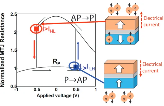
The Magnetic Tunnel Junction (MTJ) is two terminal spintronic device. It composed of two fer-romagnetic layers, free-layer (FL) and pinned-layer (PL), which are separated by a thin tunneling barrier (AlO or MgO). The pinned layer has fixed spin magnetization as reference layer. The mag-netization of the free layer can be switched by effecting of external factors such as magnetic field or spin polarized current 2.1. This bi-stable magnetization direction of the free layer is used to store binary information, which is either parallel (P) or anti-parallel (AP) to the fixed layer. Since the two states of binary information are separated by energy barrier, the system does not require a constant supply of power, called non-volatile device. In Fig. 2.1, the resistance difference is read out by applying a small read voltage (current). To write the binary information into the MTJ, a larger voltage is applied and generated writing current through the MTJ. The writing current direction determines the value of the data being written.
e e e e e e Electrical current e e e e Electrical current
AP
՜
P
P
՜
AP
Figure 2.1: Simplified Magnetic Tunnel Junction (MTJ) structure
Numerous studies have shown that emerging spintronic devices can exhibit complex switching behaviors due to the shifting of their intrinsic magnetic moment (spin) of electrons. For example, in magnetic tunneling junctions (MTJs) (depicted in Fig. 5.1 (a)) [120]. The switching characteristic of their spin-torque switching is highly stochastic and exhibits a well-defined probability as shown
in Fig. 5.1(b). Several recent studies have discovered that MTJ’s switching probability,Psw, mainly
depends on its intrinsic switching current and a thermal stability parameter (∆), where the ∆ =
Eu/kBT, Eu, kB, and T are uni-axial magnetic anisotropy energy, Boltzmann’s constant, and
temperature, respectively. In fact, if assuming the initial state of MTJ is parallel and one bit current
information is stored in the MTJ, a write current signal Iw applied during time t can exhibit a
switching probability defined byPsw = 1−exp(−t/τp), whereτpis the switching time constant.
According to [113], its switching probabilityPsw can be controlled by changing the applied pulse
I/Ic0))), where Ic0 is the critical switching current at 0 K. Therefore, by controlling the critical
currentIcand the duration of the applied pulse currentτp, one can accurately predict the switching
probability of a given MTJ device. In 5.1(c), we have plotted some of our experimental and analytical results of switching probability vs. the pulse duration for different voltages [106, 83].
(a) (b) (c)
Figure 2.2: (a) Structure of an MTJ device[117]. (b) Our SPICE simulation results of random signal generation. (c) Experimental and analytical results of switching probability vs. the pulse duration at different voltages [106, 39, 83].
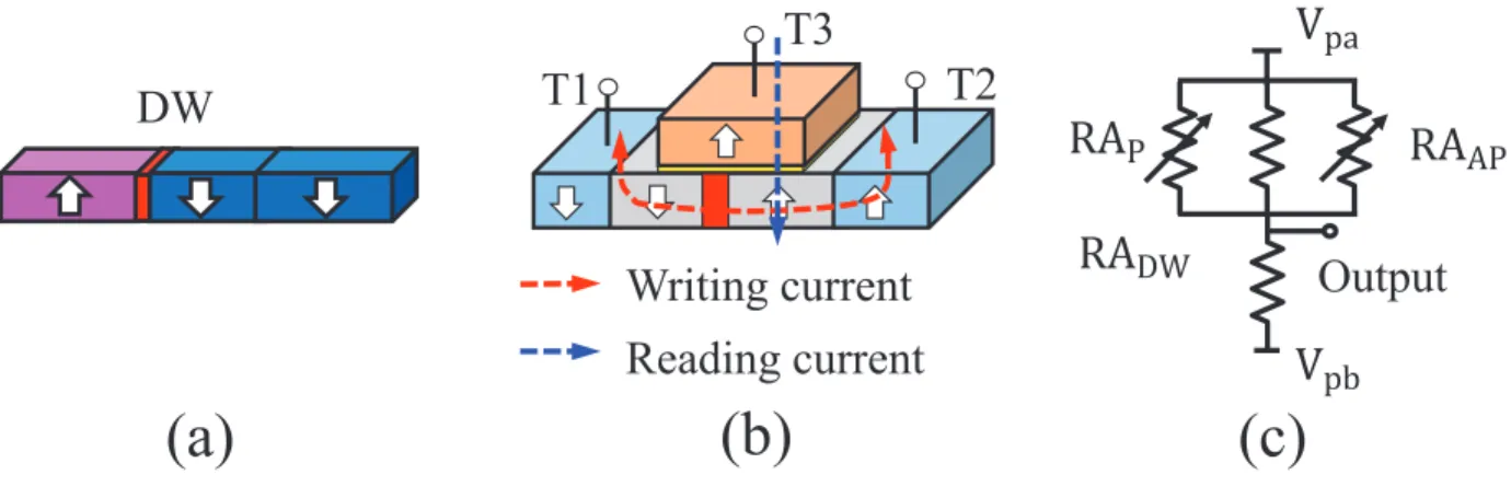
Domain Wall Device
The basic concept of the DW-motion device is that the stored information is associated with the DW position in a magnetic wire. As shown in Figure. 4.5(a), through controlling the position of the domain wall (DW), a current-induced magnetic Domain Wall (DW) motion device with a three-terminal structure can potentially enable interesting memory and logic functions. Both ends of the magnetic wire have their magnetization fixed in the anti-parallel direction relative to each other. The bidirectional current applied into the wire drags the DW back and forth, thus switching the stored information. As such, many recent studies have explored to implement novel integrated circuits with DWM devices, although mainly focused on Boolean-based logic circuits and used DWM devices as high-performance logic switches. For example, the DW motion depicted in
such as static random access memories (SRAMs), which are now facing the scaling limit.
T1
T2
T3
Writing current
Reading current
DW
Output
(a)
(b)
(c)
Figure 2.3: Schematic illustration of domain wall motion device. (a) Simplistic conceptual view. (b) More realistic Three-terminal DWM cell structure. (b) Equivalent circuital view.
Furthermore, since the DW-motion devices, like other spintronic devices, require no power supply to retain information and can be integrated in the back-end-of-line process, their implementation into integrated circuits with logic-in-memory architecture and power gating techniques allows a drastic reduction of data transfer delay and power consumption originating from charge-discharge in the interconnection and leakage current in standby mode, which are also urgent issues concern-ing recent electronics development. More practically, as shown in Figure. 4.5(b), a MTJ device is laid on the top of DW with a fixed polarity magnetic used to read the resistance. The moving of domain wall is affected by magnitude, direction and duration of injection current. The DW device has two terminals (T1, T2) separated by non-magnetic region called domain wall (DW) D2, shown
in Fig. 4.5(b). The thin nano-magnetic domain with size of 3×20×100nm3 is connecting two
anti-parallel nano-magnetic domain terminals T1 and T2. Usually, the terminal T1 is receiving input signal, wheras, terminal T2 is connected to ground. When the current is injecting in terminal T1, the spin polarity of domain D1 is written parallel to T1. Therefore, the domain wall can move through magnetic nano strip by the current injection, which leads to switching of the spin polarity in DW strip at specific location [36, 43, 38]. In Fig. 4.5 (a), the D2 is indicating domain wall area
and moving to right by spin polarized electron from T1. 0.0 ns 0.1 ns 0.2 ns 0.3 ns 0.4 ns 0.5 ns
(a)
(b)
(c)
Figure 2.4: (a) Simulation of domain wall moving by current injection in terminal T1, the do-main wall is moving to right by the spin polarized electrons. (b) Compact model presents good agreement with micromagnetic simulation for DW motion speed V as a function of current density
jp[117]. (c). A non-zero current inject to DW motion and obtains results in a hysteresis in the DW
switching characteristics [35, 64].
To illustrate and validate such behavior, we have conducted a domain wall moving simulation
with the standard Mumax3 software. Our obtained results, presented in Figure. 2.4(a), clearly
show the domain wall moving with different velocity by injecting different magnitudes of current
(1.5×10¹³A/m2 ) into the terminal T1. This simulation utilizes the device parameters: damping
coefficientα = 0.02, uniaxial anisotropy constantKu= 5.9×10⁵J/m3, saturation magnetization
Ms = 6×10⁵A/m, exchange stiffnessAex = 1×10¹¹, and polarizationP = 1[43]. The terminal
T3 is used to read the position of domain wall according to MTJ resistant. The resistant model
of MTJ is based on supplied voltage, tunnelling oxide thickness(tox), and angle of magnetization
between free layer and pinned layer. The resistant model of the proposed domain wall device
is described in [36, 40] with R = B·xA+C, where A = RAAP · RAP ·RADW, B = (RAAP −
RAP)RADW · W, and C = RAP · RADW · W · L + (RAAP · RAP − 0.5RAP · RADW −
0.5RAAP ·RADW)W ·LDW. According to these modelling equations, given the length of free
rational function of DW positions (0 < x <100nm). Finally, Figure. 2.4(c) exhibits a hysteresis phenomenon found in the DW switching characteristics. The Figure. 2.4 (c) shows the critical
current simulation for DW motion speedV as a function of current densityj.
Ferromagnetic Spin Orbit Torque Device
In Fig. 2.5, the Spin Hall Effect (SHE) assists domain wall device is shown. Comparing with the regular domain device, the SHE domain wall exerts spin orbit torque (SOT) to replace Ferro-Magnet (FM) and receive a charge current through a Heavy Metal (HM) underlayer. Recently, more papers [30, 79, 31, 91, 92] focus on research of current flowing through HM in FM-HM heterostructure, because it becomes a promising mechanism to achieve deterministic domain wall displacement. The Fig. 2.5 shows physical phenomena for domain wall motion in magnetic het-erostructures with Perpendicular Magnetic Anisotropy (PMA). The writing current is in-plane flowing through a heavy metal underlayer. The dynamic magnetization of proposed system is based on regular FM magnetization dynamics model which is described by solving Landau-Lifshitz-Gilbert (LLG) equation with additional information of Spin Orbit Torque (SOT) generated by spin hall effect at the FM-HM interface [79, 99].
d( ˆm)
dt =−γ( ˆm×Hef f) +α( ˆm× d( ˆm)
dt ) +β( ˆm×mˆP ×mˆ) (2.1)
wheremˆ is the unit vector of FM magnetization at each grid point of simulation tools,γ = 2µBµ0
}
is the gyromagnetic ratio of the electron, β = }θJ
2µ0etMs (} is Plancks constant, J is input charge
current density,θis spin hall angle,µ0is the permeability of vacuum,eis the electronic charge, t is
FL thickness andMsis saturation magnetization)αis Gilbert’s damping ratio,Heff is the effective
x
y
z
ୗୌ ୗୌUp DW
Down DW
x
y
z
Figure 2.5: The physical phenomena of SHE assisted domain wall device. The domain wall
is moving in PMA nanowires according to flow of in-plane injection current through HM layer. The SOT coupling is generated and makes stabilization of chiral Neel domain wall through DMI. According to this model, a transverse spin current is generated by in-plane injection current. The top and down view is shown in Fig. 2.5.
The effective magnetic field Heff is including the field due to Dzyaloshinskii-Moriya (DMI) [79]
by HDM I =− 2D µ0Ms [∂mz ∂x xˆ+ ∂mz ∂y yˆ−( ∂mx ∂x + ∂my ∂y )z] (2.2)
where D is the effective DMI constant and determines the strength of the DMI field in multilayer structure. The different sign of D gives different direction of chirality, positive sign implies right hand chirality and negative sign implies left hand chirality. The boundary condition is given at the edges,
∂mˆ
∂nˆ =
D
2Amˆ ×(ˆn×zˆ) (2.3)
where A is the exchange correlation constant andnˆis the unit vector based on surface of the FM.
The estimated current density is based on an assumption of current is mainly passing through the FM-HM layers [79].
FPGA architecture is proposed. The Fig. 2.6 (a) shows spin obit torque neuron with three terminals based on the magnetic DW strip. The device has three magnetic domains d1, d2 and d3 associated with a magnetic tunnel junction (MTJ) with fixed magnetization on the top. The free domain d2 has free spin polarity which can be written in parallel or anti-parallel to the two fixed magnetic domain d1 and d3 through different direction of applied current at heavy metal layer. Therefore, the spin polarity at free domain d2 can sense direction (spin polarity is up if current is injecting to d1 and spin polarity is down if the current is going out from d1 and amplitude (high current amplitude pushes d2 moving with large distance, otherwise moving with small distance). The minimum altitude of injected current has requirement to flip the state of domain wall d2. This requirement phenomenon is called domain wall hysteresis, shown in Fig. 2.6 (c). The value of minimum requirement of injected current depends on critical current density for magnetic domain motion passing through free magnetic domain d2. Thus, with help of SHE, the current density of
approximatelyv 107A/cm2 can produce more than200m/sDW velocity, which is twice faster
than regular DW structure with60m/sDW velocity. The effective magnetic field of SHE assists
architecture can be expressed as, HSHE = K(σ×m), where σ is a current dependent vector by
σ =j ×z, where j is the current vector and z is the direction perpendicular to the magnetization
plane, m denotes the magnetization of magnetic domains. Notably, sinceσ is a vector, it can be
in-plane or out of plane two directions. K is defined as quality of material parameter, which is
proportional to the effectiveness of the spin hall angle θH. Therefore, a given 100 nm long free
layer with cross section area of20×2nm2 can be passed through the whole length distance with
less than 10µA in 0.5ns, shown in Fig. 2.6 (b). The non-zero current threshold of DW device
is resulted in a small hysteresis in the spin neuron physical characteristics, shown in Fig. 2.6 (c). There is research trends to reduce the threshold hysteresis to make the step response of DW device.
In order to simulate the SHE assist domain wall device, the bottom-up simulation is simulated in Fig. 2.7. The simulation model considers device physics of the SOT in FM. The device
parame-ters are obtained from previous experiments of magnetometricTa(3nm),Pt(3nm),CoFe(0.6nm),
MgO(1.8nm), andTa(2nm)nano device [30, 79], shown in Table. 2.1.
୰ୣୟୢ
୧୬
GND HM-layer
Domain wall Free Domain
݀ଵ ݀ଶ ݀ଷ
MTJ
(a) (b) (c)
Figure 2.6: Schematic spin neuron device with spin torque layer. (a) Three-terminal DWM cell structure. (b) DW speed with and without SHE assist. (c) DW switch characteristics. The
hystere-sis characteristics depends on critical currentIcof DW moving.
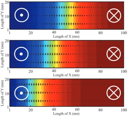
The simulation results are shown in Fig. 2.7 by usingMumax3simulation interface, a GPU based
micro-magnetic simulation tool [105]. The results show the DW DMI stabilized motion in the device according to injected current apply on HM with 0.3ns duration. According to the speed
plot in Fig.2.6 (b), given free layer with size of120nm×20nm, the injected current of25µAwill
displace the domain wall with 30nm in a duration of 0.3nm.
The variation of the device is also considered in many research papers [35, 41, 116, 74]. The resistance of the device depends upon the domain wall position, which is described through Non-Equilibrium Green’s function (NEGF) transportation framework. This framework is calibrated with experimental results and presented in [92, 41, 116, 35]. In this case, the regular NEGF trans-portation framework is modified due to parallel connection of three domains, because FM with domain wall separates two fixed oppositely polarized magnetized domains. These three domains are considered parallel, anti-parallel and perpendicular DW to the pinned layer magnetization. Fur-thermore, the resistance range of the device is also varied by physical characteristics, such as oxide
40 60 Length of X (nm) Leng th of Y ( n m ) 1 20 80 100 20 10 1 40 60 Length of X (nm) Leng th of Y ( n m ) 1 20 80 100 20 10 1 40 60 Length of X (nm) Leng th of Y ( n m ) 1 20 80 100 20 10 1
Figure 2.7: Mumax3 simulation of DW motion according to injected current of 25µA flowing
through the HM layer in 0.3ns. The given FM layer is 100nm in length with ferromagnet thickness 0.6nm.
Table 2.1: Device parameter used in simulation
Symbol Description Value
α Gilbert damping coefficient 0.3
Ku2 Perpendicular magnetic 0.48×10⁶J/m3
anisotropy constant
D Effective DMI constant −1.2×10⁻³J/m2 -torque anisotropy constant
Ms Saturation magnetization 700KA/m
ρ Resistivity of Pt 200Ω/nm
A Exchanges correlation constant 1.1×10⁻¹¹J/m
θ Spin hall angle 0.07
DW width 7.6nm
FM thickness 0.6nm
Heavy metal thickness 3nm
The variation of device resistance∆Ris a summation of variation of device resistance due to oxide
thicknessRtMgO and relative angleθ, which is between magnetization of FM and the pinned layer.
The equation of variation of device resistance∆Ris shown by following equations,
RtM gO ∝(e a0tM gO+b0 + c X m=1 ((−1)m−1Vread2meamtM gO+bm)−d (2.4) R(θ) = (( 1 RP )(cos(θ 2)) 2 + 1 RAP (sin(θ 2)) 2 )−1 (2.5)
where RP and RAP represents resistance at parallel (θ = 0) and anti-parallel (θ = π) state
respectively. The report of calibrating results of experimental data provides fitting parameters
CHAPTER 3: ULTRA-ROBUST NULL CONVENTION LOGIC CIRCUIT
WITH EMERGING DOMAIN WALL DEVICES
Introduction
Delay-insensitive asynchronous circuit possesses many attractive properties, such as low PVT de-vice’s susceptibility, high energy efficiency, high robustness, great module reusability due to its clockless nature, and the much-coveted correct-by-construction property, i.e., timing analysis is not required for its correct operation [7]. Among the many architectural variations of asynchronous circuits, NULL Convention Logic (NCL) is one of the most promising candidates. In fact, many prior studies, including real chip fabrications, have shown that NCL can be effectively designed and implemented with standard-cell based methodology [71, 56, 86].
Unfortunately, NCL circuits have some notable shortcomings, despite many significant advantages.
First, the correct operation of a NCL circuit critically depends on the use of hysteresis, which
requires the support of complicated control mechanism. Second, its use of dual-rail logic signalling based on 1-hot delay-insensitive code needs two wires per bit in NCL, thus approximately doubling its transistor usage relative to traditional CMOS circuits. Finally, the NCL circuit design is largely incompatible with the existing commercial EDA tools. As a result, fewer people are trained in this style compared to synchronous design.
Clearly, given its high hardware overhead, NCL is justifiably hard to adopt without innovations in circuit design. Fortunately, emerging spintronic device’s technology may offer at least two precious opportunities to revive the NCL circuit design.
hys-teresis, which is significantly expensive to implement with conventional CMOS circuits. In-terestingly, some emerging spintronic-based devices naturally exhibit certain physical prop-erty similar to the hysteresis in nature. Therefore, it is quite plausible to devise innovative circuit design to natively exploit these physics behavior without complicated control mech-anism.
• Spintronic devices, such as magnetic tunnel junctions (MTJ’s), spin-valves, and domain-wall
magnets (DWM), use a spin transfer torque, instead of a charge, as the medium of
informa-tion processing, therefore offering not only ultra-low critical current (e.g.,≤100µA at 65
nm), simple switching scheme, and ultra-fast-speed, but also many fascinating probabilistic-related physical properties. All these can potentially enable new NCL design methodologies in order to circumvent the reliability issues caused by the large device variations widely found in spintronic devices.
In this paper, we propose a new asynchronous NCL circuit topology based on magnetic domain wall logic. Our major contributions include:
1. In conventional CMOS-based circuit design, complicated and costly control modules have to be added in order to support the hysteresis critically needed for the correct NCL operations. In this study, we instead exploit the inherent hysteresis switching property possessed by the domain-wall-motion devices. This significantly reduces the circuit design complexity of our spintronic-based NCL circuits.
2. Leveraging emerging device technology for high performance, even for NCL circuit de-sign, is not a new idea. However, most existing studies focus on using spintronic devices as high-performance switching devices, therefore following almost identical circuit design
the correct operation of our spintronic based NCL circuits only requires the device param-eters to be in a predetermined range, thus being ultra-tolerant to the high spintronic device variations.
NCL Concept and Circuit Design
(a) A z B C B C C A B B C C A B A B C Hold0 Reset Hold1 Set !"#$ NCL Logic %"&' Reg ("&' ! ! !"&' )"&' ! NCL Logic %" Reg (" ! ! !" )" ! NCL Logic %"#' Reg ("#' ! ! !"#' )"#' ! *+,-. *",-. *+, *", *+,/. *",/.
Stage 0123 Stage 01 Stage 0143
2
(b) 2 5' 2 67 2 57 2 6' 87 8' 2 2 2 ! !97 !9' !:' 1 1 ! 2 )97 )9' ):' Ki Ko (c) N bits NCL Registers Completion RegistersFigure 3.1: NCL overall scheme: input wavefronts are controlled by local handshaking and com-pletion detection signals. (a) Traditional NCL pipeline. (b) Symbol and structure of threshold gate
TH23. (c) Implementation of logic function Z = X ⊕Y. (d) Two-bit register and completion
detector.
NCL circuit typically consists of multiple stages, each of which contains at least two registers, one at the input and one at the output, and can be finely pipelined by inserting additional registers. As
shown in Figure. 3.1(a), two adjacent register stages interact through their request and
acknowl-edge signals,Ki and Ko, respectively. To prevent the current DATA wavefront from overwriting
the previous DATA wavefront, these two DATA wavefronts are always separated by a NULL wave-front. The acknowledge signals are combined in the Completion Detection circuitry to produce the request signal(s) to the previous register stage, utilizing either the full-word or bit-wise completion strategy. Specifically, NCL circuit methodology exploits two core ideas, dual-rail signaling and
NULL signal propagation, to achieve delay-insensitivity. In NCL, each dual-rail signal,D,
trans-ported by two wires, (D0,D1), can assume one of three possible values, logic 0, logic 1, NULL
state, encoded as (1,0), (0,1), and (0,0), respectively. The unique Null state has special meaning
that the value ofDis not yet available. Note thatD0andD1 are mutually exclusive, such that both
rails can never be asserted simultaneously, therefore (1,1) is defined as an illegal state.
NCL commonly uses threshold gates with hysteresis for its basic circuit elements. The primitive
type of threshold gate is theTHm,n gate withninputs (1≤m ≤n), where at leastmofninputs
must be asserted before the output will become asserted. The typical gate symbol denoting a TH23 is shown in Figure. 3.1(b). Threshold gates can be composted to construct NCL combinational logic blocks, NCL registers, and completion detectors. Figure. 3.1(c) illustrates the
implemen-tation of an NCL combinational logic block Z = X ⊕Y using threshold gates. Figure. 3.1(d)
depicts the implementation of a 2-bit NCL register and a 2-bit completion detector using
thresh-old gates. Generally, the implementation of ann-bit NCL register needs2n TH22 gates, and the
implementation of an n-bit completion detector requires n 2-input OR (i.e., TH12) gates and a
n-input C-element (i.e., THnn). One important result in designing NCL circuits is that a set of only 27 fundamental NCL gates can implement any logic function with four or fewer variables, i.e., logically complete.
Why All Spin Torque Null Convention Logic
Among the types of NCL, the static NCL gate implementation provide a good solution with faster and more reliable operation. The conventional static NCL gate is shown in Fig. 3.3 (b). The typical static NCL gate comprised of 4 transistor networks: SET, RESET, HOLD0, HOLD1. The active and hold function is implemented in CMOS. From given TH gate functionality, the SET and HOLD1 function of NCL static gate with n inputs can be expressed as:
HOLD1 =I1+I2 +· · ·+In
Z =SET + (Z−×HOLD1)
(3.1)
where theZ− is the previous output value of static NCL gate and Z is current output value. The
given the RESET function of NCL static gate with n inputs can be expressed as:
Z0 =RESET + (Z−0 ×HOLD0) (3.2)
where the Z0 is complement of Z, and Z−0 is complement of the previous output value of static
NCL gate. In Fig. 3.1 (b), the TH23 static NCL gate is given. The function of four CMOS networks is given by: SET =AB HOLD1 = A+B RESET =A0B0 HOLD0 = A0 +B0 (3.3)
However, this delay insensitive NCL gate needs the extra transistors to build HOLD0 and HOLD1 that makes the circuit area inefficient. The hardware cost of NCL circuit is usually approximately
1.5 to 2 times larger than conventional synchronous CMOS circuit. For example, in paper of [119], a number of four stage pipeline 32-bits IEEE single-precision floating-point co-processors are im-plemented both in synchronous CMOS circuit and asynchronous NCL circuit. The given designs are using the 1.2V IBM 8RF-LM 130nm CMOS process transistor, which is used to performing addition, subtraction, and multiplication. The synchronous CMOS circuit consumes 104571 tran-sistors which is around 1.5 times less than asynchronous NCL circuit consumption, which needs 158059 transistors. The domain wall device devices are considered as replacement of the CMOS transistor. They have extra-low switch energy, fast switch time, however, their device physics limits applications of spin torque devices, such as hysteresis switching behaviour. The hysteresis switch-ing behaviour describes domain wall device transfer characteristics, shown in Fig 4.5 (c). The
domain wall is moving if the input current is larger than positive critical currentIcor negative
crit-ical current−Ic. According to the physics of device, the domain wall with size of3×20×100nm3
has a critical current density J1
c,i = 5.2×10¹²A/m2 and Jc,i1 = −5.2×10¹²A/m2. Therefore,
direct mapping hysteresis requirement of NCL to hysteresis of domain wall device can avoid using of HOLD state logic function. Furthermore, the special 3D architecture of domain wall device and memristor can reduce hardware area cost dramatically. The layout of domain devices with control transistor is shown in Fig. 3.2. From the Fig. 3.2, the two bit domain wall device associated with access transistor achieves 2X higher area density compare with the single domain wall device.
d1 d2 16λ 10λ (a) d1 d2 16λ 10λ (b) BL SL BL SL
Figure 3.2: (a). Layout of single domain wall with 2 access transistor. (b). Layout of two bit domain wall with 3 access transistor.
Therefore, we realize that replacement of CMOS NCL with emerging devices though physical characteristics of emerging devices can achieve approximately 30x and 8x improvements in energy efficiency and chip layout area.
Proposed All Spin Torque Null Convention Logic
(b) ୭୳୲ ୬୳୪୪ ୮ୟ ୮ୠ ୱ୳୫ A z B C B C C A B B C C A B A B C (a) Hold0 Reset Hold1 Set
Figure 3.3: (a) TH23 static NCL gates. (b) TH23 DWL NCL gate.
In Fig. 3.3, the proposed all spin torque convention logic architecture is presented. It is obviously to see that large numbers of the transistor are used to keep delay-insensitive performance in con-ventional static NCL gate, shown in Fig. 3.3. On the contrast, in Fig. 3.3 (b), the DWL NCL gate only takes several components, whose size are smaller than a single transistor. So that, our proposed domain DWL NCL gate which is employing domain wall device with hysteresis char-acter to achieve delay intensive performance has small area than the conventional method. In our method, domain wall NCL gate employs memristors whose conductance can be precisely modu-lated by charge or flux through it can be used to implement DWL NCL. The weighted current can
current is obtained through connecting in parallel of input based on Kirchhoff’s Current Law with I-V resistor, which is implemented by domain wall device. The Fig. 5.2 (a) shows architecture of
proposed DWL NCL gate. The inputs binary are represented byV1,· · ·VnwithVddis 1 and GND
is 0, receptively. The sum of the input current depends on the number of inputs is equal to 1. So that, the larger number of input is 1, the larger sum of the input current is obtained to inject to domain wall logic device. The hysteresis of NCL logic can be also implemented by domain wall device through critical current and NULL module memristor.
In Fig. 5.2 (c), the waveform of proposed DWL NCL is shown. In steady domain, the difference of sum of writing current and NULL current is roundly equal or less critical current, therefore, the domain wall is not moving. When sum of input current is increasing with more number of the input binary bit is 1, the difference of sum of writing current and null current is roundly more than critical current, therefore, domain wall is moving by constant velocity, shown in DATA domain.
For the sensing of DW position, we use separated read and write path for reliable issue. The
constants supplied voltage is given atVpa andVpb and needed access transistor for sensing
opera-tion. The different clock signals are also needed to control different sensing of NCL gates. These techniques are required delay element for different NCL gate layer. For example, if a TH23 gate receives output from a TH44 gate, the sensing clock of TH44 is active at 1ns delay after data arrives at TH44. The sensing clock of TH23 at 1ns delay after TH44 sensing clock. The same scheme of C-element asynchronous circuit is proposed by Zianbetov [121]. According to domain wall
posi-tion, the reference is in2.5KΩand given largest sensing margin betweenVpaandVpbisv350mV.
Therefore, we setVpa andVpb as50mV and−50mV in order to keep a good sensing margin. At
the NULL domain, the inputs are all 0, therefore, the difference of sum of writing current and null current is roundly more than resetting critical current. The domain wall is moving back to initial position and ready to receive next calculation.
Transformation From Boolean NCL to Spin Torque NCL
In the previous section, the architecture of memristor with domain wall logic is proposed to gen-erating different combination of weights and threshold from NCL boolean logic. Therefore, the transformation of NCL boolean logic to DWL NCL circuit has to be considered. The algorithm of generating different inputs memristance and NULL module memristance is proposed in Algorithm 1. With helping of Algorithm 1, The weights and threshold of boolean NCL function are mapped to DWL device associated with memrisitance and critical current value. Before we introduce the
algorithm, some default definitions and values have to be declared, which is shown in step1−8
in Algorithm 1. The given boolean NCL netlistGis input to the algorithm. The index ofi, j
indi-cates different NCL gates and different input of individual NCL gate. GivenVddis used to generate
different weighted current through memristor.Tiandwi,jare written by the function ofT hres(G)
andW eigh(G), which is used to read the logic threshold and weight of individual NCL gate from
given boolean NCL netlist. The calculated memristance of inputmi,j and NULL module Mi are
the output of Algorithm 1, which is constrained in range ofmminandmmax. The value ofmminand
mmax is obtained from memristor device, in our case, range is from100Ωto< 38000Ω. The two
domain wall device critical current densities are used to achieve hysteresis of NCL. The domain
wall device critical current density J c, i1 andJ2
c,i for each NCL gate is given by measurement of
DW device [43]. The domain wall device critical current densityJ2
c,i = 6.2×10¹²A/m2will cause
domain wall moving with20m/svelocity. On another side, current densityJ1
c,i = 5.2×10¹²A/m2
will cause domain wall moving with0m/svelocity. The critical currentI1
c,iandIc,i2 are calculated
by injection area and critical current density. In order to explain the algorithm clearly, we consider
two the boolean NCL gates TH23W2 and TH44 with function of f = A+BC, f = ABCDas
example, respectively. For boolean NCL functionf = A+BC, three inputs weights are (2,1,1)
with threshold is 2. Since the weights of each input is different with each other, therefore, the
memristance values are calculated for functionf = A+BC as follows, the sequent of memris-tance A, B, C ism1,1, m1,2, m1,3.
Case 1: Hysteresis-set 1:
The sum of input current is smaller than threshold and not making domain wall moving, therefore,
Vdd m1,2 − Vdd M1 < I 1 c,1 and Vdd m1,3 − Vdd M1 < I 1
c,1 are both true.
Case 2: Set 1:
The sum of input current is larger than threshold value make domain wall moving, therefore,
2· Vdd m1,2 − Vdd M1 > I 2 c,1 and Vdd m1,1 − Vdd M1 > I 2
c,1are both true.
Case 3: Hysteresis-set NULL:
The sum of input current is larger than negative threshold and not making domain wall moving
back, therefore, Vdd m1,2 − Vdd M1 >−I 1 c,1 , and Vdd m1,1 − Vdd M1 >−I 1
c,1 are both true.
Case 4: NULL:
The sum of input current is zero and making domain wall moving back to initial position, there-fore,−Vdd
M1 <−I
2
c,1 is true.
The possible memristance of 3 different inputs and Null module are given by equation above.
with Vdd is equal to 0.3V The memrsiatnce of input A is mi,A = 608Ω, memrsiatnce of input
B is mi,B = 1209, memrsiatnce of input C is m1,C = 1209Ω, memrsiatnce of Null module is
Mi = 1209Ω, receptively. For the TH44 gatef =ABCD, the method is similar with above, the
memrsiatnce of input A ismi,A = 2418Ω, memrsiatnce of input B ismi,B = 2418Ω, memrsiatnce
of input C is mi,C = 2418Ω, memrsiatnce of input D is mi,D = 2418Ω, memrsiatnce of Null
module isMi = 1209Ω.
The algorithm is applying to 27 typical TH gate truth tables, in order to verify results. This algo-rithm shows that the TH gate can be classified into 5 different groups according to its threshold.
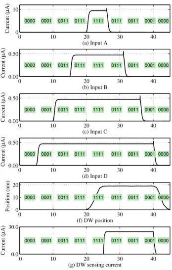
0 10 20 30 40 0 10 (a) Input A Current ( µ A) 0000 0001 0011 0111 1111 0111 0011 0001 0000 0 10 20 30 40 0.00 0.50 (b) Input B Current ( µ A) 0000 0001 0011 0111 1111 0111 0011 0001 0000 0 10 20 30 40 0.00 0.50 (c) Input C Current ( µ A) 0000 0001 0011 0111 1111 0111 0011 0001 0000 0 10 20 30 40 0.00 0.50 (d) Input D Current ( µ A) 0000 0001 0011 0111 1111 0111 0011 0001 0000 0 10 20 30 40 0 10 20 (f) DW position Position (nm) 0000 0001 0011 0111 1111 0111 0011 0001 0000 0 10 20 30 40 0.0 30.0 (g) DW sensing current Current ( µ A) 0000 0001 0011 0111 1111 0111 0011 0001 0000
Figure 3.4: Simulation of proposed TH44 gate through domain wall logic device.
According to the configuration of this DW device, current density 6.2× 10¹²A/m2 will cause
domain wall moving with 20m/s velocity, on the contract, current density 5.2×10¹²A/m2 will
cause domain wall moving with0m/s velocity. The results of mapping Algorithm1 is shown in
Table 3.1, Table 3.2, Table 3.3.
According to the results from Table 3.3, we take NCL TH44 gate for example. The DW simulation
is done by softwaremumax3with parameters, shown in Table. 3.4. When the sum of input current
Algorithm 1: Calculating Stochastic weight and threshold algorithm
Input :G-Boolean NCL netlist
Output:N-DWL NCL netlist
1 Vdd←0.3V
2 S←40nm2 // injection area of domain wall
3 Ti←Thres(G) // read threshold of each node
4 wi,j←Weigh(G) // read weight of each node
5 mmin←100Ω // set minimal memristance
6 mmax←38000Ω // set minimal memristance
7 Ic1
i ←S·5.2×10¹²A/m2 // set critical current density for DW velocity=0
8 Ic2i ←S·6.2×10¹²A/m2 // set critical current density for DW velocity=20m/s
9 fori= 1 :Ndo
10 ifwi,j=wi,1,· · ·,=wi,nithen
11 minimize(mi,j=1:n) // find the minimal memritance of input j=1:n
12 subject to: 13 Ti·mVdd i,j− Vdd Mi > Ic 2 i // set 1
14 (Ti−wi,j)·mVddi,j−VMddi < Ic1i // hysteresis
15 −Vdd Mi <−Ic 2 i // null 16 Vdd mi,j − Vdd Mi >−Ic 1 i // hysteresis
17 mmin< mi,j, Mi< mmax // device constraint
18 else
19 wmin←f indmin(wi,j) // find the minimal boolean weight of input j=1:n
20 mi,j=1:n←mwmin·
wi,j
wmin // calculate memristance of each input
21 minimize(mwmin) // find the minimal memritance of input j=1:n
22 subject to: 23 Ti·mVdd wmin − Vdd Mi > Ic 2 i // set 1 24 (Ti−wmin)·mVdd wmin − Vdd Mi < Ic 1 i // hysteresis 25 −Vdd Mi <−Ic 2 i // null 26 Vdd mwmin − Vdd Mi >−Ic 1 i // hysteresis
27 mmin< mi,j, Mi< mmax // device constraint
At the time of 4 inputs are high, the sum of current is larger than critical current and move domain right to terminal T2. Therefore, the different combinations of inputs can make domain wall moving or stepping. The simulation of TH44 gate is shown in Fig. 3.4. The number of inputs is increasing sequentially to test hysteresis. Before the four inputs are all ones, the different combinations of
input are shown in Fig. 3.4, A = 0, B = 0, C = 0, D = 0, A = 0, B = 0, C = 0, D = 1,
A = 0, B = 0, C = 1, D = 1, , A = 0, B = 1, C = 1, D = 1. At those cases, domain wall is
stepped since the sum of input current and NULL module current are not larger than critical current. While the four inputs are all active, the sum of the input current and NULL module current is larger than critical current and making domain wall moving. After the domain wall moves to a specific
Table 3.1: One and two inputs mapping results of proposed Algorithm1 for 27 foundational NCL functions
NCL gate Boolean function Weight: Memristance Range(Ω)
Threshold TH12 A+B (1,1:1) mi,A,mi,B ∈[100,Mi/2]; Mi∈[100,1209] TH13 A+B+C (1,1,1:1) mi,A,mi,B,mi,C ∈[100,Mi/2]; Mi∈[100,1209] TH14 A+B+C+D (1,1,1:1) mi,A,mi,B,mi,C,mi,D ∈[100,Mi/2]; Mi∈[100,1209] TH22 AB (1,1:2) mi,A,mi,B,Mi∈[100,1209] TH23 AB+AC+BC (1,1,1:2) mi,A,mi,B,mi,C,Mi ∈[100,1209] TH23W2 A+BC (2,1,1:2) mi,A∈[100,Mi/2]; mi,B,mi,C,Mi ∈[100,1209] TH24 AB+AC+AD (1,1,1,1:2) mi,A,mi,B,mi,C ∈[100,1209] +BC+BD+CD mi,D,Mi∈[100,1209] TH24W2 A+BC (2,1,1,1:2) mi,A∈[100,Mi/2]; +BD+CD mi,B,mi,C,mi,D,Mi ∈[100,1209] TH24W22 A+B+CD (2,2,1,1:2) mi,A,mi,B ∈[100,Mi/2]; mi,C,mi,D,Mi∈[100,1209]
At those cases, the domain wall is not moving back to initial position, since an inverse current is not larger than resetting critical current, the domain wall is still stepped at its current position. At the time of all inputs are zeros, the sum of the input currents and Null module current is larger than resetting critical current, and pushing domain wall back to its original position. The simulation is shown in Fig. 3.4. From the simulation, the hysteresis of NCL logic is implemented through domain wall hysteresis by using different memristance.
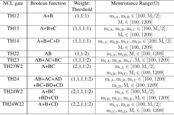
Among the 27 NCL gates, there are 3 special NCL function (TH24comp, THand0, THxor0), which are not threshold gate [87]. In order to implement these NCL gates, we decompose them to sub NCL gate. The Fig. 3.5 (a) (b) (c) show architecture of spin-torque-transfer DW device based NCL (TH24comp, THand0, THxor0) gate.
Table 3.2: Two and three inputs mapping results of proposed Algorithm1 for 27 foundational NCL functions
NCL gate Boolean function Weight: Memristance Range(Ω)
Threshold TH33 ABC (1,1,1:3) mi,A,mi,B,mi,C ∈[100,(2/3)·Mi]; Mi∈[100,1209] TH33W2 AB+AC (2,1,1:3) mi,A∈[100,(3/4)·Mi]; mi,B,mi,C ∈[100,(3/2)·Mi]; Mi∈[100,1209] TH34 ABC+ABD (1,1,1,1:3) mi,A,mi,B,mi,C,mi,D ∈[100,(3/2)·Mi]; +ACD+BCD Mi∈[100,1209] TH34W2 AB+AC (2,1,1,1:3) mi,A∈[100,(3/4)·Mi]; +AD+BCD mi,B,mi,C,mi,D∈[100,(3/2)·Mi] +AD+BCD Mi∈[100,1209] TH34W3 A+BCD (3,1,1,1:3) mi,A ∈[100,Mi/2] mi,B,mi,C,mi,D∈[100,(3/2)·Mi] Mi∈[100,1209] TH34W22 AB+AC (2,2,1,1:3) mi,A,mi,B ∈[100,(2/3)·Mi] +AD+BC+BD mi,C,mi,D ∈[100,(3/2)·Mi] ; Mi∈[100,1209] TH34W32 A+BC+BD (3,2,1,1:3) mi,A∈[100,Mi/2]; mi,B∈[100,(2/3)·Mi] mi,C,mi,D ∈[100,(3/2)·Mi] Mi∈[100,1209]
The proposed architecture is based on the decomposition of NCL function set. For example, the NCL gate THxor0 can be decomposed to two layers architecture that consists of 2 TH22 gates and 1 TH21 gate, shown in Fig. 3.5 (d). The NCL gate THand0 can be decomposed to two layers architecture that consists of 3 TH22 gates and 1 TH21 gate, shown in Fig. 3.5 (e). The NCL gate TH24comp can be decomposed to two layers architecture that consists of 2 TH21 gates and 1 TH22 gate, shown in shown in Fig. 3.5 (f). The simulations of different proposed NCL gate are simulated in Fig. 3.5 (g) (h) (i), respectively. The active input number is increasing sequentially. For THxor0 gate, at the time of inputs of C and D are active, the DW device for input C and D is
Table 3.3: Four and five inputs mapping results of proposed Algorithm1 for 27 foundational NCL functions
NCL gate Boolean function Weight: Memristance Range(Ω)
Threshold TH44 ABCD (1,1,1,1:4) mi,A,mi,B,mi,C,mi,D =∈[100,2·Mi] Mi ∈[100,1209] TH44W2 ABC+ABD (2,1,1,1:4) mi,A,Mi ∈[100,1209] +ACD mi,B,mi,C,mi,D∈[100,2·Mi] TH44W3 AB+AC+AD (3,1,1,1,4) mi,A∈[100,(2/3)·Mi] mi,B,mi,C,mi,D∈[100,2·Mi] Mi ∈[100,1209] TH44W22 AB+ACD (2,2,1,1:4) mi,A,mi,B,Mi∈[100,1209] +BCD mi,C,mi,D ∈[100,2·Mi] TH44W322 AB+AC (3,2,2,1:4) mi,A∈[100,(2/3)·Mi] +AD+BC mi,B,mi,C,Mi∈[100,1209] mi,D∈[100,2·Mi] TH54W22 ABC+ABD (2,2,1,1:5) mi,A,mi,B ∈[100,(5/4)·Mi] mi,C,mi,D∈[100,(5/2)·Mi] Mi ∈[100,1209] TH54W32 AB+ACD (3,2,1,1:5) mi,A∈[100,(5/4)·Mi] mi,B ∈[100,(5/4)·Mi] mi,C,mi,D∈[100,(5/2)·Mi] Mi ∈[100,1209] TH54W322 AB+AC (3,2,2,1:5) mi,A∈[100,(5/6)·Mi]; +BCD mi,B,mi,C ∈[100,(5/4)·Mi] mi,D∈[100,(5/2)·Mi] Mi ∈[100,1209]
Sequentially, the sum of injection current from AB and CD to DW device on the second layer is higher than second DW critical current. Therefore, second layer DW device is shifting and
producing a high voltage output. Since sensing currents of both DW device are set to 30µA to
keep a good amount of sensing margin, the current inject to the second layer DW device is very small to achieve TH gate operation with hysteresis.
2 1 2 A B C D F F=AB+CD 1 2 1 A B C D F F=AC+BC+AD+BD 2 1 2 A B C D F F=AB+BC+AD 2
(a)
(b)
(c)
(g)
(e)
(f)
(d)
(h)
(i)
Figure 3.5: (a) CMOS NCL THXOR gate (b) CMOS NCL THand0 gate (c) CMOS NCL
TH24comp gate (d) Spin-torque-transfer DW device based NCL THXOR gate architecture (e) Spin-torque-transfer DW device based NCL THand0 gate architecture (f) Spin-torque-transfer DW device based NCL TH24comp gate architecture (g) Simulation of Spin-torque-transfer DW device based NCL THXOR gate architecture (h) Simulation of Spin-torque-transfer DW device based NCL THand0 gate architecture (i) Simulation of Spin-torque-transfer DW device based NCL TH24comp gate architecture
Table 3.4: Device simulation used in simulation of TH44 gate
Symbol Description Value
α damping coefficient 0.02
Ku uniaxial anisotropy constant 0.59×10⁶J/m3 Xi Non-adiabaticity of spin-transfer 0.2
-torque anisotropy constant
M s saturation magnetization 6×10⁵A/m
P polarization 0.6
Aex exchanges stiffness 1.1×10¹¹J/m
Proposed Asynchronous Circuit Design Through Magnetic Domain Wall NCL Gate
(a)
(b)
Figure 3.6: (a) Dual rail spin torque NCL architecture with reading scheme. (b) Simulation
of NPN transistor with different supplied voltage Vcc. The input current is generated from DW
sensing current and amplified through NPN transistor.
The typical asynchronous circuit is implemented by Delay Insensitive (DI) asynchronous pipeline with a dual rail 4-phase handshake protocol 3.7 (e). In Fig. 3.7 (e) , dual rail signal D has two wires,
D0 andD1. Any values from dual rail set{DAT A0, DAT A1, N U LL}can be presented through
different combinations ofD0 and D1. The DAT A0 is represented by (D0 = 1, D1 = 0), which
is corresponding to boolean logic 0, TheDAT A1 is represented by (D0 = 0, D1 = 1), which is

![Figure 3.12: IEEE single precision floating point co-processor architecture [119].](https://thumb-us.123doks.com/thumbv2/123dok_us/10227164.2926570/60.918.227.699.158.458/figure-ieee-single-precision-floating-point-processor-architecture.webp)
![Table 3.6: Comparison of different design implementation for 32 bit IEEE single-precision floating point co-processor [119].](https://thumb-us.123doks.com/thumbv2/123dok_us/10227164.2926570/61.918.108.822.157.382/table-comparison-different-design-implementation-precision-floating-processor.webp)
