Full Length Article
An efficient ternary serial adder based on carbon nanotube FETs
Mohammad Hossein Moaiyeri
*
, Molood Nasiri, Nooshin Khastoo
Nanotechnology and Quantum Computing Lab, Shahid Beheshti University, Tehran, Iran
A R T I C L E I N F O Article history:
Received 8 May 2015 Received in revised form 10 July 2015
Accepted 28 July 2015
Available online 2 September 2015 Keywords:
Carbon nanotube FET Multiple-valued logic Ternary logic Serial adder
A B S T R A C T
This paper presents an efficient ternary serial adder for nanotechnology employing negative, positive and standard ternary logics. Multiple-valued logic results in chips with more density, less complexity and high-bandwidth data transfer. The unique properties of CNTFETs such as the capability of adapting the desired threshold voltage by changing the diameters of the nanotubes and same carrier mobility for the n-type and p-type devices play an important role in designing this circuit. The proposed design method considerably reduces the number of required devices of a ternary serial adder. In addition, the results of the simulations conducted using HSPICE with the Stanford comprehensive 32 nm CNTFET model, dem-onstrate improvements in terms of speed and power-delay product as compared to the cutting-edge CNTFET-based ternary designs.
Copyright © 2015, The Authors. Production and hosting by Elsevier B.V. on behalf of Karabuk University. This is an open access article under the CC BY-NC-ND license (http://creativecommons.org/ licenses/by-nc-nd/4.0/).
1. Introduction
Complementary metal oxide semiconductor (CMOS) is the main technology of the past decades that provides the satisfactory di-mension scaling in order to achieve energy-efficient and
high-density very large scale integration (VLSI) circuits[1]. However,
scaling down the feature size of CMOS devices in nanometer regime results in challenges such as short-channel effects and reduced gate control. These problems can obstruct the consecutive dimension scaling of the CMOS technology and consequently reduces its ap-propriateness for the prospect speed, energy-efficient
high-density applications[2]. Basic limitations of CMOS technology and
expectations of Moore’s law have prompted scientists to find a con-venient alternative for this apparatus.
In order to overcome the aforementioned limitations, research-ers try to develop other nanotechnologies such as silicon nanowire transistors, single electron transistor (SET), quantum-dot cellular au-tomata (QCA) and carbon nanotube field effect transistors (CNTFET)
[1–4]. Due to the remarkable properties of CNTFET, it seems to be a promising successor for CMOS among the various introduced al-ternatives. The similarities between the substructure of the conventional MOSFET and CNTFET make CNTFET a more feasible nanodevice for use in the structures designed based on CMOS without making any major changes. Moreover, because of the unique one-dimensional band structure of CNTFET, which suppresses back-scattering and causes near-ballistic operation, CNTFET represents
a very high-speed operation[5]. Considering higher performance,
higher carrier velocity, higher transconductance and lower power consumption, CNTFET significantly illustrates greater perfor-mance than conventional CMOS transistors.
On the other hand, unlike the binary logic, there are more than two authorized logic levels in MVL systems so logical and arith-metic operations can be performed on more than two logic values. As a result, in MVL many logical and arithmetic operations could be executed with higher speed and smaller number of
computa-tion stages[5]. In addition, the most suitable method for designing
voltage-mode MVL circuits is multiple-threshold (multi-Vt) design
method and the desired threshold voltage can be achieved by setting
the diameters of the nanotubes in CNTFET devices[4–7].
Consid-ering the fact that in a typical binary VLSI chip almost 70% of the chip area is dedicated to the interconnects, 20% to the insulation, and just 10% to the device itself, it is not irrational to claim that di-minished space on VLSI chips restricts the performance of binary
logic[8]. Multiple-value logic can lead to increased data
process-ing capability per unit area, reduced number of interconnections, as well as reduced number of active devices inside a chip, as com-pared to the binary logic. MVL modules have been applied to binary logic ICs to improve the performance of CMOS technologies. For in-stance, employing an efficient MVL implementation for a signed 32-bits multiplier compared to its fastest binary equivalent can lessen
chip area and power consumption more than 50%[6]. Moreover, by
utilizing multiple-valued logic, serial and serial–parallel
arithmet-ic operations can be carried out faster[5].
Considering different MVL systems, using radixe(e=2.718. . .)
results in the most efficient design of the digital systems. Never-theless, because of the restriction on hardware implementation, designers are restricted to use natural numbers as the bases for
* Corresponding author. Tel.:+98 2129904109, fax:+98 2122431804. E-mail address:[email protected](M.H. Moaiyeri).
Peer review under responsibility of Karabuk University. http://dx.doi.org/10.1016/j.jestch.2015.07.015
2215-0986/Copyright © 2015, The Authors. Production and hosting by Elsevier B.V. on behalf of Karabuk University. This is an open access article under the CC BY-NC-ND license (http://creativecommons.org/licenses/by-nc-nd/4.0/).
Contents lists available atScienceDirect
Engineering Science and Technology,
an International Journal
j o u r n a l h o m e p a g e : h t t p : / / w w w. e l s e v i e r. c o m / l o c a t e / j e s t c h
Press: Karabuk University, Press Unit ISSN (Printed) : 1302-0056 ISSN (Online) : 2215-0986 ISSN (E-Mail) : 1308-2043
Available online at www.sciencedirect.com ScienceDirect
calculations. As a result, the most efficient MVL system, which results
in lower cost and complexity than binary, is the ternary logic[9].
Full Adder is definitely the most important circuit among the various processing elements used in a microprocessor. Perfor-mance improvement of signal processors mainly depends on the development of adder circuits. Therefore designing an efficient CNTFET-based quaternary full adder cell supporting all the possi-ble logic values for the near future non-silicon non-binary integrated circuits and systems can be more of an interest.
Full Adder is definitely the most important arithmetic module used in a microprocessor. Hence, performance improvement of signal processors mainly depends on the development of efficient adder circuits. In addition, serial addition can be better for low-energy ap-plications and leads to a considerable hardware efficiency.
According to the aforementioned discussions, designing an ef-ficient CNTFET-based ternary serial adder for the near future non-silicon non-binary integrated circuits and systems can be more of an interest. In this paper, an efficient ternary serial adder is pro-posed using CNTFET.
The rest of the paper is organized as follows:Sections 2and3
briefly review the CNTFET nanodevice and ternary logic,
respec-tively. The proposed design is described inSection 4.Section 5
includes the simulation results and finallySection 6concludes the
paper.
2. A brief overview of the CNTFET nanodevice
Carbon Nanotube (CNT) was discovered in 1991 by S. Iijima. CNT is a nano-scale tube which is made up of rolled sheet of graphene. CNT falls into two categories, multi-wall (MWCNT) and single-wall (SWCNT). A MWCNT is composed of more than one cylinder while a SWCNT is a single cylinder. A SWCNT could be a semicon-ductor or a consemicon-ductor, depending on its chirality vector. The chirality vector is the wrapping vector that the graphene sheet is
consid-ered to be rolled up along and is defined by (n1, n2) indices. They
determine the arrangement angle of the carbon atoms along the
nanotube. Ifn1−n2≠3k(k∈Z), the SWCNT is a semiconductor and
otherwise it is metallic. Semiconducting SWCNTs can be used as the
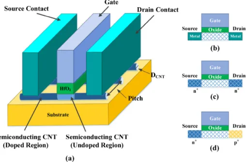
channel of the CNTFET device[10–12].Fig. 1aillustrates a general
structure of a CNTFET device.
Unlike the silicon MOSFET, p-type and n-type CNTFETs have the
same carrier mobility (μn=μp) and hence the same drive current
capability[10]. This unique characteristic of the CNTFET device is
very significant for simplifying the design and transistor sizing pro-cedures of complex CNTFET-based circuits.
Another great advantage of the CNTFET nanodevice in compar-ison with the nanoscale MOSFET is its I–V characteristics which are similar to well-tempered classic MOSFET devices. In addition, similar to a MOSFET, a CNTFET also has a threshold voltage, which is the voltage required for turning on the device via the gate. Adapting threshold voltage of a CNTFET just by changing the diameter of its CNTs makes it more flexible than MOSFET for designing digital
cir-cuits and also very appropriate for designing multi-Vtcircuits. The
threshold voltage of a CNTFET is approximately considered as the
half bandgap and can be calculated by equation(1) [10].
V E e aV eD D nm th g CNT CNT 2 3 3 0 43 =
( )
π . (1)wherea(≃0.249 nm) is the carbon to carbon atomic distance,Vπ
(≃3.033 eV) is the carbon π–π bond energy in the tight bonding
model,eis the unit electron charge andDCNTis the diameter of CNTs,
which is calculated by equation(2) [10].
DCNT=a n +n +n n n +n +n n 1 2 2 2 1 2 12 22 1 2 0 0783
π
. (2)It can be inferred from equations(1)and(2)that by changing
the diameter and the wrapping vector of a CNT, which is defined
by its chirality indices (n1, n2), the bandgap of CNT and threshold
voltage of CNTFET can be modified.
It is worth pointing out that various useful and operational so-lutions have already been presented in the literature for growing CNTs with a defined chirality and implementing the desired
thresh-old voltage for multi-tube CNTFETs[13–15].
Three distinct forms of CNTFET devices have been already in-troduced in the literature. Schottky Barrier (SB) CNTFET is the first
one (Fig. 1b), a tunneling device operating in the rules of direct
tun-neling through a SB at the source–channel junction. Due to its fabrication, which uses direct contact between the semiconductor CNT and the metal, it has a SB at the CNT–metal junction that causes
Fig. 1.CNTFET. (a) Detail structure of MOSFET-like CNTFET. (b-d) Three different types of CNTFET. 272 M.H. Moaiyeri et al./Engineering Science and Technology, an International Journal 19 (2016) 271–278
limitation for the transconductance of the CNTFET in the ON state and degrades of current delivery capability in it. In an effort to fab-ricate CNTFETs which would operate like normal MOSFETs but with superior performance, heavily-doped source and drain CNT regions have been generated and the field-effect and unipolar characteris-tics have been reached. The absence of SB in source–channel junction and consequently higher ON current is determined as the main merit
of this kind of CNTFET, named MOSFET-like CNTFET (Fig. 1c).
Ac-cording to the mentioned facts, the MOSFET-like CNTFETs are better suited for ultra-high-speed digital applications. Another kind of CNTFET, called the band-to-band tunneling CNTFET (T-CNTFET) (Fig. 1d), has low ON currents but super cut-off characteristics and
is very suitable for subthreshold applications[16,17].
The above-mentioned pros and cons of distinctive types of CNTFETs and remarkable similarities between MOSFET-like CNTFETs and MOSFETs in terms of the operation and intrinsic attributes, have made them the best option in this paper for designing the pro-posed circuits.
3. A review of the ternary logic
Ternary logic as one of the MVL families that considers three allowed significant logic values represented with “0”, “1” and “2”
symbols which are equivalent to voltages around 0 V, ½ VDD, and
VDDvoltage values. Three different forms, negative, standard and
pos-itive logics, can be defined in ternary logic. The basic logic operators in ternary logic are NOT, minimum and maximum. A ternary
in-verter, with the inputaandNoti(a)output, operates based on the
following equation: Not a i if a a if a i
( )
= = − ≠ ⎧ ⎨ ⎩ 1 2 1 (3)By choosing the logic values 0, 1 and 2 fori, a ternary inverter
can be negative ternary inverter (NTI), standard ternary inverter (STI) and positive ternary inverter (PTI), respectively.
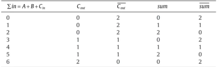
The most fundamental ternary arithmetic block is the 1-trit ternary full adder circuit. The truth table of a ternary full adder with
A, B, Cin(input carry) inputs and Sum and Cout(output carry) outputs
is shown inTable 1.
Many efforts have been made to implement the ternary logic and arithmetic operations. Using MOSFET technology, numerous types of CMOS-based MVL circuits have been proposed in the
literature [18–21]. However, they undergo many shortcomings
such as requiring ohmic resistors, employ multiple supply volt-ages, high static power dissipation and using depletion-mode MOSFETs which significantly restrict their suitability for the modern technologies.
In the recent years, advanced CNTFET-based ternary logical and arithmetic circuits have also been presented in the literature. A number of CNFET based circuits have been represented in
Refer-ence6. In spite of the advantages of utilizing CNTFET transistors,
they use large ohmic resistors that are challenging to be em-ployed on-chip and integrated with CNTFETs and also cause space wastage and of performance degradation. To overcome the above-mentioned problems, other ternary logical and arithmetic circuits
have been proposed in References3and5in which P-CNTFET active
loads have been used instead of large ohmic resistors. This tech-nique leads to a better integration, higher speed, less area overhead, in comparison with the conventional CNTFET-based ternary
cir-cuits of Reference6.
In Reference22a ternary full adder has been presented based
on two cascaded ternary half adder (THA) cells (Fig. 2a) and a carry
generator unit (Fig. 2b). The first THA adds two input operands (A
and B) and the result (H) is subsequently transferred to the second THA to generate the sum signal and is also fed to the carry
gener-ator unit. In the second THA the result of A+B (denoted as H) is
added to the input carry (C), which results in the sum signal. In ad-dition, in the carry generation unit the output carry is produced based on the full adder inputs and the H signal. This design re-quires 88 transistors and additional transistors are required to
Table 1
Truth table of a ternary full adder cell.
∑ = + +in A B Cin Cout Cout sum sum
0 0 2 0 2 1 0 2 1 1 2 0 2 2 0 3 1 1 0 2 4 1 1 1 1 5 1 1 2 0 6 2 0 0 2
generate the required complemented input signals if they are not available.
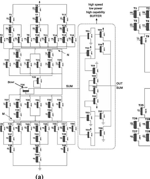
Another full adder cell consists of two parts to generate the sum
and carry signals have been presented in Reference23, which is
shown inFig. 3. Two ternary values and the carry of the previous
stage are added and then the sum and carry values are produced. This ternary full adder has two separate parts which are a sum
gen-erator circuit (Fig. 3a) and a carry generator circuit (Fig. 3b). In this
design logic “1” is produced based on resistive voltage divisions by utilizing diode connected p-type and n-type CNTFETs. This ternary full adder employs 114 transistors and additional transistors are needed to produce the required complemented input signals if they are not available.
4. The proposed CNTFET-based serial adder
One of the momentous ternary arithmetic circuits, ternary serial adder cell, is a digital circuit that can add every two arbitrary large numbers using a single full adder and a flip flop. A schematic diagram of a ternary serial adder consisting a ternary full adder and a ternary
D-flip flop is shown inFig. 4.
Since the carry-out of the full adder becomes the carry-in of the full adder on the next operation, a D-flip flop is used to save the carrier signal.
According to the truth table of ternary full adder, given inTable 2,
equation(3)is concluded[17]:
in A B Cin Cout Sum
∑ = + + =3 + (4)
Dividing both sides of it by 3 results:
in
Cout Sum
∑ = +
3 3 (5)
Using floor function with ⎣⎦ symbol which returns the integer
part of every quantity and the fact that in ternary logic0
3 1
≤Sum<
and Cout∈
{
N, 0}
, value ofCoutis defined by equation(6):Cout= ∑⎢ in
⎣⎢ 3 ⎥⎦⎥ (6)
AsCout=2-Cout, by replacingCoutwith the mentioned relation in
equation(3), Sumis calculated as follows:
Sum=
∑
in+3Cout-6 (7)The ternary full adder of Reference17, generatingSumandCout
signals based on equations(6)and(7), is utilized as the building
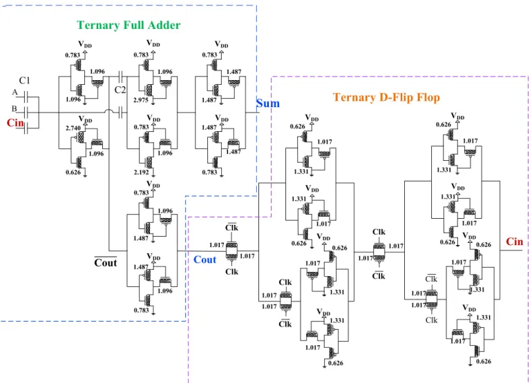
block of the proposed ternary serial adder. The schematic of the basic
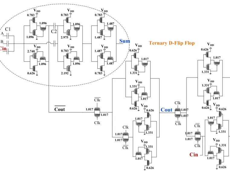
proposed design for ternary serial adder is shown inFig. 5. Both of
thesumandCoutgenerator modules in this design are made up based
on a capacitor-based scaled analog summation plus a ternary buffer
which includes two ternary inverters[3]. The ternary buffer is indeed
two cascaded ternary inverters, in which the first inverter is the threshold detector block for implementing the floor function and the second one is a standard ternary inverter that produces the signal
Coutfrom the generated Cout. It is also noteworthy that the
thresh-olds of the ternary threshold detector circuit can be adjusted by choosing proper threshold voltages for its binary CNTFET-based in-verters which is exactly equivalent to adopting proper diameters
for the channels of the CNTFETs according to equation(1). It is
note-worthy that in order to improve the performance and efficiency of the proposed serial adder, the number of required distinct diam-eters is reduced as compared to the full adder presented in Reference
17.
Another part of the proposed serial adder is a D-flip flop which includes four ternary inverters and four transmission gates and has 32 transistors. This static ternary flip-flop structure is designed based on standard ternary inverters and do not require any additional supply voltage.
Every carry-out number generated by the full adder remains in the flip flop for one clock cycle and then in the next cycle adds to the two other inputs as one of the inputs of the full adder.
Since, in the full addersumandCoutsignals are obtained from
Sum and Cout and due to existence of ternary inverters in the
D-flip flop structure, the fragment that is producing Cout fromCout
can be omitted. Then, in order to reach valid output, expected
yield should be achieved at the point which is shown inFig. 6. As
a result, in ensuing action to advance the proposed design, in
ultimate design, demonstrated inFig. 6, one of the six major modules
creating serial adder has been omitted and therefore the number of transistors has been reduced to only 55 transistors. As a result, the proposed design provides outstanding function which substan-tially reduces the number of transistors and enhances the speed and energy efficiency.
5. Simulation results and comparison
The serial adders, including the proposed circuit and the ternary serial adders based on the state-of-the-art designs of References
22and 23are simulated at 0.9 V supply voltage using Synopsys
HSPICE 2008 and the Stanford comprehensive SPICE model for
CNTFET including nonidealities at 32 nm technology [17]. This
standard model has been designed for unipolar enhancement-mode MOSFET-like CNTFET devices, in which each transistor may include one or more CNTs as its channel. This model also consid-ers a realistic, circuit-compatible CNTFET structure and includes practical device nonidealities, parasitics, Schottky-barrier effects at the contacts, inter-CNT charge screening effects, doped source– drain extension regions, scattering (nonideal near-ballistic transport), back-gate (substrate bias) effect and Source/Drain, and Gate resis-tances and capaciresis-tances. Furthermore the model embraces a complete transcapacitance network for more precise transient and dynamic performance simulations. The parameters of the CNTFET model and their values, with brief descriptions, are shown inTable 2.
The transient response of the proposed ternary serial adder is
demonstrated inFig. 7which indicates the correct operation of
the proposed design. It is worth pointing out that the output glitches, which occur only when the inputs change, will not be
Table 2
Important parameters of the CNTFET model.
Parameter Value
Physical channel length 32 nm
The mean free path in the intrinsic CNT 100 nm The length of doped CNT drain-side region 32 nm The length of doped CNT source-side region 32 nm The mean free path in p+/n+doped CNT 15 nm The distance between the centers of two adjacent CNTs withi
n the same gate
≤30 nm
Sub-lithographic pitch 4 nm
The thickness of high-k top gate dielectric 4 nm The dielectric constant of high-k top gate dielectric material
(HfO2)
16 The dielectric constant of substrate (SiO2) 4 The coupling capacitance between the channel region and the
substrate (SiO2)
40 aF/μm
The Fermi level of the doped S/D CNT 6 eV
The work function of S/D metal contacts 4.6 eV
CNT work function 4.5 eV
Fig. 3.The ternary full adder presented in Reference23. (a) The sum generator module. (b) The carry generator module. 275 Moaiy eri et al./Engineering Science and T e chnology , a n Int ernational Journal 1 9 (20 1 6 ) 2 71–2 78
passed to the next stage in a serial adder. This is due to the fact that the clock changes after the output becomes stabilized and the flip-flop of the next shift register will capture the intended output value.
The comparison of the ternary serial adders can be carried out
based on the results given inTable 3. According to the results of
Table 3, the proposed design method of ternary serial adders leads to a considerable reduction in the number of required devices and the hardware efficiency. In addition, the proposed serial adder has lower delay and PDP mainly due to its shorter critical paths and con-siderably lower number of transistors.
6. Conclusion
A new efficient ternary serial adder has been proposed based on carbon nanotube FETs. The proposed circuit has been designed
based on multi-VtCNTFET nanodevices and makes benefit from
distinctive characteristics of CNTFET such as the capability of setting the desired threshold voltage by varying the diameters of the nanotubes and same carrier mobility for the n-type and p-type devices. The proposed design considerably reduces the number of devices required for designing a ternary serial adder. The proposed ternary serial adder has been simulated using Synopsys HSPICE with 32 nm CNTFET technology, which validates its correct operation. The simulation results have confirmed im-provements in terms of delay and PDP as compared to the other
Ternary Full-Adder A B Sum Cout Cin Ternary D-flip flop
Fig. 4. Schematic diagram of a ternary serial adder.
Table 3
Comparison of the ternary serial adders.
Designs Delay (ps) Power (μW) PDP (fJ) Number of devices Proposed serial adder 200.17 28.49 5.702 55 Serial adder based on
Reference22
292.43 22.44 6.562 120
Serial adder based on Reference23 307.01 24.64 7.564 146 VDD VDD VDD VDD VDD VDD VDD VDD VDD VDD VDD VDD VDD VDD VDD VDD 0.626 2.740 1.096 0.783 1.096 1.096 2.192 0.783 2.975 0.783 1.096 1.096 0.783 1.487 1.487 0.783 1.487 1.487 0.783 1.487 1.487 0.783 1.096 1.096 1.017 1.017 1.017 1.017 0.626 1.331 1.331 0.626 1.017 1.017 1.017 1.017 0.626 0.626 1.331 1.331 1.017 1.017 1.017 1.017 1.017 1.017 1.331 1.331 0.626 0.626 0.626 1.017 1.331 1.331 1.017 0.626 A B
Cin
Cout
Cin
Sum
C1
C2
Clk Clk Clk Clk Clk Clk Clk ClkTernary Full Adder
Ternary D-Flip Flop
Cout
Fig. 5.The proposed basic design of ternary serial adder (the values of diameters are in nanometers). 276 M.H. Moaiyeri et al./Engineering Science and Technology, an International Journal 19 (2016) 271–278
advanced CNTFET-based ternary serial adders previously pre-sented in the literature.
References
[1]Y.B. Kim, Challenges for nanoscale MOSFETs and emerging nanoelectronics,
Trans. Electr. Electron. Mater. 11 (3) (2010) 93–105.
[2]M.H. Moaiyeri, R. Faghih Mirzaee, A. Doostaregan, K. Navi, O. Hashemipour, A
universal method for designing low-power carbon nanotube FET-based multiple-valued logic circuits, IET Comput. Digit. Tech. 7 (4) (2013) 167– 181.
[3]M.A. Tehrani, F. Safaei, M.H. Moaiyeri, K. Navi, Design and implementation of
multi-stage interconnection networks using quantum-dot cellular automata, Microelectron. J. 42 (6) (2011) 913–922.
[4]M.H. Moaiyeri, A. Doostaregan, K. Navi, Design of energy-efficient and robust
ternary circuits for nanotechnology, IET Circuits Devices Syst. 5 (4) (2011) 285–296.
[5]S. Lin, Y. Kim, F. Lombardi, CNTFET-based design of ternary logic gates and
arithmetic circuits, IEEE Trans. Nanotechnol. 10 (2) (2011) 217–225.
[6]A. Raychowdhury, K. Roy, Carbon-nanotube-based voltage-mode
multiple-valued logic design. IEEE Trans. Nanotechnol. 4 (2) (2005) 168– 179.
[7]P. Keshavarzian, K. Navi, Universal ternary logic circuit design through carbon
nanotube technology, Int. J. Nanotechnol. 6 (10–11) (2009) 942–953.
[8]J.T. Butler, Multiple-valued logic – examining its use in ultra-high speed
computation, IEEE Potentials 14 (2) (1995) 11–15.
[9]S.L. Hurst, Multiple-valued logic – its status and future, IEEE Trans. Comput.
33 (12) (1984) 1160–1179.
[10]J. Deng, Device modeling and circuit performance evaluation for nanoscale
devices: silicon technology beyond 45 nm node and carbon nanotube field effect transistors, Ph.D. Thesis, Stanford University (2007).
V
DDV
DDV
DDV
DDV
DDV
DDV
DDV
DDV
DDV
DDV
DDV
DDV
DD 0.626 2.740 1.096 0.783 1.096 1.096 2.192 0.783 2.975 0.783 1.096 1.096 0.783 1.487 1.487 0.783 1.487 1.487 1.017 1.017 1.017 1.017 0.626 1.331 1.331 0.626 1.017 1.017 1.017 1.017 0.626 0.626 1.331 1.331 1.017 1.017 1.017 1.017 1.017 1.017 1.331 1.331 0.626 0.626 0.626 1.017 1.331 1.331 1.017 0.626A
B
Cin
Cout
Cin
Sum
Clk
C1
C2
V
DDClk
Ternary Full Adder
Clk
Clk
Clk
Clk
Clk
Clk
Ternary D-Flip Flop
Cout
Fig. 6. Proposed ternary serial adder (the values of diameters are in nanometers).
[11] J. Deng, H.-S.P. Wong, A compact SPICE model for carbon-nanotube field-effect transistors including nonidealities and its application—part I: model of the intrinsic channel region, IEEE Trans. Electron Device 54 (12) (2007) 3186–3194.
[12] J. Deng, H.-S.P. Wong, A compact SPICE model for carbon-nanotube field-effect
transistors including nonidealities and its application—part II: full device model and circuit performance benchmarking, IEEE Trans. Electron Device 54 (12) (2007) 3195–3205.
[13] B. Wang, C.P. Poa, L. Wei, L.J. Li, Y. Yang, Y. Chen, (n, m) selectivity of single-walled
carbon nanotubes by different carbon precursors on Co-Mo catalysts, J. Am. Chem. Soc. 129 (29) (2007) 9014–9019.
[14] A. Lin, N. Patil, K. Roy, A. Badmaev, L.G. De Arco, C. Zhou, et al., Threshold voltage
and on–off ratio tuning for multiple-tube carbon nanotube FETs, IEEE Trans. Nanotechnol. 8 (1) (2009) 4–9.
[15] F. Yang, X. Wang, D. Zhang, J. Yang, D. Luo, Z. Xu, et al., Chirality-specific growth
of single-walled carbon nanotubes on solid alloy catalysts, Nature 510 (7506) (2014) 522–524.
[16] A. Raychowdhury, K. Roy, Carbon nanotube electronics: design of
high-performance and low-power digital circuits, IEEE Trans. Circuits Syst. I Regul. Pap. 54 (11) (2007) 2391–2401.
[17] M.H. Moaiyeri, R. Faghih Mirzaee, K. Navi, O. Hashemipour, Efficient
CNTFET-based ternary full adder cells for nanoelectronics, Nano-Micro Lett. 3 (1) (2011) 43–50.
[18] A. Srivastava, Back gate bias method of threshold voltage control for the design
of low voltage CMOS ternary logic circuits, Microelectron. Reliabil. 40 (12) (2000) 2107–2110.
[19] A. Srivastava, K. Venkatapathy, Design and implementation of a low power
ternary full adder, VLSI Des. 4 (1) (1996) 75–81.
[20] I. Thoidis, D. Soudris, I. Karafyllidis, S. Christoforidis, A. Thanailakis, Quaternary
voltage-mode CMOS circuits for multiple-valued logic, IEE Proc. Circuits Devices Syst. 145 (2) (1998) 71–77.
[21] R.C.G. Da Silva, H. Boudinov, L. Carro, A novel voltage-mode CMOS
quaternary logic design, IEEE Trans. Electron Device 53 (6) (2006) 1480– 1483.
[22] S.A. Ebrahimi, P. Keshavarzian, S. Sorouri, M. Shahsavari, Low power
CNTFET-based ternary full adder cell for nanoelectronics, Int. J. Soft Comput. Eng. 2 (2) (2012) 291–295.
[23] P. Keshavarzian, R. Sarikhani, A novel CNTFET-based ternary full adder, Circuits
Syst. Signal Processing 33 (3) (2013) 665–679. 278 M.H. Moaiyeri et al./Engineering Science and Technology, an International Journal 19 (2016) 271–278