Version:
01.000a
GENERAL NOTE
THE USE OF THE PRODUCT INCLUDING THE SOFTWARE AND DOCUMENTATION (THE "PROD-UCT") IS SUBJECT TO THE RELEASE NOTE PROVIDED TOGETHER WITH PRODUCT. IN ANY EVENT THE PROVISIONS OF THE RELEASE NOTE SHALL PREVAIL. THIS DOCUMENT CONTAINS INFORMATION ON THALES DIS AIS DEUTSCHLAND GMBH (“THALES”) PRODUCTS. THE SPECIFI-CATIONS IN THIS DOCUMENT ARE SUBJECT TO CHANGE AT THALES'S DISCRETION. THALES GRANTS A NON-EXCLUSIVE RIGHT TO USE THE PRODUCT. THE RECIPIENT SHALL NOT TRANS-FER, COPY, MODIFY, TRANSLATE, REVERSE ENGINEER, CREATE DERIVATIVE WORKS; DISAS-SEMBLE OR DECOMPILE THE PRODUCT OR OTHERWISE USE THE PRODUCT EXCEPT AS SPECIFICALLY AUTHORIZED. THE PRODUCT AND THIS DOCUMENT ARE PROVIDED ON AN "AS IS" BASIS ONLY AND MAY CONTAIN DEFICIENCIES OR INADEQUACIES. TO THE MAXIMUM EXTENT PERMITTED BY APPLICABLE LAW, THALES DISCLAIMS ALL WARRANTIES AND LIABILI-TIES. THE RECIPIENT UNDERTAKES FOR AN UNLIMITED PERIOD OF TIME TO OBSERVE SECRECY REGARDING ANY INFORMATION AND DATA PROVIDED TO HIM IN THE CONTEXT OF THE DELIVERY OF THE PRODUCT. THIS GENERAL NOTE SHALL BE GOVERNED AND CON-STRUED ACCORDING TO GERMAN LAW.
Copyright
Transmittal, reproduction, dissemination and/or editing of this document as well as utilization of its con-tents and communication thereof to others without express authorization are prohibited. Offenders will be held liable for payment of damages. All rights created by patent grant or registration of a utility model or design patent are reserved.
Copyright © 2020, THALES DIS AIS Deutschland GmbH Trademark Notice
Thales, the Thales logo, are trademarks and service marks of Thales and are registered in certain
coun-Document Name:
Cinterion
®ENS22-E Hardware Interface Description
Version:
01.000a
Date:
2020-05-06
DocId:
ENS22-E_hid_v01.000a
Contents
1 Introduction ... 8
1.1 Key Features at a Glance ... 8
1.2 Cinterion® ENS22-E System Overview ... 10
1.3 Circuit Concept ... 11
2 Interface Characteristics ... 13
2.1 Application Interface ... 13
2.1.1 Pad Assignment... 13
2.1.2 Signal Properties... 15
2.1.2.1 Absolute Maximum Ratings ... 19
2.1.3 Serial Interface ASC0 ... 20
2.1.4 Serial Interface ASC1 ... 22
2.1.5 UICC/SIM/USIM Interface... 23
2.1.5.1 Enhanced ESD Protection for SIM Interface... 24
2.1.6 GPIO Interface ... 25
2.1.7 I2C Interface ... 26
2.1.8 SPI Interface ... 27
2.1.9 Control Signals... 28
2.1.9.1 Power Indication Circuit ... 28
2.2 RF Antenna Interface... 29
2.2.1 Antenna Interface Specifications ... 30
2.2.2 Antenna Installation ... 31
2.2.3 RF Line Routing Design... 32
2.2.3.1 Line Arrangement Examples ... 32
2.2.3.2 Routing Example... 37
2.3 Sample Application ... 38
2.3.1 Sample Level Conversion Circuit... 40
3 Operating Characteristics ... 43
3.1 Operating Modes ... 43
3.2 Power Up/Power Down Scenarios... 44
3.2.1 Turn on Cinterion® ENS22-E... 44
3.2.2 Restart Cinterion® ENS22-E ... 46
3.2.2.1 Restart Cinterion® ENS22-E via AT+CFUN Command ... 46
3.2.2.2 Restart Cinterion® ENS22-E Using EMERG_RST ... 46
3.2.3 Turn off Cinterion® ENS22-E... 47
3.2.3.1 Switch off Cinterion® ENS22-E Using AT Command... 47
3.2.4 Automatic Shutdown ... 48
3.2.4.1 Thermal Shutdown ... 48
3.3.3 Power Saving in PSM ... 52
3.3.4 Power Saving in SLEEP and SUSPEND Modes ... 54
3.3.4.1 SLEEP Mode... 55
3.3.4.2 SUSPEND Mode... 56
3.4 Power Supply... 59
3.4.1 Power Supply Ratings... 59
3.4.2 Minimizing Power Losses ... 62
3.4.3 Measuring the Supply Voltage (VBATT+) ... 62
3.4.4 Monitoring Power Supply by AT Command ... 63
3.5 Operating Temperatures... 64
3.6 Electrostatic Discharge ... 65
3.6.1 ESD Protection for Antenna Interface... 65
3.7 Blocking against RF on Interface Lines ... 66
3.8 Reliability Characteristics... 68
4 Mechanical Dimensions, Mounting and Packaging... 69
4.1 Mechanical Dimensions of Cinterion® ENS22-E ... 69
4.2 Mounting Cinterion® ENS22-E onto the Application Platform ... 71
4.2.1 SMT PCB Assembly ... 71
4.2.1.1 Land Pattern... 71
4.2.1.2 Board Level Characterization... 72
4.2.2 Moisture Sensitivity Level ... 72
4.2.3 Soldering Conditions and Temperature ... 73
4.2.3.1 Reflow Profile ... 73
4.2.3.2 Maximum Temperature and Duration ... 74
4.2.4 Durability and Mechanical Handling... 75
4.2.4.1 Storage Conditions... 75
4.2.4.2 Processing Life... 76
4.2.4.3 Baking ... 76
4.2.4.4 Electrostatic Discharge ... 76
4.3 Packaging ... 77
4.3.1 Tape and Reel ... 77
4.3.1.1 Orientation... 77
4.3.1.2 Barcode Label ... 78
4.3.2 Shipping Materials ... 79
4.3.2.1 Moisture Barrier Bag ... 79
4.3.2.2 Transportation Box ... 81
5 Regulatory and Type Approval Information ... 83
5.1 Directives and Standards... 83
5.2 Reference Equipment for Type Approval... 85
6 Document Information... 86
6.1 Revision History ... 86
6.2 Related Documents ... 87
6.3 Terms and Abbreviations ... 88
7 Appendix... 90
Tables
Table 1: Pad assignments... 14
Table 2: Signal properties ... 15
Table 3: Absolute maximum rating... 19
Table 4: Signals of the SIM interface (SMT application interface) ... 23
Table 5: GPIO lines and possible alternative assignment... 25
Table 6: Return loss in the active band... 29
Table 7: RF Antenna interface (at operating temperature range) ... 30
Table 8: Mandatory signals for ASC0 and ASC1 ... 40
Table 9: Table of signals with required level conversion... 42
Table 10: Overview of operating modes ... 43
Table 11: Temperature dependent behavior... 48
Table 12: eDRX cycle length mapping table ... 51
Table 13: Active timer unit mapping table ... 53
Table 14: Periodic TAU timer unit mapping table... 53
Table 15: Voltage supply ratings... 59
Table 16: Current consumption ratings ... 60
Table 17: Board temperature ... 64
Table 18: Electrostatic values ... 65
Table 19: EMI measures on the application interface ... 67
Table 20: Summary of reliability test conditions... 68
Table 21: Reflow temperature ratings ... 73
Table 22: Storage conditions ... 75
Table 23: Directives ... 83
Table 24: Standards of Type Approval... 83
Table 25: Requirements of quality ... 84
Table 26: Standards of the Ministry of Information Industry of the People’s Republic of China ... 84
Table 27: Toxic or hazardous substances or elements with defined concentration limits ... 84
Figures
Figure 1: Cinterion® ENS22-E system overview ... 10
Figure 2: Cinterion® ENS22-E block diagram... 11
Figure 3: Cinterion® ENS22-E RF section block diagram ... 12
Figure 4: Numbering plan for connecting pads (bottom view)... 13
Figure 5: Serial interface ASC0... 20
Figure 6: Serial interface ASC1... 22
Figure 7: External UICC/SIM/USIM card holder circuit ... 23
Figure 8: SIM interface - enhanced ESD protection... 24
Figure 9: Power Indication Circuit ... 28
Figure 10: Antenna pads (dimensions in mm)... 31
Figure 11: Embedded Stripline with 65µm prepreg (1080) and 710µm core ... 32
Figure 12: Micro-Stripline on 1.0mm standard FR4 2-layer PCB - Example 1... 33
Figure 13: Micro-Stripline on 1.0mm Standard FR4 PCB - Example 2 ... 34
Figure 14: Micro-Stripline on 1.5mm Standard FR4 PCB - Example 1 ... 35
Figure 15: Micro-Stripline on 1.5mm Standard FR4 PCB - Example 2 ... 36
Figure 16: Routing to application‘s RF connector - top view ... 37
Figure 17: Schematic diagram of Cinterion® ENS22-E sample application ... 39
Figure 18: Sample circuit for Table 8 signals ... 40
Figure 19: Sample level conversion circuit for Table 8 signals ... 41
Figure 20: Universal level conversion circuit for Table 9 signals... 42
Figure 21: ON pin connection... 44
Figure 22: ON circuit options... 45
Figure 23: ON timing ... 45
Figure 24: Emergency reset timing ... 46
Figure 25: DRX in NB-IoT networks ... 50
Figure 26: eDRX in NB-IoT networks ... 51
Figure 27: Enable eDRX and PSM in NB-IOT networks ... 52
Figure 28: State Transition of Cinterion® ENS22-E... 54
Figure 29: Wake-up via RTS0 ... 55
Figure 30: Handshake for entering SUSPEND mode ... 56
Figure 31: Handshake for waking up module via ON signal ... 57
Figure 32: Handshake for waking up module via URCs within 5 seconds ... 57
Figure 33: Handshake for waking up module via URCs, after 5 seconds ... 58
Figure 34: Power supply limits during transmit burst... 62
Figure 35: Position of reference points BATT+ and GND ... 62
Figure 36: Antenna interface with ESD ... 65
Figure 37: EMI circuits... 66
Figure 38: Cinterion® ENS22-E – top and bottom view... 69
Figure 39: Dimensions of Cinterion® ENS22-E (all dimensions in mm) ... 70
Figure 40: Land pattern (top view) ... 71
Figure 41: Reflow Profile ... 73
Figure 42: Carrier tape ... 77
Figure 43: Reel direction ... 77
Figure 44: Barcode label on tape reel ... 78
Figure 45: Moisture barrier bag (MBB) with imprint... 79
1
Introduction
This document1 describes the hardware of the Cinterion® ENS22-E module. It helps you quickly
retrieve interface specifications, electrical and mechanical details and information on the re-quirements to be considered for integrating further components.
1.1
Key Features at a Glance
Feature Implementation
General
Frequency bands Band 3, 1800 MHz (LTE Cat. NB1) Band 5, 850 MHz (LTE Cat. NB1) Band 8, 900 MHz (LTE Cat. NB1) Band 20, 800 MHz (LTE Cat. NB1) Band 28, 700 MHz (LTE Cat. NB1) Output power (according
to 3GPP TS 36521-1 R13)
Class 3 23dBm ±2.7dB
Power supply Normal operation: 3.1V to 4.2V
Extended operation: 2.8V to 4.2V (restrictions in output power) Operating temperature
(board temperature) Normal operation: -30°C to +85°CExtended operation: -40°C to +85°C Physical Dimensions: 27.6mm x 18.8mm x 2.5mm
Weight: 2.2g
SMS Point-to-point MT and MO PDU mode
Software
AT commands Hayes 3GPP TS 27.007, TS 27.005, Thales Firmware update Generic update from host application over ASC0.
Interfaces
Module interface Surface mount device with solderable connection pads (SMT application interface). Land grid array (LGA) technology ensures high solder joint reli-ability and allows the use of an optional module mounting socket.
2 serial interfaces ASC0 (RING0, DSR0, DCD0, and DTR0 shared with GPIO lines):
• 8-wire modem interface with status and control lines, unbalanced asyn-chronous
• Adjustable baud rates: 1,200 bps to 921,600 bps • Supports RTS0/CTS0 hardware flow control ASC1 (shared with GPIO and SPI lines): • 4-ware, unbalanced asynchronous interface • Adjustable baud rates: 1,200 bps to 921,600 bps • Supports RTS1/CTS1 hardware flow control UICC interface Support SIM/USIM cards: 3V, 1.8V
GPIO interface 13 GPIO lines comprising:
10 lines shared with ASC0, ASC1, I2C and SPI lines 3 GPIO lines not shared
I2C interface Support I2C serial interface, shared with GPIO lines.
Some functions are non standard or restricted. Please refer to Section 2.1.7
for the details.
SPI interface Supports SPI serial interface, shared with GPIO and ASC1 lines.
Some functions are non standard or restricted. Please refer to Section 2.1.8
for the details. Antenna interface pads 50Ω
Power on, Power off, and Reset
Power on and power off • Switch on by hardware signal ON • Switch off by AT command
Reset Emergency reset by hardware signal EMERG_RST
Evaluation kit
Evaluation module Cinterion® ENS22-E module soldered onto a dedicated PCB that can be connected to an adapter in order to be mounted onto the DSB75.
DSB75 DSB75 Development Support Board designed to test and type approve Thales modules and provide a sample configuration for application engi-neering. A special adapter is required to connect the Cinterion® ENS22-E evaluation module to the DSB75.
1.2
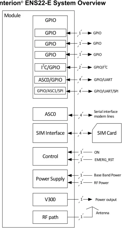
Cinterion
®ENS22-E System Overview
Figure 1: Cinterion® ENS22-E system overview
Module
ASC0
SIM Interface
Control
GPIO
GPIO
SIM Card
Power Supply
V300
GPIO GPIO Serial interface modem lines ON RF Power 1 4 1 1 1 1 1 Power output 1GPIO
GPIO EMERG_RSTBase Band Power 4
GPIO
RF path
1 1 AntennaASC0/GPIO
GPIO/ASC1/SPII
2C/GPIO
2 GPIO/I2C GPIO/UART 4 GPIO/UART/SPI 41.3
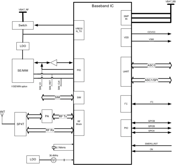
Circuit Concept
Figure 2 and Figure 3 show block diagrams of the Cinterion® ENS22-E module and illustrate
the major functional components.
Note: SE/MIM will be realized in future product release.
Figure 2: Cinterion® ENS22-E block diagram VREGI N_TX RF Block PIO PIO UART Baseband IC LDO Switch SE/MIM 38.4MHz 32.768kHz ※SE/MIN option ON EMERG_RST SMP IN VBAT_RF VDD CCVCC V300 SI M _I O SI M _ R S T SI M _ C LK VBAT_BB GPIO5 GPIO4 SIM SIM RF Tx PA ASC0 ASC1/SPI LDO GPIO8 SP4T RF Rx ANT I2C I2C
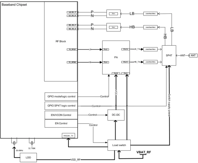
Figure 3: Cinterion® ENS22-E RF section block diagram Baseband Chipset RF Block HB_TX SP4T PA HB LDO 38.4MHz 32.768K Low-Pass Filter HB LB Load switch DC-DC VDD_RF GPIO mode/logic control
ANT ANT TX _RFHB TX_RFLB LB_TX Low-Pass Filter Low-Pass Filter Low-Pass Filter LB Pin2 Pin4 Pin11 Pin14 Balun Balun LB HB P N P N LB_RX _P LB _RX_N HB _RX_P HB _RX_N Control
GPIO SP4T logic control
VC C S w itc h s up ply p ow er VREGIN _TX
EN/VCON Control Control
EN Control
Pin12 Pin3
VBAT_RF
Control Control
2
Interface Characteristics
Cinterion® ENS22-E is equipped with an SMT application interface that connects to the external
application. The SMT application interface incorporates the various application interfaces as well as the RF antenna interface.
2.1
Application Interface
2.1.1
Pad Assignment
The SMT application interface on the Cinterion® ENS22-E provides connecting pads to
inte-grate the module into external applications. Figure 4 shows the connecting pads’ numbering plan. The following Table 1 lists the pads’ assignments.
2 1 3 4 5 6 7 8 9 10 11 12 13 14 15 16 17 18 19 51 52 50 49 48 47 46 45 44 43 42 41 40 39 38 37 36 35 34 75 76 21 20 23 22 25 24 27 26 29 28 31 30 33 32 65 66 63 64 61 62 59 60 57 58 55 56 53 54 77 78 79 80 74 68 69 70 71 72 73 67 101 102 103 104 105 106 100 94 95 96 97 98 99 93 90 89 86 85 92 91 88 87 84 83 82 81 Supply pads:
BATT+BB, BATT+RF GND pads SIM pads Combined GPIO/I
2C pads
Supply pads: Others ASC0 pads Do not useNC Combined GPIO/control Pads
Signal pads that are not used should not be connected to an external application.
Please note that the reference voltages listed in Table 2 are the values measured directly on the Cinterion® ENS22-E module. They do not apply to the accessories connected.
Table 1: Pad assignments
Pad no. Signal name Pad no. Signal name Pad no. Signal name
1 NC 24 NC 47 GND 2 NC 25 NC 48 GND 3 NC 26 NC 49 GND 4 GND 27 GPIO10/I2CDAT 50 GND 5 BATT+BB 28 GPIO9/I2CCLK 51 GND 6 GND 29 GPIO17/TXD1/SPI_MISO 52 GND 7 NC 30 GPIO16/RXD1/SPI_MOSI 53 BATT+RF 8 ON 31 GPIO18/RTS1/SPI_CLK 54 GND 9 GND 32 GPIO19/CTS1/SPI_CS 55 GND 10 V300 33 EMERG_RST 56 GND 11 RXD0 34 GND 57 GND 12 CTS0 35 Do not use1
1. Design reserved function, do not connect to any external application.
58 GND 13 TXD0 36 GPIO8 59 RF_OUT 14 GPIO24/RING0 37 NC 60-64 GND 15 RTS0 38 NC 65 NC 16 NC 39 GPIO5 66 NC 17 CCRST 40 GPIO4 67-74 GND
18 Do not use1 41 GPIO3/DSR0 75 NC
19 CCIO 42 GPIO2/DCD0 76 NC
20 CCVCC 43 GPIO1/DTR0 77-97 GND
21 CCCLK 44 NC 98 NC
22 NC 45 NC 99 GND
2.1.2
Signal Properties
Table 2: Signal propertiesFunction Signal name IO Signal form and level Comment Power
Supply BATT+BATT+BBRF
I VImax = 4.2V
VInorm = 3.6V
VImin = 3.1V
Cinterion® ENS22-E ports a lowest power sup-ply voltage of 2.8V, but some functions may degrade in RF and BB. For example, the output voltage of V300 may fall below 2.8V.
Minimum voltage must not fall below 2.8V, including drop, ripple, and spikes.
Power
Supply GND Ground Application Ground.
External Supply Voltage V300 O Normal operation: VOnorm = 3.0V IOmax = -5mA Ignition ON I VIHmax = 4.2V VIHnorm = 3.6V VIHmin = 2.8V VILmax = 0.6V
__|¯¯|__ high impulse width > 100ms
This signal switches on the module. Emer-gency Restart EMERG_RST I CI≈ 1nF VOHnorm = 3.0V VIHmin = 2.1V VILmax = 0.6V at ~10µA
¯¯|__|¯¯ low impulse width > 100ns
This line must be driven low by an open drain or open collector driver con-nected to GND.
Serial Interface ASC0 RXD0 O VOLmax = 0.3V VOHmin = 2.4V VOHmax = 3.3V
If unused keep lines open.
RXD0/TXD0 transferring only is not supported, unless RTS0 is set to low. RTS0 is mandatory if SLEEP or SUSPEND mode is needed for power saving.
Note that some ASC0 lines are configurable as GPIO lines. If configured as GPIO lines, the GPIO lines are assigned as fol-lows: GPIO1 --> DTR0 GPIO2 --> DCD0 GPIO3 --> DSR0 GPIO24 --> RING0 CTS0 O DSR0 O DCD0 O RING0 O TXD0 I VILmax = 0.6V VIHmin = 2.1V VIHmax = 3.3V RTS0 I DTR0 I Serial Interface ASC1 RXD1 O VOLmax = 0.3V VOHmin = 2.4V VOHmax = 3.3V VILmax = 0.6V VIHmin = 2.1V VIHmax = 3.3V
If unused keep line open. RXD1/TXD1 transferring only is not supported, unless RTS1 is set to low. Note that the ASC1 inter-face lines are originally available as GPIO lines. If configured as ASC1 lines, the GPIO lines are assigned as follows: GPIO16 --> RXD1 GPIO17 --> TXD1 GPIO18 --> RTS1 GPIO19 --> CTS1 If configured as SPI lines, the GPIO lines are assigned as follows: GPIO16 --> SPI_MOSI GPIO17 --> SPI_MISO GPIO18 --> SPI_CLK GPIO19 --> SPI_CS TXD1 I RTS1 I CTS1 O
Table 2: Signal properties
3V SIM Card Interface CCRST O VOLmax = 0.30V VOHmin = 2.4V VOHmax = 3.3V
Maximum cable length or copper track to SIM card holder should not exceed 100mm.
CCIO I/O VILmax = 0.3V VIHmin = 2.4V VIHmax = 3.3V VOLmax = 0.6V VOHmin = 2.1V VOHmax = 3.3V CCCLK O VOLmax = 0.30V VOHmin = 2.4V VOHmax = 3.3V CCVCC O VOmin= 2.7V VOtyp = 3.0V VOmax = 3.3V IOmax = -5mA 1.8V SIM Card Interface CCRST O VOLmax = 0.3V VOHmin = 1.44V VOHmax = 2.1V
Maximum cable length or copper track to SIM card holder should not exceed 100mm.
CCIO I/O VILmax = 0.36V VIHmin = 1.26V VIHmax = 1.98V VOLmax = 0.3V VOHmin = 1.44V VOHmax = 2.1V CCCLK O VOLmax = 0.3V VOHmin = 1.44V VOHmax = 2.1V CCVCC O VOmin = 1.5V VOtyp = 1.80V VOmax = 2.1V IOmax = -5mA
I2C I2CCLK IO Open drain IO External pull up voltage 3.0V
If lines are unused keep lines open.
Standard-mode bi-direc-tional bus (bit rate up to 100 kbit/s)
Note that the I2C inter- face lines are originally available as GPIO lines. If configured as I2C lines, the GPIO lines are assigned as follows: GPIO9 --> I2CCLK GPIO10 --> I2CDAT I2CDAT IO
SPI SPI_CLK O VOLmax = 0.3V VOHmin = 2.4V
VOHmax = 3.3V VILmax = 0.6V VIHmin = 2.1V
VIHmax = 3.3V
If lines are unused keep lines open.
Note that the SPI inter-face lines are originally available as GPIO and SPI lines.
If configured as ASC1 lines, the GPIO lines are assigned as follows: GPIO16 --> RXD1 GPIO17 --> TXD1 GPIO18 --> RTS1 GPIO19 --> CTS1 If configured as SPI lines, the GPIO lines are assigned as follows: GPIO16 --> SPI_MOSI GPIO17 --> MISO GPIO18 --> CLK GPIO19 --> SPI_CS SPI_MOSI O SPI_MISO I SPI_CS O GPIO
Interface GPIO1-GPIO3 IO VVOLOHmax = 0.3Vmin = 2.4V VOHmax = 3.3V
VILmax = 0.6V
VIHmin = 2.1V VIHmax = 3.3V
If unused keep line open. Please note that most GPIO lines can be config-ured by AT command for alternative functions: GPIO1-GPIO3: ASC0 control lines DTR0, DCD0 and DSR0. GPIO9/GPIO10: I2C GPIO16-GPIO19: ASC1 or SPI GPIO4 IO GPIO5 IO GPIO8 IO GPIO9-GPIO10 IO GPIO16-GPIO19 IO
Table 2: Signal properties
2.1.2.1
Absolute Maximum Ratings
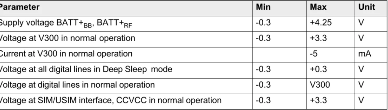
The absolute maximum ratings stated in Table 3 are stress ratings under any conditions. Stresses beyond any of these limits will cause permanent damage to Cinterion® ENS22-E.
Table 3: Absolute maximum rating
Parameter Min Max Unit
Supply voltage BATT+BB, BATT+RF -0.3 +4.25 V Voltage at V300 in normal operation -0.3 +3.3 V Current at V300 in normal operation -5 mA Voltage at all digital lines in Deep Sleep mode -0.3 +0.3 V Voltage at digital lines in normal operation -0.3 V300 V Voltage at SIM/USIM interface, CCVCC in normal operation -0.3 +3.3 V
2.1.3
Serial Interface ASC0
Cinterion® ENS22-E offers a high speed serial modem interface ASC0 for data exchange
between the module and the application.
Cinterion® ENS22-E is designed for an 8-wire unbalanced, asynchronous modem interface
ASC0 conforming to ITU-T V.24 protocol DCE signaling. The electrical characteristics do not comply with ITU-T V.28. The significant levels are 0V (for low data bit or active state) and 3V (for high data bit or inactive state). For electrical characteristics please refer to Table 2. For an illustration of the interface line’s startup behavior see Figure 5.
Cinterion® ENS22-E is designed for use as a DCE. Based on the conventions for DCE-DTE
connections it communicates with the customer application (DTE) using the following signals: • Port TXD @ application sends data to the module’s TXD0 signal line
• Port RXD @ application receives data from the module’s RXD0 signal line
Figure 5: Serial interface ASC0
Features:
• Includes the data lines TXD0 and RXD0, the status lines RTS0 and CTS0, in addition, the modem control lines DTR0, DSR0, DCD0 and RING0.
• The RING0 signal serves to indicate messages and other types of Unsolicited Result Codes (URCs). It can also be used to send pulses to the host application, for example to wake up the application from power saving state.
• Configured for 8 data bits, no parity and 1 stop bit (see AT+ICF in [1]). • ASC0 can be operated at fixed bit rates from 1,200bps up to 921,600bps.
• Wake up from SLEEP mode by RTS0 activation (high to low transition; see Section 3.3.4.1). Notes:
• The ASC0 modem control lines DTR0, DCD0, DSR0 and RING0 are configurable as GPIO lines. If configured as GPIO lines, these ASC0 lines are assigned as follows:
Configura-tance on the communication line.
• RXD0/TXD0 transferring only is not supported, unless RTS0 is set to low. • RTS0 is mandatory if SLEEP or SUSPEND mode is needed for power saving.
2.1.4
Serial Interface ASC1
Four Cinterion® ENS22-E GPIO lines can be configured as ASC1 interface signals to provide
a 4-wire unbalanced, asynchronous modem interface ASC1 conforming to ITU-T V.24 protocol DCE signaling. The electrical characteristics do not comply with ITU-T V.28. The significant lev-els are 0V (for low data bit or active state) and 3V (for high data bit or inactive state). For elec-trical characteristics please refer to Table 2. For an illustration of the interface line’s startup behavior see Figure 6.
The ASC1 interface lines are originally available as GPIO lines. If configured as ASC1 lines, the GPIO lines are assigned as follows: GPIO16 --> RXD1, GPIO17 --> TXD1, GPIO18 --> RTS1 and GPIO19 --> CTS1. If configured as SPI lines, the GPIO lines are assigned as fol- lows:GPIO16 --> SPI_MOSI, GPIO17 --> SPI_MISO, GPIO18 --> SPI_CLK, GPIO19 --> SPI_CS. The configuration is non-volatile and becomes active after a module restarts.
Cinterion® ENS22-E is designed for use as a DCE. Based on the conventions for DCE-DTE
connections it communicates with the customer application (DTE) using the following signals: • Port TXD @ application sends data to module’s TXD1 signal line
• Port RXD @ application receives data from the module’s RXD1 signal line
Figure 6: Serial interface ASC1
Features
• Includes only the data lines TXD1 and RXD1 plus RTS1 and CTS1 for hardware hand-shake.
• On ASC1 no RING line is available.
• Configured for 8 data bits, no parity and 1 stop bits (see AT+ICF in [1]). • ASC1 can be operated at fixed bit rates from 1,200 bps to 921,600 bps. Notes:
• It is not supported to wake up the module from SLEEP mode by RTS1. Always wake up the module by RTS0 (high to low transition; see Section 3.3.4.1). To use ASC1, keep RTS0 low to ensure the module stays awake.
• In order to adjust overshoot and undershoot, it is recommended to increase matching resis-tance on the communication line.
2.1.5
UICC/SIM/USIM Interface
Cinterion® ENS22-E has an integrated UICC/SIM/USIM interface that is wired to the host
inter-face in order to be connected to an external SIM card holder. Four pads on the SMT application interface are reserved for the SIM interface.
The UICC/SIM/USIM interface supports 3V and 1.8V SIM cards. Please refer to Table 2 for electrical specifications of the UICC/SIM/USIM interface lines depending on whether a 3V or 1.8V SIM card is used.
The figure below shows a circuit to connect an external SIM card holder.
Figure 7: External UICC/SIM/USIM card holder circuit
To avoid possible cross-talk from the CCCLK signal to the CCIO signal, be careful that both lines are not placed closely next to each other. A useful approach is using a GND line to shield the CCIO line from the CCCLK line.
An example for an optimized ESD protection for the SIM interface is shown in Section 2.1.5.1.
Table 4: Signals of the SIM interface (SMT application interface)
Signal Description
GND Separate ground connection for SIM card to improve EMC CCCLK Chipcard clock
CCVCC SIM supply voltage
CCIO Serial data line, input and output CCRST Chipcard reset
2.1.5.1
Enhanced ESD Protection for SIM Interface
To optimize ESD protection for the SIM interface it is possible to add ESD diodes to the SIM interface lines as shown in the example given in Figure 8.
The example was designed to meet ESD protection according ETSI EN 301 489-1: Contact dis-charge: ± 4kV, air disdis-charge: ± 8kV.
2.1.6
GPIO Interface
Cinterion® ENS22-E offers a GPIO interface with 13 GPIO lines. The GPIO lines are shared
with other interfaces or functions: the I2C functionality (see Section 2.1.7), ASC0 (see Section
2.1.3), ASC1 (see Section 2.1.4), an SPI interface (see Section 2.1.8).
The following table shows the configuration variants for the GPIO pads.
After startup, the above mentioned alternative GPIO line assignments can be configured using AT commands (see [1]).
Table 5: GPIO lines and possible alternative assignment
GPIO I2C ASC0 ASC1 SPI
GPIO1 DTR0 GPIO2 DCD0 GPIO3 DSR0 GPIO4 GPIO5 GPIO8 GPIO9 I2CCLK GPIO10 I2CDAT GPIO16 RXD1 SPI_MOSI GPIO17 TXD1 SPI_MISO GPIO18 RTS1 SPI_CLK GPIO19 CTS1 SPI_CS GPIO24 RING0
2.1.7
I
2C Interface
I2C is a serial, 8-bit oriented data transfer bus. It is available in the Active and Standby modes.
• Standard mode bi-directional bus (bit rate up to 100Kbit/s)
• Operation either as a master, but not as a master in a multi-master system • 7-bit addressing
• Clock Stretching detect and generation
• Transmissions/Reception of data up to maximum 16 bytes
To configure and activate the I2C bus, use the AT^SSPI command. Detailed information on the
AT^SSPI command, as well as explanations on the protocol and syntax required for data trans-mission, can be found in [1].
The I2C interface requires external pull-up resistors. The range of allowed values for the pull up
resistors depends on the IO voltage used and the total bus capacitance. A value towards the high end of the range is recommended in order to minimize power consumption.
Notes:
• Pay attention when creating the PCB layout of the host application. The traces of I2CCLK and I2CDAT should be equal in length and as short as possible.
• In order to adjust overshoot and undershoot, it is recommended to increase matching resis-tance on the communication line.
2.1.8
SPI Interface
Four Cinterion® ENS22-E GPIO interface lines can be configured as Serial Peripheral Interface
(SPI). The SPI is a synchronous serial interface for control and data transfer between Cinteri-on® ENS22-E and the external application. Only one application can be connected to the SPI
and the interface supports only master mode. The transmission rates are up to 800Kbps. The SPI interface comprises the two data lines SPI_MOSI and SPI_MISO, the clock line SPI_CLK, as well as the chip select line SPI_CS.
• Data transfer rate up to 800kbps
• Only support transfer Mode 0 (CPOL=0 CPHA=0)
• Transmissions/Reception of data up to a maximum of 128 bytes • SPI master operation
The four GPIO lines can be configured as SPI interface signals as follows:
GPIO16 --> SPI_MOSI, GPIO17 --> MISO, GPIO18 --> CLK, and GPIO19 --> SPI_CS. The configuration is done by AT command (see [1]). It is non-volatile and becomes active after a module restart.
The GPIO lines are also shared with the ASC1 signal.
To configure and activate the SPI interface, use the AT^SSPI command. Detailed information on the AT^SSPI command, as well as explanations on the SPI modes required for data trans-mission, can be found in [1].
Note: In order to adjust overshoot and undershoot, it is recommended to increase matching re-sistance on the communication line.
2.1.9
Control Signals
2.1.9.1
Power Indication Circuit
In Power Down mode or SUSPEND mode, all digital pins are unpowered. Pulling these pins high will cause current leakage.
It is recommended to implement a power indication signal that reports the module’s power state and shows whether it is active, in Power Down mode, or in SUSPEND mode. While the module is in Power Down mode or SUSPEND mode, all signals with a high level from an external ap-plication need to be set to low state or high impedance state. The sample power indication cir-cuit illustrated in Figure 9denotes the module’s active state with a low signal, and the module’s Power Down and SUSPEND modes with a high signal or high impedance state.
Figure 9: Power Indication Circuit
Note: V300 will be off in firmware update, so V300 cannot indicate the state of the circuit when the firmware is upgrading.
2.2
RF Antenna Interface
Cinterion® ENS22-E is an integrated NB-IoT transceiver, with necessary features to enable
multi-mode, multi-band mobile cellular devices. The module can operate over 698-960 MHz and 1695-2180MHz with a 200 kHz system bandwidth. It is designed to communicate with mo-bile network operator (MNO) infrastructure equipment using the 3GPP NB-IoT radio protocol. The RF interface has an impedance of 50Ω. Cinterion® ENS22-E is capable of sustaining a total
mismatch at the antenna lines without any damage, even when transmitting at maximum RF power.
The external antenna must be matched properly to achieve best performance regarding radi-ated power, modulation accuracy and harmonic suppression. Antenna matching networks are not included on the Cinterion® ENS22-E module and should be placed in the host application
if the antenna does not have an impedance of 50Ω.
Regarding the return loss, Cinterion® ENS22-E provides the following values in the active band:
Table 6: Return loss in the active band
State of module Return loss of module Recommended return loss of application Receive > 8dB > 12dB
2.2.1
Antenna Interface Specifications
Table 7: RF Antenna interface (at operating temperature range)Parameter Conditions Min. Typical Max. Unit
Cat NB1 connectivity Band 3, 5, 8, 20, 28 Cat NB1 Frequency range
Uplink (UE Tx) NB-IoT Band 3 1710 1785 MHz
NB-IoT Band 5 824 849 MHz
NB-IoT Band 8 880 915 MHz
NB-IoT Band 20 832 862 MHz
NB-IoT Band 28 703 748 MHz
Cat NB1 Frequency range
Downlink (UE Rx) NB-IoT Band 3 1805 1880 MHz
NB-IoT Band 5 869 894 MHz
NB-IoT Band 8 925 960 MHz
NB-IoT Band 20 791 821 MHz
NB-IoT Band 28 758 803 MHz
Cat NB1
Receiver Input Sensitivity without repetitions -40°C ≤Board temperature ≤85°C NB-IoT Band 3 -114 dBm NB-IoT Band 5 -114 dBm NB-IoT Band 8 -114 dBm NB-IoT Band 20 -114 dBm NB-IoT Band 28 -114 dBm Cat NB1
RF Power @ ARP with 50Ω
Load -40°C ≤Board temperature ≤85°C NB-IoT Band 3 21.3 23 24.7 dBm NB-IoT Band 5 21.3 23 24.7 dBm NB-IoT Band 8 21.3 23 24.7 dBm NB-IoT Band 20 21.3 23 24.7 dBm NB-IoT Band 28 21.3 23 24.7 dBm
2.2.2
Antenna Installation
Figure 10 shows mechanical description of antenna interface. The antenna interface is typically connected by soldering the antenna pad (RF_OUT, Pad No. 59) directly to the application's PCB. Antenna interface allows to make a simple transition to different types of 50Ω lines.
Figure 10: Antenna pads (dimensions in mm)
The distance between the antenna pad and its neighboring GND pads has been optimized for best possible impedance. To prevent mismatch, special attention should be paid to these pads on the application‘s PCB.
The wiring of the antenna connection, starting from the antenna pad to the application‘s anten-na should result in a 50Ω line impedance. Line width and distance to the GND plane needs to be optimized with regard to the PCB’s layer stack.
To prevent receiver desensitization due to interferences generated by fast transients like high speed clocks on the external application PCB, it is recommended to realize the antenna con- nection line using embedded Stripline rather than Micro-Stripline technology. Please see Sec-tion 2.2.3 for how to design the antenna connecSec-tion in order to achieve the required 50Ω line impedance.
For type approval purposes, the use of a 50Ω coaxial antenna connector (U.FL-R-SMT) might be necessary. In this case the U.FL-R-SMT connector should be placed as close as possible to Cinterion® ENS22-E‘s antenna pad.
53 65 64 63 62 61 60 59 58 57 56 55 54 66 33 21 22 23 24 25 26 27 28 29 30 31 32 20 106 92 91 98 97 96 95 94 90 89 85 86 93 74 99 87 88 84 83 79 78 77 76 75 82 81 80 72 71 70 69 68 67 105 104 103 102 101 100 73 44 19 18 17 16 15 14 13 12 11 10 9 8 7 6 5 4 3 2 1 34 35 36 37 38 39 40 41 42 43 45 46 47 48 49 50 51 52 GND GND RF_OUT
#58
#59
#60
0.81 0.48 0.48 1.52.2.3
RF Line Routing Design
2.2.3.1
Line Arrangement Examples
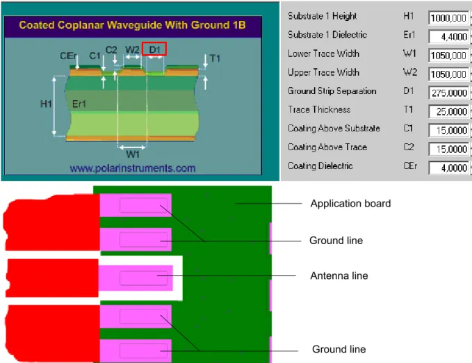
Several dedicated tools are available to calculate line arrangements for specific applications and PCB materials - for example from http://www.polarinstruments.com/ (commercial software) or from http://web.awrcorp.com/Usa/Products/Optional-Products/TX-Line/ (free software). Embedded Stripline
Figure 11 shows a line arrangement example for embedded stripline with 65µm FR4 prepreg (type: 1080) and 710µm FR4 core (4-layer PCB).
Micro-Stripline
This section gives two line arrangement examples for micro-stripline. • Micro-Stripline on 1.0mm Standard FR4 2-Layer PCB
The following two figures show examples with different values for D1 (ground strip separa-tion).
Figure 12: Micro-Stripline on 1.0mm standard FR4 2-layer PCB - Example 1
Antenna line Ground line
Ground line Application board
Figure 13: Micro-Stripline on 1.0mm Standard FR4 PCB - Example 2
Antenna line Ground line
Ground line Application board
• Micro-Stripline on 1.5mm Standard FR4 2-Layer PCB
The following two figures show examples with different values for D1 (ground strip separa-tion).
Figure 14: Micro-Stripline on 1.5mm Standard FR4 PCB - Example 1
Antenna line Ground line
Ground line Application board
Figure 15: Micro-Stripline on 1.5mm Standard FR4 PCB - Example 2
Antenna line Ground line
Ground line Application board
2.2.3.2
Routing Example
Figure 16 shows the connection of the module‘s antenna pad with an application PCB‘s coaxial antenna connector. Please note that the Cinterion® ENS22-E bottom plane appears mirrored,
since it is viewed from Cinterion® ENS22-E top side. By definition the top of customer's board
shall mate with the bottom of the Cinterion® ENS22-E module.
2.3
Sample Application
Figure 17 shows a typical example of how to integrate a Cinterion® ENS22-E module with an
application. Usage of the various host interfaces depends on the desired features of the appli-cation.
Because of the very low power consumption design, current flowing from any other source into the module circuit must be avoided, for example reverse current from high state external control lines. Therefore, the controlling application must be designed to prevent reverse current flow. Otherwise there is the risk of undefined states of the module during startup and shutdown or even of damaging the module.
Since the module is running at high RF power, it is designed to avoid self-interference inside the module. Customer application design must also use the best practices to avoid self inter-ference.
While developing SMT applications it is strongly recommended to provide test points for certain signals, i.e., lines to and from the module - for debug and/or test purposes. The SMT application should allow for an easy access to these signals. For details on how to implement test points, see [4].
The EMC measures are best practice recommendations. In fact, an adequate EMC strategy for an individual application is very much determined by the overall layout and, especially, the po-sition of components.
Depending on the micro controller used by an external application, Cinterion® ENS22-E‘s
dig-ital input and output lines may require level conversion.
Note: Cinterion® ENS22-E is not intended for use with cables longer than 3m.
Disclaimer
No warranty, either stated or implied, is provided on the sample schematic diagram shown in Figure 17 and the information detailed in this section. As functionality and compliance with na-tional regulations depend to a great amount on the used electronic components and the indi-vidual application layout manufacturers are required to ensure adequate design and operating safeguards for their products using Cinterion® ENS22-E modules.
Figure 17: Schematic diagram of Cinterion® ENS22-E sample application ENS22 ON 100K EMERG_RST RESET V300 Output current <5mA
Blocking*** Blocking*** ASC0 8 4 ASC1 SIM CCVCC CCIO CCRST CCCLK 220n 1n GN D GN D GN D GN D RF_OUT GND GND 47uF** 33pF 47uF** 33pF BATT+RF
BATT+BB Power Supply
Blocking*** GPIO 5
Beads*
Blocking***: see 3.7 Blocking against RF on Interface Lines
Beads*: It is recommended to add beads as shown to the BATT _BB line.
47uF**: Pay attention to leakage current of capacitor. It is recommend ed to use low power capacitor.
2.3.1
Sample Level Conversion Circuit
The following signals are mandatory for using the ASC0 and/or ASC1 interface.
Table 8: Mandatory signals for ASC0 and ASC1
For these signals mentioned in Table 8, several circuits are recommended as following. 1. If the IO domain of the application is 3V, the signals mentioned in Table 8 can be connected
via a serial resistor directly. See Figure 18.
Table 9 contains additional signals which need a level conversation. See Figure 20.
Note: This circuit is highly recommended for ultra-low power and cost optimized designs.
Pad No. Signal name Description
11 RXD0 ASC0 RXD line
12 CTS0 ASC0 CTS line
13 TXD0 ASC0 TXD line
14 GPIO24/RING0 ASC0 RING line, shared with GPIO
15 RTS0 ASC0 RTS line
29 GPIO17/TXD1/SPI_MISO ASC1 TXD line, shared with GPIO and SPI 30 GPIO16/RXD1/SPI_MOSI ASC1 RXD line, shared with GPIO and SPI 31 GPIO18/RTS1/SPI_CLK ASC1 RTS line, shared with GPIO and SPI 32 GPIO19/CTS1/SPI_CS ASC1 CTS line, shared with GPIO and SPI
External application VLOGIC (3.0V) µTXD0 µRTS0 µTXD1 µRTS1 µRXD0 µCTS0 µRING0 µRXD1 µCTS1 ENS22 module TXD0 RTS0 TXD1 RTS1 RXD0 CTS0 RING0 RXD1 CTS1 MCU R R R R R R R R R
2. If the IO domain of the application is not 3V the signals mentioned in Table 8 and Table 9 need level conversation. See Figure 19 or Figure 20.
Figure 19: Sample level conversion circuit for Table 8 signals
Figure 19 illustrates the possible design of a 3V0 LDO, e.g. RP118x with 0.2uA (typical) for qui-escent dissipation, and the switching state of LDO is controlled by MCU. The power supply volt-age of TXD0 (ASC0's TXD signal line) in Figure 19 must be supplied by an external 3V LDO because in firmware update mode V300 is powered off. Do not use V300 related functions as the enablement of level conversion, e.g. power indicator (see Section 2.1.9.1).
VCC External application µGPIO µTXD0 Output lines, e.g., µRTS0, µTXD1, µRTS1 VLOGIC (1.8V...3.6V) Input lines, e.g., µRXD0, µCTS0, µRING0, µRXD1, µCTS1 ENS22 module BATT+BB TXD0 V300 (3.0V)
Digital input lines, e.g., RTS0, TXD1, RTS1
Digital output lines, e.g., RXD0, CTS0, RING0, RXD1, CTS1 MCU VCC 3V0 E.g. SN74LVC2G34 E.g. SN74LVC1G34 E.g. SN74LVC2G34 BATT+BB VDD CE E.g. RP118x series VO 3V0
In order to prevent back-feeding, the level conversion circuit must be added when the signals mentioned in Table 9 are used:
Note: Even if the power supply voltage of MCU is 3V, the level conversion circuit is recom-mended for preventing back-feeding of Table 9 pins. Power supply of digital input lines must be V300. Figure 20 shows an universal circuit that is not optimized for ultra-low current con-sumption.
Figure 20: Universal level conversion circuit for Table 9 signals
Table 9: Table of signals with required level conversion
Pad No. Signal name Description
27 GPIO10/I2CDAT I2C data line, shared with GPIO 28 GPIO9/I2CCLK I2C clock line, shared with GPIO
36 GPIO8 GPIO
39 GPIO5 GPIO
40 GPIO4 GPIO
41 GPIO3/DSR0 ASC0 DSR line, shared with GPIO 42 GPIO2/DCD0 ASC0 DCD line, shared with GPIO 43 GPIO1/DTR0 ASC0 DTR line, shared with GPIO
External application VLOGIC (1.8V...3.6V) Input lines, e.g., µDCD0, µDSR0 Output lines, e.g., µDTR0 VCC ENS22 module
Digital output lines, e.g., DCD0, DSR0 V300 (3.0V)
Digital input lines, e.g., DTR0 VCC MCU E.g. SN74LVC2G34 E.g. SN74LVC2G34
3
Operating Characteristics
3.1
Operating Modes
The table below briefly summarizes the various operating modes referred to throughout the document.
Table 10: Overview of operating modes
Mode Function Normal
operation Active TX NB-IoT data transfer in progress. Power consumption depends on network settings, data transfer rate and radio conditions. IDLE No data transfer is in progress. The NB-IoT part of the device can be
in NB-IoT DRX, NB-IoT eDRX or NB-IoT PSM mode. Activity on ASC0 /ASC1 interfaces can be present. Power consumption depends on the NB-IoT power saving mode and its parameters and on the activity on the ASC interfaces.
SLEEP The module is in low power consumption state. There is no activity inside the module but module preserves the state in which it was before entering the SLEEP mode, including the electrical states of the GPIOs. To allow SLEEP mode, the host application shall indi-cate via RTS0 line that it has no intention to send data.
SUSPEND The module is in the lowest power consumption state, in which the module is still regis-tered to the network. There is no activity inside the module unless the internal counter and circuit for wake-up mechanism. The module does not preserve the state in which it was before entering the SUSPEND mode, including the GPIOs.
The module shall enter SUSPEND mode only when the NB-IoT eDRX or NB-IoT PSM is enabled (i.e. configuration negotiated with the network allows it). To allow SUSPEND mode, the host application shall indicate via RTS0 line that it has no intention to send data. Device wakeup can be available via the ON Signal. Host wakeup can be available via RING0.
Power
3.2
Power Up/Power Down Scenarios
In general, be sure not to turn on Cinterion® ENS22-E while it is beyond the safety limits of
volt-age and temperature stated in Section 2.1.2.1 and Section 3.5. Cinterion® ENS22-E
immedi-ately switches off after having started and detected these inappropriate conditions. In extreme cases this can cause permanent damage to the module.
3.2.1
Turn on Cinterion
®ENS22-E
After the operating voltage BATT+ is applied, Cinterion® ENS22-E can be switched on by means
of the ON signal.
The ON signal is a high active pulse signal. Its range of input voltage level is from 2.8V to 4.2V, and the control signal of external application can be BATT+, GPIO from MCU, or other signals which can fulfill the requirement of an input voltage range of 2.8V to 4.2V. The module starts into normal mode on detecting a high level at the ON signal. It is recommended to use high level pulse of a minimum 100 ms. The following Figure 21 shows ON pin connection.
Figure 21: ON pin connection
ENS22 Module Baseband Chipset 33k 100k ON
The Figure 22 shows options for possible switch-on circuits.
Figure 22: ON circuit options
With Option 2, the typical resistor values are: R1 = 150k and R2 = 22k. Note that the resistor values depend on the current gain from the employed PNP resistor.
Figure 23 shows the timing sequence when the module starts up. When the battery powers up, normally, it should wait at least 5 seconds before using ON function.
Figure 23: ON timing
Auto enabled level**: V300 rail is automatically enabled at the lowest voltage (1.5V) when module is pow-ered on. This lowest voltage will be disabled immediately after the module’s firmware boots up. V300 turns to normally voltage (3V) after the ON signal is triggered.
External application ENS22 Module ON MCU µGPIO R Input voltage: 2.8V to 4.2V BATT+ R1 R2 Switch Option2 Option1 t1,delay>5s t2,duty>100ms t3,startup>150ms BATT+ EMERG_RST ON
3.2.2
Restart Cinterion
®ENS22-E
After startup Cinterion® ENS22-E can be re-started as described in the following sections:
• Software controlled reset by AT+CFUN command: Starts Normal mode (see Section 3.2.2.1).
• Hardware controlled reset by EMERG_RST line: Starts Normal mode (see Section 3.2.2.2).
3.2.2.1
Restart Cinterion
®ENS22-E via AT+CFUN Command
To reset and restart the Cinterion® ENS22-E module use the command AT+CFUN. See [1] for
details.
3.2.2.2
Restart Cinterion
®ENS22-E Using EMERG_RST
The EMERG_RST signal is internally connected to the baseband chipset. A low level for more than 100ns sets the processor into a reset state. After releasing the EMERG_RST line (i.e., with a change of the signal level from low to high), the module restarts.
Figure 24: Emergency reset timing
It is recommended to control this EMERG_RST line with an open collector transistor or an open drain field-effect transistor (FET).
Caution: Use the EMERG_RST line only when, due to serious problems, the software is not responding for more than 10 seconds. Pulling the EMERG_RST line causes the loss of all in-formation stored in the volatile memory. Therefore, this procedure is intended only for use in case of emergency, e.g., if Cinterion® ENS22-E does not respond, if reset or shutdown via AT
command fails. Ignition BATT+ EMERG_RST ON V300 System started >100ns Reset state System started again 5s
3.2.3
Turn off Cinterion
®ENS22-E
To switch off the module, the following procedures may be used:
• Software controlled shutdown procedure: Software controlled by sending an AT command
over the serial application interface. See Section 3.2.3.1.
• Automatic shutdown (software controlled): Takes effect if module’s board temperature or
voltage levels exceed a critical limit. See Section 3.2.4.
3.2.3.1
Switch off Cinterion
®ENS22-E Using AT Command
The best and safest approach to powering down Cinterion® ENS22-E is to issue the
appropri-ate AT command. This procedure lets Cinterion® ENS22-E log off from the network and allows
the software to enter into a secure state and safe data before disconnecting the power supply. The mode is referred to as Power Down mode. In this mode, only the RTC stays active. After sending the switch off command AT^SMSO, be sure not to enter any further AT commands un-til the module was restarted.
While Cinterion® ENS22-E is in Power Down mode the application interface is switched off and
must not be fed from any other voltage source. Therefore, your application must be de-signed to avoid any current flow into any digital pads of the application interface.
3.2.4
Automatic Shutdown
Automatic shutdown takes effect if the following event occurs:
• Cinterion® ENS22-E board is exceeding the critical limits of overtemperature or
undertem-perature (see Section 3.2.4.1)
• Undervoltage or overvoltage is detected (see Section 3.2.4.2 and Section 3.2.4.3)
The automatic shutdown procedure is equivalent to the power-down initiated with an AT com-mand, i.e. Cinterion® ENS22-E logs off from the network and the software enters a secure state
avoiding loss of data.
3.2.4.1
Thermal Shutdown
The board temperature is constantly monitored by an internal temperature sensor located on the PCB. The values detected by the temperature sensor are measured directly on the board and therefore, are not fully identical with the ambient temperature.
Each time the board temperature goes out of range or back to normal, Cinterion® ENS22-E
in-stantly displays an alert (if enabled).
• URCs indicating the level "-1" allow the user to take appropriate precautions, such as pro-tecting the module from exposure to extreme conditions. The presentation of the URCs depends on the settings selected with the AT^SCTM write command (for details see [1]): AT^SCTM=1: Presentation of URCs is always enabled.
AT^SCTM=0 (default): The presentation of URCs is disabled, i.e. no URCs with alert levels ''-1" will be generated.
• URCs indicating the level "2" or "-2" are instantly followed by an orderly shutdown. The pre-sentation of these URCs is always enabled, i.e. they will be output even though the factory setting AT^SCTM=0 was never changed.
The maximum temperature ratings are stated in Section 3.5. Refer to Table 11 for the associ-ated URCs.
Table 11: Temperature dependent behavior
Sending temperature alert (only if URC presentation enabled) ^SCTM_B: -1 Board close to undertemperature limit. ^SCTM_B: 0 Board back to non-critical temperature range.
Automatic shutdown (URC appears no matter whether or not presentation was enabled)
^SCTM_B: 2 Alert: Board equal or beyond overtemperature limit. Cinterion® ENS22-E switches off.
^SCTM_B: -2 Alert: Board equal or below undertemperature limit. Cinterion® ENS22-E switches off.
3.2.4.2
Undervoltage Shutdown
The undervoltage shutdown threshold is the specified minimum supply voltage VBATT+ given in Table 15. When the average supply voltage measured by Cinterion® ENS22-E approaches the
undervoltage warning threshold, the module will send the following URC: ^SBC: Undervoltage warning
The undervoltage warning is sent only once - until the next time the module is close to the un-dervoltage shutdown threshold.
Note: For external applications operating at the limit of the allowed tolerance, the default un-dervoltage warning threshold may be adapted by subtracting an offset. For details see [1]: AT^SCFG= "MEShutdown/sVsup/threshold".
If the voltage continues to drop below the specified undervoltage shutdown threshold, the mo-dule will send the following URC:
^SBC: Undervoltage shutdown
This undervoltage shutdown is sent only once before the module shuts down cleanly without sending any further messages.
This type of URC does not need to be activated by the user. It will be output automatically when fault conditions occur.
3.2.4.3
Overvoltage Shutdown
The overvoltage shutdown threshold is the specified maximum supply voltage VBATT+ given in Table 15. When the average supply voltage measured by Cinterion® ENS22-E approaches the
overvoltage warning threshold (i.e. 0.1V offset) the module will send the following URC: ^SBC: Overvoltage Warning
The overvoltage warning is sent only once - until the next time the module is close to the over-voltage shutdown threshold.
If the voltage continues to rise above the specified overvoltage shutdown threshold, the module will send the following URC:
^SBC: Overvoltage Shutdown
This alert is sent only once before the module shuts down cleanly without sending any further messages.
This type of URC does not need to be activated by the user. It will be output automatically when fault conditions occur.
3.3
Power Saving while Attached to NB-IoT
Cinterion® ENS22-E can be configured to control power consumption by DRX, eDRX, and PSM
while attached to an NB-IoT network. PSM is the recommended and efficient way of power sa-ving.
Generally, power saving depends on the module’s application scenario and may differ from the following normal operation.
3.3.1
Power Saving in DRX
Cinterion® ENS22-E can be configured to use DRX (Discontinuous Reception) in idle mode to
reduce power consumption. The power saving possibilities while attached to an NB-IoT net-work depend on the paging timing cycle of the base station.
During normal NB-IoT operation, i.e., the module is connected to an NB-IoT network, the dura-tion of power saving period varies. It may be calculated using the following formula:
t = DRX Cycle Value * 10 ms
DRX cycle value in NB-IoT networks is any of the four values: 128, 256, 512 and 1024, thus resulting power saving intervals between 1.28 and 10.24 seconds. The DRX cycle value of the base station is assigned by the NB-IoT network operator.
In the pauses between listening to paging messages, the module resumes power saving, as shown in Figure 25.
Figure 25: DRX in NB-IoT networks
The varying pauses explain the different potential for power saving. The longer the pause the less power is consumed.
3.3.2
Power Saving in eDRX
Cinterion® ENS22-E and the network may negotiate the use of eDRX (extended DRX) to
reduce power consumption, while being available for mobile terminating data and/or network originated procedures within a certain delay dependent on the DRX cycle value. If the network is configured to use eDRX, the module only monitors the Paging messages, during a periodic Paging Time Window (PTW) configured for Cinterion® ENS22-E.
The eDRX cycle length is mapped according to Table 12.
The value range starts from 20.48s up to a maximum of 10485.76s (almost 3 hours). The PTW length can be calculated using the following formula:
t_ptw = (PTW value +1)* 2560 ms
Figure 26 shows the eDRX procedure, with the module listening to paging messages in paging time window.
Table 12: eDRX cycle length mapping table
eDRX value (binary code) E-UTRAN eDRX cycle length duration (seconds)
0010 20.48 0011 40.96 0101 81.92 1001 163.84 1010 327.68 1011 655.36 1100 1310.72 1101 2621.44 1110 5242.88 1111 10485.76
3.3.3
Power Saving in PSM
Cinterion® ENS22-E can be configured to use Power Saving Mode (PSM) to reduce power
con-sumption. The PSM is similar to power off, while Cinterion® ENS22-E remains registered with
the network. There is no need to re-attach or re-establish PDN connections. Cinterion®
ENS22-E in PSM is not immediately reachable for mobile terminating services.
The network accepts the use of PSM by providing a specific value for active timer (T3324). Upon expiry of the active timer, or if the value provided by the network is zero, Cinterion®
ENS22-E may activate PSM.
NOTE: If Cinterion® ENS22-E requests to enable both PSM (requesting an active time and
pos-sibly a periodic TAU timer) and eDRX (with a specific extended idle mode DRX cycle value), it is up to the network to decide whether to:
1. Enable only PSM, i.e. not accept the request for extended idle mode DRX.
2. Enable only extended idle mode DRX, i.e. not accept the request for an active time.
3. Enable both PSM (i.e. provide an active time) and extended idle mode DRX (i.e. provide an extended idle mode DRX parameters).
Cinterion® ENS22-E monitors paging message in the active timer, according to the eDRX/DRX
setting. If the module has uplink data or signal, it will be out of PSM.
Figure 27 shows the module procedure, when the network enable PSM and eDRX simultane-ously.
Figure 27: Enable eDRX and PSM in NB-IOT networks
The active timer and periodic Tracking Area Update (TAU) timer can be configured by
AT+CPSMS command. The timer value is only one byte: bit5~1 indicate the value, bit8~6 indi-cate the timer unit.
The timer unit is mapped according to Table 13 and Table 14.
Table 13: Active timer unit mapping table
Active timer value (bit 8~6) Active timer unit
000 2 seconds
001 1 minute
010 Decihour (6 minutes)
111 The timer is deactivated
Table 14: Periodic TAU timer unit mapping table
Periodic TAU timer value (bit 8~6) Periodic TAU timer unit
000 10 minutes 001 1 hour 010 10 hours 011 2 seconds 100 30 seconds 101 1 minute 110 320 hours
3.3.4
Power Saving in SLEEP and SUSPEND Modes
Cinterion® ENS22-E supports the following low consumption modes:
• SLEEP mode: A low energy consumption mode. There is no activity inside the module but module preserves the state in which it was before entering the SLEEP mode, including the electrical states of the GPIOs. See Section 3.3.4.1.
• SUSPEND mode: The lowest energy consumption mode of Cinterion® ENS22-E, in which
the module is still registered to the network. There is no activity inside the module unless the internal counter and circuit for wake-up mechanism. See Section 3.3.4.2.
Figure 28 shows how Cinterion® ENS22-E transits between different states and modes.
Figure 28: State Transition of Cinterion® ENS22-E Notes:
• When all UART interfaces (i.e. ASC0 and ASC1) are idle, the module enters SLEEP or SUSPEND mode by keeping RTS0 high for 5 seconds.
• The UART interfaces are not idle if there is any response message not read out from ASC0 or ASC1. SUSPEND SLEEP POWER DOWN RING0 (URC or DATA) RING0 (URC or DATA) AT^SCFG AND UART Inactive ON Signal NO DATA, RRC Release Paging or DATA UART Inactive UART Active AT+SMSO ON Signal IDLE ACTIVE
3.3.4.1
SLEEP Mode
By default, the module enters SLEEP mode if RTS0 is inactive (i.e. UART inactive) for a time interval of 5 seconds. The time interval is configurable by AT^SPOW. See [1] for details. RTS0 can be used to wake up Cinterion® ENS22-E from SLEEP mode configured with
AT^SPOW. Assertion of RTS0 (i.e. toggle from inactive high to active low) serves as wake up event, thus allowing an external application to almost immediately terminate power saving. After RTS0 assertion, the CTS0 line signals module wake up, i.e. readiness of the AT com-mand interface.
Note: After the assertion of RTS0, there is a minor time interval (<5ms) before the UART is ready (CTS0 is low). In this interval, data on the UART will be truncated.
When RTS0 is de-asserted, after UART is inactive for a configured time interval, the module will return to SLEEP mode again and de-assert the CTS0.
It is therefore recommended to enable RTS/CTS flow control (default setting). Figure 29 shows the described RTS0 wake up mechanism.
3.3.4.2
SUSPEND Mode
The command AT^SCFG=”MeOpMode/PowerMgmt/Suspend”, <Suspend> enables the SUS-PEND mode in Cinterion® ENS22-E. See [1] for details.
Cinterion® ENS22-E shall enter SUSPEND mode if PSM or eDRX is enabled (i.e. configuration
negotiated with the network allows it).
Once the SUSPEND mode is enabled via AT command, and network negotiated parameters allow energy gaining from the SUSPEND mode, the following URC shows:
"^SUSPEND AVAILABLE"
In addition, if no more communication with network is needed, the module is ready to enter SUSPEND mode, the following URC shows:
"^SUSPEND READY"
If RTS0 is set to inactive (i.e. UART inactive) for a configured time interval, the module enters SUSPEND mode. The length of time interval is configurable using AT^SPOW. See [1] for de-tails.
If the module enters SUSPEND mode, SPI or I2C shall be disconnected.
In SUSPEND mode, Power Indication Circuit (refer to Section 2.1.9.1) can report the module’s power state (i.e. whether in SUSPEND mode).
Figure 30 shows the handshake between the host, module and network for entering SUSPEND mode.
Figure 30: Handshake for entering SUSPEND mode
Network confirms PSM/eDRX and Assigns Timers
MODULE
HOST NETWORK
Host Enables SUSPEND <AT^SCFG:"SUSPEND"> Host Request Timers <AT+CPSMS or AT+CEDRXS>
Module requests PSM/eDRX and Desired Timers
SUSPEND possible ^SUSPEND AVAILABLE Module ready to go SUSPEND
^SUSPEND_READY UARTs inactive
Figure 31 shows the handshake among the host, module and network for waking up the mod-ule via ON signal.
Figure 31: Handshake for waking up module via ON signal
Cinterion® ENS22-E automatically switches to a higher operation mode to properly handle the
radio interface procedures (e.g. PTW in eDRX mode, or TAU in PSM mode). In such cases, the host will be woken up via RING0 if there is one of the following configured events for the host:
• URC on incoming data, or • URC on incoming SMS
In one of the above events, and if the host sets RTS0 active within 5 seconds, then the module is woken up from SUSPEND mode.
Figure 32 shows the handshake among the host, module and network for waking up the mod-ule via URCs:
Figure 32: Handshake for waking up module via URCs within 5 seconds
In case the host does not set RTS0 active within 5 seconds, the state will return to SUSPEND mode. MODULE HOST NETWORK ON Signal Triggered RRC Connection Request ^SYSRESUME AT^SISO; AT^SISW MODULE HOST NETWORK SMS Signaling ^CMT: ^SYSRESUME TAU Update Pulses RING0 UARTs active Within 5seconds
Figure 33 shows the handshake among the host, module and network for waking up the mod-ule via URCs, after 5 seconds (timeout; the modmod-ule returns to SUSPEND mode):
Figure 33: Handshake for waking up module via URCs, after 5 seconds
See [1] for more details about SUSPEND mode.
SMS Signaling MODULE HOST NETWORK TAU Update Pulses RING0 5seconds Timeout Return to SUSPEND
3.4
Power Supply
Cinterion® ENS22-E needs to be connected to a power supply at the SMT application interface
- 2 lines BATT+, and GND. There are two separate voltage domains for BATT+: • BATT+BB with a line mainly for the baseband power supply.
• BATT+RF with a line for the power amplifier supply.
Please note that throughout the document BATT+ refers to both voltage domains and power supply lines - BATT+BB and BATT+RF.
The power supply of Cinterion® ENS22-E has to be a single voltage source at BATT+
BB and
BATT+RF. It must be able to provide the peak current during the uplink transmission.
All the key functions for supplying power to the device are handled by the power management section of the analog controller. This IC provides the following features:
• Stabilizesthe supply voltages for the baseband using low drop linear voltage regulators. • Switches the module's power voltages for the power-up and -down procedures.
• SIM switch to provide SIM power supply.
3.4.1
Power Supply Ratings
Table 15 and Table 16 assemble various voltage supply and current consumption ratings of the module.
Table 15: Voltage supply ratings
Description Conditions Min Typ Max Unit
BATT+ Supply voltage Directly measured at Module.
Voltage must stay within the min/max values, including voltage drop, ripple, spikes.
3.11
1. Extended supply voltage range 2.8V to 4.2V with restrictions in RF output power and deviations in the voltage levels of V300 and digital interfaces.
4.22
2. The module should not be supplied with voltage over 4.2V even temporarily. It is recommended to add ESD device with voltage stabilization function.
V
Maximum allowed voltage drop during transmit burst
Normal condition, power control level
for Pout max 400 mV
Voltage ripple Normal condition, power control level for Pout max
@ f <= 250 kHz