Engineering the electronic structure of surface dangling bond nanowires of different size and
dimensionality
This article has been downloaded from IOPscience. Please scroll down to see the full text article.
2013 Nanotechnology 24 275202
(http://iopscience.iop.org/0957-4484/24/27/275202)
Download details:
IP Address: 134.226.254.162
The article was downloaded on 16/06/2013 at 14:18
Please note that terms and conditions apply.
View the table of contents for this issue, or go to the journal homepage for more
Nanotechnology24(2013) 275202 (7pp) doi:10.1088/0957-4484/24/27/275202
Engineering the electronic structure of
surface dangling bond nanowires of
different size and dimensionality
Borislav Naydenov and John J Boland
School of Chemistry and Center for Research on Adaptive Nanostructures and Nanodevices (CRANN), Trinity College, Dublin 2, Ireland
E-mail:[email protected]
Received 6 March 2013, in final form 13 May 2013 Published 14 June 2013
Online atstacks.iop.org/Nano/24/275202
Abstract
We demonstrate how the local density of electronic states evolves as the size and
dimensionality of surface dangling bond nanowires are modified. These wires were fabricated using the probe of a scanning tunneling microscope on a hydrogen passivated n-type
Si(100)-(2×1) surface. We demonstrate that by varying the number and arrangement of dangling bonds on the surface it is possible to arbitrarily engineer the electronic characteristic of a surface nanowire from that of a semiconductor with a controllable band gap to that of a metal.
(Some figures may appear in colour only in the online journal)
1. Introduction
Current generations of electronic devices are complex structures containing semiconductor channel materials, heavily doped or metallic contacts and gate dielectrics. As device dimension continue to reduce the challenge of defining these individual elements become increasingly difficult and it would be advantageous to be able to engineer the desired differences in materials properties using a single-material component. It is within this context that we present this study on the properties of isolated wires composed solely of unsaturated dangling bonds (DBs) fabricated on a hydrogen passivated Si(100)-(2×1) surface. This system represents an interesting, instructive and potentially useful platform to test feasible advances in device nanotechnology.
DB wires fabricated [1–4] on Si(100) surfaces have been investigated [3–6] ever since it became possible to manipulate single atoms using scanning tunneling microscope (STM) and are still of interest at present both from an experimental [7–10] and theoretical [11, 12] points of
Content from this work may be used under the terms of theCreative Commons Attribution 3.0 licence. Any further distribution of this work must maintain attribution to the author(s) and the title of the work, journal citation and DOI.
view. The early modeling [13] of the bare Si(100) surface reconstruction, revealed an interesting feature associated with the tilting of the surface Si dimers that opens up a band gap on what otherwise would be a metallic surface. While this energy gap can be opened further by complete hydrogen passivation its properties can be tailored by controlling the interaction between bare dimers that exist or are intentionally fabricated on the passivated surface.
Here we demonstrate experimentally how the local density of states (LDOS) of a DB nanowire changes from being semiconductive to metallic and again to semiconductive as the dimensionality and length of the nanowire is modified. By simply reorganizing dangling bonds on the passivated surface it is possible to produce same-material nanowires but with significantly different electronic properties. From nanotechnology point this is an interesting and instructive example on the possibility of fabricating different device components all from a single material.
2. Experimental layout
All experiments were performed at 77 K using a Createc cryo-genic STM system described elsewhere [15]. Semiconductor (Si(100), n-type: As, 0.001–0.005 cm) samples were used. The atomic hydrogen source was a heated tungsten capillary.
c
Nanotechnology24(2013) 275202 B Naydenov and J J Boland All DB surface structures were fabricated by drawing lines
using a STM tip at a rate of 2 ˚A s−1, a constant tunneling current (1.2 nA) and an applied voltage of 2.5 V to the sample. Electrochemically etched tungsten probes were annealed and subsequently inkedin situ[16] using polycrystalline Platinum surface [15] in the microscope. Variable-height scanning tunneling spectroscopy (VH-STS) [15] was used for all STS measurements. In all cases the metallic properties and LDOS of the Pt-inked tip was confirmed by STS measurements on the polycrystalline Pt substrate.
3. Results and discussion
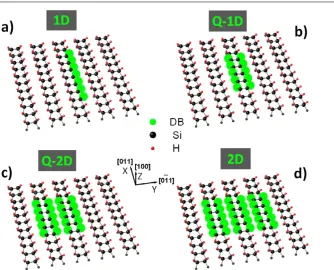
Figure 1 shows schematically the different DB nanowires on the hydrogen passivated Si(100)-(2×1) surface that are considered in the present work. The clean Si(100) surface (2×1)-reconstruction involves the formation of parallel dimer rows with a single dangling bond associated with each surface atom, which can in turn be passivated with hydrogen atoms (red circles in figure1). The four wire configurations shown in figure 1 were fabricated by hydrogen desorption using the STM probe [1,2]. The bright green circles correspond to the DBs and for clarity in each case the partially or fully bare dimers are depicted as being symmetric even though they are buckled. We refer to the fabricated DB wires as being 1D, 2D, quasi Q-1D or Q-2D. In all cases the electronic properties of these wires were investigated by scanning tunneling spectroscopy (STS) and LDOS maps [14] were constructed along the principle directions of these wires. In all spectroscopic data presented here the surface and probe combined local density of states (LDOSs,t)was recovered [15] from the simultaneously measured dI/dV(V) and I(V) spectra. The use of the combined LDOS for the surface characterization is a good approximation to the actual surface density of states since the electronic structure of the metallic tip is larger in magnitude and less corrugated in comparison with that of semiconductor surface [17]. Moreover, even if the probe LDOS becomes corrugated due to uncontrolled hydrogen adsorption, it was demonstrated previously [17] that this will only significantly impact the filled states bias region below−1 V. We will now provide a detailed description of the four types of DBs wires shown in figure1.
3.1. 1D wire
One-dimensional (1D) wires were fabricated by removing single H atoms from each dimer along the same side of the dimer row as shown in figure 1(a). Although this DB configuration is energetically unfavorable [18] it is possible to fabricate [3] such wires by STM. Since these wires are nominally comprised of half-filled orbitals, early theoretical predictions [5] indicated that the wires are metallic with the Fermi level located at the DB energy. However, high resolution topographic images [3] demonstrated periodic corrugation along the wire length that is dependent on the number of DBs that comprise the wire, which has been interpreted in terms of a Jahn–Teller distortion. But
such distortions are expected to lead not only to charge redistribution along the wire but also to open up a band gap at the Fermi level. Unfortunately there was no spectroscopic characterization of the excellently resolved wires reported in [3] and so it was not possible to confirm the existence of a band gap induced by the Jahn–Teller distortion or indeed the lack of a band gap predicted [5] for infinite non-distorted wires. To the best of our knowledge there are no STS data for isolated 1D DB nanowires published in the literature to date. The spectroscopic data presented in [4] were measured on wires composed of mixtures of single dangling bonds and bare dimers and were metallic in nature.
Recent spin-polarized density-functional theory calcula-tions [12] compared charge ordering due to Jahn–Teller dis-tortion with re-ordering due to antiferromagnetic alignment of the spins of adjacent DBs. It was found that antiferromagnetic alignment produces a significant band gap (from 0.9 to 0.6 eV) for wires with even and odd number of DBs in contrast to the nonmagnetic order where gap was found only for even numbers of DBs.
Our results for STM-fabricated 1D DB-wire are presented in figure 2. The wire is comprised of an odd (7) number of DBs (see figure 1(a)), determined by confirming the registry with respect to the lattice corrugation of the surrounding hydrogen passivated surface. In the topographic cross section shown in figure2(b) (position shown with arrow in figure 2(a)) it can be seen that we do not detect a strong topographic height modulation similar to that reported in [3]. Because our sample and imaging conditions correspond to those in [3], the most likely reason for the weaker modulation observed here is due to the difference in the STM tip–apex sharpness and composition. In our case the transfer of Pt metal to the tip during the inking process, which is essential to insure that the tip remains metallic during spectroscopic measurements, does not lead to an exceptionally sharp tip. In contrast, etched tungsten tips that exhibit good resolution when imaging Si surfaces are typically covered with Si atoms but provide unreliable spectroscopic data. Despite this we still can observe a maximum in the middle of the wire (see topographic cross section in figure 2(b)) which is consistent with the results for odd number of DBs found in the high resolution images in [3].
In order to spatially characterize the electronic structure of the DB-wire we measured multiple spectra along the middle of the wire (see arrow in figure 2(a) and dots in figure 2(b)). The combined tip and sample local density of states (LDOSs,t)was recovered [15] from the experimental spectra and plotted as a color map in figure2(c). The LDOSs,t map in figure 2(c) shows almost featureless electronic structure of the 1D nanowire along its entire length (abscise in figures 2(b) and (c)) apart from the modulation around
+1.3 V, which is likely associated with the reorganization of the back bond charges [19] and is the source of the weak corrugation observed in the topography (see figure 2(b)). Figure 2(c) shows a symmetric band gap with an energy width of roughly 0.8 eV. The existence of a band gap in the experimental electronic structure for the finite odd (7 DBs) wire in figure 2(c) strongly supports the model of
Figure 1. Schematics of the hydrogen passivated Si(100)-(2×1) surface with dangling bond (DB) nanowires in green. (a) Line of single dangling bonds, (b) row of bare silicon dimers, (c) two adjacent bare-dimer rows, and (d) three adjacent bare-dimer rows. The structure dimensionalities are marked in the corresponding gray boxes and the assignments are discussed in the text. The atoms in all panels of the figure are with the same color coding as indicated in the middle of the figure.
Figure 2. 1D nanowire formed by a line of 7 single dangling bonds (schematics in figure1(a)) on hydrogen passivated Si(100)-(2×1) surface. (a) Topographic image of the nanowire taken with sample bias of 2.0 V and tunneling current of 25 pA. (b) Topographic line measured along the wire and indicated in (a) with an arrow. (c) Spatial LDOSs,tmap composed of individual (dots in (b)) spectra measured along the line in (b). All panel abscissas are with the same scale and are aligned.
antiferromagnetic ordering proposed in [12], and in particular is inconsistent with the Jahn–Teller distortion model that predicts a gap only in the case of even numbers of DBs. The antiferromagnetic model [12] also predicts no corrugation of
the DB-wire along its length which is consistent with our topographic results (see figures2(a) and (b)).
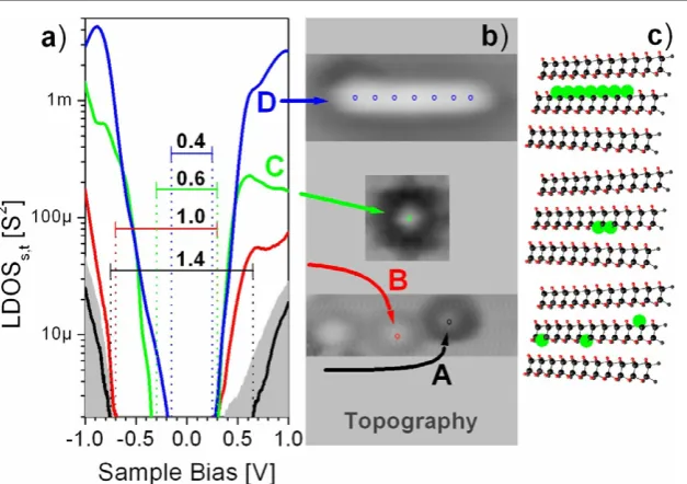
To better understand the origin of the band gap behavior for the 1D wire, the spectra of isolated and coupled dangling bonds on a passivated n-type Si(100) surface were recorded (see figure3(a)). The appearance of individual DBs depends on their location and in particular their proximity to other DBs, and is illustrated by the topographic images of DBs labeled A and B, in the bottom panel of figure 3(b). This behavior is a consequence of the interaction between DBs and tunnel coupling between sites that changes the local charge occupancy [20]. Various levels of charging (between 1 and 2 electrons per DB [20]) are responsible for the different appearance of the DBs in topographic images. In the case of figure3(b), dangling bond A is doubly occupied [20] with a filled DB stated below−1 V (black spectrum in figure3(a)) whereas dangling bond B is not fully occupied as evidenced by the significant empty DB feature at 0.65 V (red curve in figure3(a)). The local band gap at the A is 1.4 V consistent with the 1.5 V gap found for an isolated DB in [9], whereas the less occupied dangling bond B has a reduced gap of approximately 1.0 V.
[image:4.595.53.289.406.598.2]Nanotechnology24(2013) 275202 B Naydenov and J J Boland
Figure 3. Band gap variation for separated and adjacent single dangling bonds. (a) LDOSs,tspectra of two separated (A) (black) and (B) (red), two adjacent (C) (green), and seven adjacent (D) (blue) dangling bonds (ordinate in logarithmic scale). The corresponding band gap values are indicated in Volts. The gray filled area is the LDOSs,tof the hydrogen passivated Si(100)-(2×1) surface. (b) Topographic images with the same conditions as in figure2are marking (color coded small circles) the location of the (a)-spectra acquisition. (c) Schematics of the structures presented in (b) using the same color coding as the schematics in figure1.
singly occupied dangling bond B (red curve in figure 3(a)). The observed band gap in this case is in between the values calculated in [12], 0.45 eV for the nonmagnetic and 0.89 eV for the antiferromagnetic case.
The blue spectrum in figure 3(a) is an average of the spectra measured along the length of the wire in figure2and shows that the band gap estimated to be 0.8 V from figure2(c) is actually 0.4 V when the logarithmic decay of the density of states into the gap is fully accounted for as shown in LDOS curve D in figure3(a). Note this energy gap value of 0.4 V is significantly different from the 0.66 V value calculated in [12]. This correction is due to the presence of a small tail extended from the filled states into the band gap. Thus the disagreement with the theory [12] could be due to the zero-temperature calculations compared to the 77 K of our experiment or could also be due to tip effects not considered in the theory.
3.2. Q-1D wires
A wire comprised of an array of bare dimers along a single row (figure1(b)) is expected to behave like the clean Si(100)-c(4 × 2) surface [14] in that the dimer tilting is anticorrelated along the length of the wire. This assumption was confirmed by topographic images presented in [4]. In the same study [4] the normalized conductance spectrum was shown averaged along a bare-dimer wire which was part of longer wire that also contained single DB (i.e. 1D wire sections, see figure 1(a)) as well. The results in [4] demonstrated a band gap of 0.5 eV which was significantly smaller than the 1.0 eV value reported previously [21] for isolated bare dimer on passivated Si(100)-(2×1).
Here we fabricated (see section 2) and characterized isolated bare-dimer wires (see figure1(b)) of different lengths.
The results for three wires with lengths of 2 nm, 3.6 nm, and 6.2 nm are presented in figures 4(a)–(c), respectively. The data were acquired using the same procedure as those in section 3.1 and are presented in the same manner as that in figure 2. In contrast to the topographic image in figure 2(a) all images in the top panels of figure 4 show the presence of two ridges that run along the wire length, consistent with the wire being comprised of bare dimers, each with two DBs. The blue arrows in these panels point along the minimum between these ridges, i.e. along the middle of the dimer row. On the reconstructed clean Si(100)-c(4×2) surface the dangling bonds of the dimers are known to react with each other and to form bonding π and antibonding π∗ bands separated by 0.6 eV [15]. Although the surface
states have two-dimensional (2D) periodicity the dispersion of the π∗ band is strong only [9] along the dimer-row direction making it quasi-one-dimensional (Q-1D) band with observable quantum scattering [14,22,23] and confinement effects [24,25]. As the [011] direction is also along the dimer direction, and thus along the wire length, the absence of appreciable interaction in the perpendicular direction suggests that we can assign the bare-dimer wires in figure 4 as quasi-one-dimensional (Q-1D) systems. This assignment is strongly supported by the appearance of quantum confinement in the isolated wires, which is most obvious in the LDOSs,t map in figure 4(c). The π∗ band on heavily doped n-type Si(100) surface occupies the positive sample bias range from 0 to 0.6 V [25] and this is exactly the range in which energy quantization is observed in the quantum wells formed in these wires (see figure4).
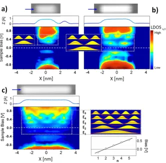
The bottom panel of figure 4(c) shows clear evidence of a quantum well with quantized states at E1 = −0.18 V, E2=0.05 V,E3=0.24 V,E4=0.42 V, andE5=0.57 V,
Figure 4. Nanowires composed of a bare silicon dimer row (schematics in figure1(b)) with different lengths. The various panel-group contents (a)–(c) follow the manner of figure2. (a) Panel-group represents the data for a nanowire with length approximatelyL∼2 nm (5 bare dimers), (b) corresponds toL∼3.6 nm (10 bare dimers), and (c) toL∼6.2 nm (17 bare dimers). The topographic imaging conditions are as in figure2. All panels are vertically aligned. The same scales are preserved for all figures2–4. Corresponding illustrative schematics of the standing waves (red curves) and the probability measured by STS (yellow filled peaks) are inserted in (a) and (b) and positioned on the right-hand side of (c). The dispersion of the discrete states is presented in the bottom right of (c). The quantum well in (a) appears tilted due to the influence of an isolated dangling bond along the same dimer row (see middle panel in (a)).
that exhibit zero—four nodes in the LDOS respectively. This is illustrated schematically by the standing waves (red curves) and the probability or LDOS measured by the tunneling spectroscopy (yellow filled peaks) on the right-hand side of figure 4(c). The energy dispersion is plotted in the bottom-right side of figure4(c) and is approximately linear, indicating that the well shape is parabolic rather than a square well. For the shorter wire in figure 4(b) two well resolved levels are observed at E2 =0.18 V and E3=0.49 V. The first level (n = 1) is most likely at the Fermi level (see schematics in figure4(b)) but is split and reduced by Coulomb repulsion and is not detected in figure 4(b). The structure around−0.25 V deviates too much in energy from the linear dispersion found in the longer wire in figure 4(c) and thus is probably not related to theπ∗band but rather to the band around −0.45 V observed in figure4(c) and at−0.15 V in figure 4(a). However, at this juncture it is not possible to definitively assign this feature without detailed computational modeling.
Since the wire in figure4(b) is shorter than the wire in figure4(c), as expected the discrete levels are shifted to higher energy and there is an increase in the energy level separation. The quantum well levels continue to shift towards higher
energies with further shortening of the wire and in figure4(a) (the shortest wire) the first discrete energy is resolved at E1=0.25 V and a gap is seen to open up at the Fermi energy. It is interesting to note that the band gap at the Fermi level has been previously reported to be 1.0 V [21] for the case of an isolated bare dimer on a hydrogen passivated Si(100)-(2×1), but based on the results here the gap decreases as the length of the Q-1D wire increases. For instance in the 2 nm long wire (see figure4(a)) the gap is reduced to 0.25 V. The 3.6 nm Q-1D wire (see figure4(b)) has a small 0.1 eV bang gap but it is asymmetric and mostly located in the negative bias range. However, the 6.2 nm Q-1D wire (see figure4(c)) has no band gap. The first quantum well level is filled, the Fermi level is at the second discrete level, and the wire has a metallic character.
3.3. Q-2D and 2D wires
Nanotechnology24(2013) 275202 B Naydenov and J J Boland
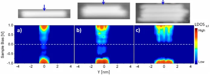
Figure 5. Nanowire composed of single and multiple adjacent bare-dimer rows. The vertical panel-group contents follow the manner of figures2and4. (a) Repeats figure4(c) for better comparison with the data in (b) and (c). (b) Two adjacent bare-dimer rows (schematics in figure1(c)). (c) Three adjacent bare-dimer rows (schematics in figure1(d)). All spectra were taken along the rows (17 bare dimers) indicated with blue arrows. The topographic imaging conditions are as in figures2–4. All panels are vertically and horizontally aligned. The same scales are preserved from figure4. The red dashed line follows the shift of the quantized discrete level withn=3.
Figure 6. Cross-section electronic structure of single and multiple dimer-rows nanowires presented in (a)–(c) correspond to the wires in figures5(a)–(c), respectively. The arrows indicate the location of the corresponding STS-set of measurements.
in figure5(a). From the LDOSs,t maps in figure5it is clear (red dashed line) that the quantum well states undergo a blue shift as the number of adjacent bare-dimer rows is increased. As the wire length is almost unchanged this continuous shift can be related only to the increased coupling between the bare-dimer wires. Thus although the dispersion is weak in this perpendicular direction it is critical in controlling the band gap and indeed the properties of the pristine clean surface. This can be seen by noticing that in addition to the shift of π∗band to higher energies the band gap gradually opens with
the addition of rows such that even for the three wire case in figure5(c) the gap is around 0.6 V, which is similar to that observed on a clean n-type Si(100) surface [15]. Based on this we assign the triple DB-wire as a two-dimensional (2D) semiconductor nanowire.
The double nanowire in figure 5(b) has an electronic structure significantly altered when compared to the single-row wire in figure5(a) yet still has a metallic character with broad feature in the band gap region of the clean surface. This wire has an intermediate character between the Q-1D (see figure5(a)) and the 2D (see figure 5(c)) nanowires and could be assigned as quasi-two-dimensional (Q-2D) wire. Although the wire exhibits coupling in the second dimension, the coupling is not strong enough to reproduce the clean
surface electronic structure so that the wire still retains with metallic character.
We can further study this lateral coupling by examining the LDOS in the direction perpendicular to the wires in figure 5. These lateral LDOSs,t maps measured across (Y-direction, see figure 1) are presented in figure 6. The maps were constructed from spectra taken across the middle of the wires as indicated by arrows in figure 6. Despite the slight variation of the tip sharpness (compare the topographic images in figure 6) due to the wire fabrication process it is obvious that the surface states are localized on the dimer rows for all the three wire assembled in figure6. This indicates that the energy shifts observed in figures5and6could be due to Coulomb repulsion between the wires.
4. Summary
We have fabricated and characterized various dangling bond (DB) nanowires on a passivated n-type Si(100)-(2 × 1) surface. The nanostructures were fabricated using the STM tip [1,2] and were characterized by variable-height scanning tunneling spectroscopy [15] which allows for spatially resolved electronic structure determination (see figures 2, 4–6). The combined tip and surface local density of states (LDOSs,t)of the nanostructures with various dimensionality
[image:7.595.125.475.285.410.2]Figure 7. LDOSs,tspectra averaged along the corresponding nanowire lengths. The spectra are plotted with the area beneath curves filled in black. The band gap when present is marked with red box. On the right-hand side of each panel the corresponding assigned dimensionality and length are indicated. All panels are with the same scale and are vertically aligned. (a) Averaged spectrum of the DB-line in figure2(schematics in figure1(a)). (b)–(d) Averaged spectra of the nanowires in figures4(a)–(c), respectively. (e) and (f) are averaged spectra of the double and triple wire from figures4(b) and (c). The red dashed line follows the shift of the quantized discrete level withn=3.
are summarized in figure 7 in which the spectra have been averaged along the wire lengths. We observed a significant band gap at the Fermi level for 1D nanowire (see figure7(a)). The gap is present for Q-1D wires shorter than 4 nm but vanished for wires above 4 nm (see figures 7(b)–(d)). Populating one sides of a Q-1D nanowire with bare-dimer row of the same length reduces the amplitude and smears the electronic states in the Si bulk band gap of the still metallic wire (see figure 7(e)). While populating both sides of the Q-1D wire with DBs completely converts the metallic wire into a semiconductor (see figure7(f)) with an electronic structure that is similar to the bare Si(100) surface with n-type doping.
In conclusion we have demonstrated experimentally that by changing only the size and dimensionality of surface nanowires on semiconductor sample it is possible to alter their character from semiconductive to metallic and vice versa. Although this example is not directly applicable for device fabrication it is very instructive and may provide a route to fabricating device component without the need to add new materials or to increase the system complexity.
Acknowledgments
This work was supported by Science Foundation Ireland under PI Award Grant No. 06/IN.1/I106 and CRANN.
The authors would like to thank Dr I Rungger, Dr M Mantega, and Professor S Sanvito for their stimulating discussions.
References
[1] Shen T C, Wang C, Abeln G C, Tucker J R, Lyding J W, Avouris P and Walkup R E 1995Science2681590 [2] Lyding J W, Shen T C, Hubacek J S, Tucker J R and
Abeln G C 1994Appl. Phys. Lett.642010
[3] Hitosugi T, Heike S, Onogi T, Hashizume T, Watanade S, Li Z Q, Ohno K, Kawazoi Y, Hasegawa T and Kitazawa K 1999Phys. Rev. Lett.824034
[4] Hitosugi T, Hashizume T, Heike S, Wada Y, Watanabe S, Hasegawa T and Kitazawa K 1998Appl. Phys.A66S695 Hitosugi T, Hashizume T, Heike S, Kajiyama H, Wada Y,
Watanabe S, Hasegawa T and Kitazawa K 1998Appl, Surf. Sci.130–132340
[5] Watanabe S, Ono Y A, Hashizume T and Wada Y 1996Phys. Rev.B54R17308
[6] Doumergue P, Pizzagali L, Joachim C, Altibelli A and Baratoff A 1999Phys. Rev.B5915910
[7] Soukiassian L, Mayne A J, Carbone M and Dujardin G 2003 Surf. Sci.528121
[8] Tong X and Wolkow R A 2006Surf. Sci.600L199 [9] Bellec A, Riedel D, Dujardin G, Boudrioua O, Chaput L,
Stauffer L and Sonnet P 2009Phys. Rev.B80245434 [10] Weber Bet al2012Science33564
[11] Bird C F and Bowler C F 2003Surf. Sci.531L351
[12] Lee J Y, Cho J H and Zhang Z 2009Phys. Rev.B80155329 [13] Chadi D J 1979Phys. Rev. Lett.4343
[14] Naydenov B, Mantega M, Rungger I, Sanvito S and Boland J J 2011Phys. Rev.B84195321
[15] Naydenov B and Boland J J 2010Phys. Rev.B82245411 [16] Naydenov B, Ryan P, Teague L C and Boland J J 2006Phys.
Rev. Lett.97098304
[17] Pfeifer H, Koslowski B and Ziemann P 2011Beilstein J. Nanotechnol.2607 and all cited therein
[18] Boland J J 1991Phys. Rev. Lett.671539
[19] Perdig˜ao L, Deresmes D, Grandidier B, Dubois M, Delerue C, Allan G and Sti´evenard D 2004Phys. Rev. Lett.92216101 Dubois M, Perdigao L, Delerue C, Allan G, Grandidier B,
Deresmes D and Sti´evenard D 2005Phys. Rev.B71165322 [20] Haider M B, Pitters J L, DiLabio G A, Livadaru L, Mutus J Y
and Wolkow R A 2009Phys. Rev. Lett.102046805 [21] Chen D and Boland J J 2002Phys. Rev.B65165336 [22] Yokoyama T, Okamoto M and Takayanagi K 1998Phys. Rev.
Lett.813423
[23] Sagisaka K and Fujita D 2005Phys. Rev.B72235327 [24] Yokoyama T and Takayanagi K 1999Phys. Rev.B5912232 [25] Sagisaka K and Fujita D 2006Appl. Phys. Lett.88203118