IMC Growth of Solid State Reaction between Ni UBM and Sn–3Ag–0.5Cu
and Sn–3.5Ag Solder Bump Using Ball Place Bumping Method during Aging
Shinji Ishikawa
1;*, Eiji Hashino
1, Taro Kono
2and Kohei Tatsumi
11
Advanced Technology Research Laboratories, Nippon Steel Corp., Futtsu, 293-8511, Japan 2New Materials Division Nippon Steel Corp., Tokyo, 100-8071, Japan
The bumps for flip chip interconnection are becoming smaller and smaller. Since lead-free solders became popular, Ni-based under bump metallization (UBM) has attracted attention in recent years because of their slower reaction rate than traditional Cu-based UBM. However, there is little data concerning the solid state reaction between small lead-free solder bumps and Ni-based UBM. In this work, Sn–3Ag–0.5Cu and Sn–
3.5Ag solder bumps were fabricated with 110-mm-diameter solder balls on electrolytic Ni, and the growth kinetics of intermetallic compound
(IMC) layers and the morphology of bumps during long-term aging were investigated. The IMC layer exhibited parabolic growth, and the activation energy values for the Sn–3Ag–0.5Cu or Sn–3.5Ag solder/Ni UBM were obtained. The growth rate accelerated at 463 K or above.
(Ni,Cu)3Sn4or Ni3Sn4IMC was formed mainly at the solder/Ni interface after long-term aging. Large voids were formed at the solder/IMC
interface at 463 K or above. The voids are the result of stress by volume expansion due to IMC growth. Coarse Ag3Sn grains were observed adjacent to the voids and contributed to void initiation.
(Received May 19, 2005; Accepted October 4, 2005; Published November 15, 2005)
Keywords: solder, lead-free, electrolytic nickel, flip chip, intermetallic compound, isothermal aging, microstructure, growth kinetics
1. Introduction
With progress in high-density, high-speed technologies for semiconductor devices in recent years, high performance and substantial downsizing of electronic equipment have been achieved. These advancements in LSI technology has led to an increase in the number of input and output pins and a decrease in the size and pitch of electrodes. With this situation, some chip interconnection technologies using bonding wires are being replaced by flip chip interconnection technologies, where bumps are formed on chip electrodes and the chips are bondedviathese bumps. In advanced areas of flip chip interconnection, ultra fine pitches and minimized bumps are required to meet the demand for higher density packages. On the other hand, using lead-free solders for flip chip interconnection instead of traditional eutectic Sn–Pb solders in electronics has increased from the viewpoint of environmental-friendly technology.1)Therefore, in flip chip technologies, both fine pitch interconnection and lead-free solder are to be developed simultaneously.
Since the introduction of flip chip technology by IBM in the 1960s, under bump metallization (UBM) has become essential in solder bumps.2)As lead-free solders have become
popular in recent years, Ni-based UBM has attracted attention because of their slower reaction rate than traditional Cu-based UBM. Many studies have been devoted to under-standing the interactions between Sn-rich solders and Ni-based UBMs. While many studies on the intermetallic compounds (IMCs) formed as a result of interfacial reactions between Sn–Ag–Cu solders and different Ni-based UBMs, such as Cu/Ni/Au,3–5) Al/Ni(V)/Cu6,7) and Ni(P)/Au8–12)
have been reported, there have been few studies on the IMCs formed between Sn–Ag–Cu solders and pure Ni UBM without an Au protective barrier. Furthermore, data on solid state reactions between especially small lead-free solder
bump and pure Ni UBM are not sufficient. It is expected that with a different volume of bumps, their morphology and their growth rate under thermal aging conditions change.
Currently, ultra fine pitch bumps, under 200mm for flip chip interconnection, are fabricated mainly using the electro-plating solder bump method. In this method, it is difficult to form bumps of ternary or more solder composition. This may be one reason that we do not have sufficient data for the ultra fine pitch bumps of lead-free solder, such as the Sn–Ag–Cu ternary system. However, a new ball-place-bumping method has been developed by the authors.13) This technique
industrially achieved fine pitch bumping and a decrease in the limitation concerning the solder composition of bumps. With this method, solders for flip chip interconnection will change to ternary or more systems because of beneficial properties such as thermal fatigue.14)
This paper compares interaction between three solder bumps (Sn–3Ag–0.5Cu, Sn–3.5Ag and for comparison, Sn– 37Pb) fabricated using the ball-place-bumping method and electrolytic Ni UBM. The morphology of IMC formed under reflow and thermal aging conditions was observed. IMC growth kinetics was assessed and compared for the three systems. This comparison among the three solder/UBM combinations will aid an understanding of the effects of solder composition and UBM composition on the interfacial reaction.
2. Experimental
The Si substrates used in this study were electrolytic Ni UBMs with 110-mmdiameter and 5-mmthickness formed on a Si wafer fabricated by a commercial organization. To obtain basic data, UBM composed of only Ni without any surface protective metals such as Au was used. The bumps were formed on the UBM using the ball-placing method as shown in Fig. 1(a). The diameter of the solder ball used was 110mm. After the UBMs were cleaned with 0.1 N HCl
*E-mail: [email protected]
Special Issue on Lead-Free Soldering in Electronics III
solution for 300 s, Sn–3Ag–0.5Cu, Sn–3.5Ag and Sn–37Pb solder balls were placed on the UBM with RMA-type flux. They were then subjected to reflow treatment twice with a peak temperature of 533 K to fit the initial conditions of common flip chip bonding. The temperature profile of the reflow is shown in Fig. 2.
The samples were isothermally aged at 398, 423, 448, 463 and 473 K for 0:18106s, 0:72106s, 1:8106s, 3:6 106s and 7:2106s. After each of the aging steps, the
samples were mounted in epoxy and metallographically polished for micro-structural characterization. Micro-struc-tural and chemical analyses of the samples were conducted using an optical microscope, a scanning electron microscope (SEM) and an electron probe micro analyzer (EPMA). The layer thickness was measured using image analysis software to obtain the total area of the intermetallic layer.
3. Results and Discussion
3.1 Morphology of IMC
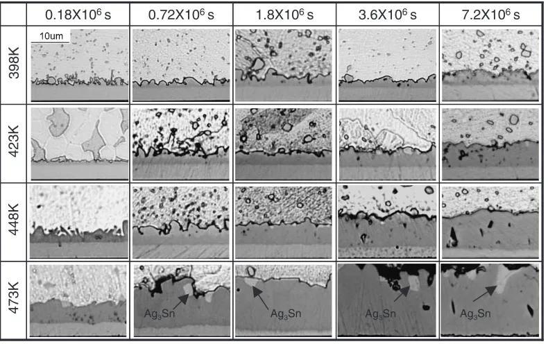
Typical cross-sectional views of the interfacial micro-structure of the three solder/UMB systems (Sn–3Ag–0.5Cu,
Sn–3.5Ag and Sn–37Pb solder with electrolytic Ni UBM) after aging up to7:2106s at 398, 423, 448, and 473 K are
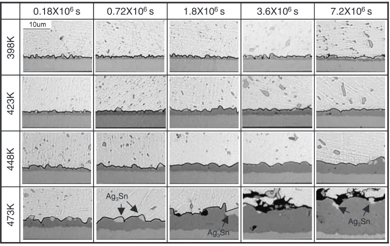
shown in Figs. 3–5. The IMC layer in the Sn–3Ag–0.5Cu solder/electrolytic Ni UBM system had chunky, needle-like, grains at the initial state. The IMC layer in the Sn–3.5Ag and Sn–37Pb solder/electrolytic Ni UBM system had smoother contour lines. This morphology is in agreement with previous reports on a Cu/Ni/Au BGA pad obtained in the Sn–3Ag– 0.5Cu and Sn–3.5Ag solder systems4)and sputtered Ni/Au
UBM in the Sn–3.5Ag and Sn–37Pb solder systems.10)The
IMCs of the three systems evolved over all aging conditions were studied. However, Ni UBM was fully consumed at 473 K after aging for7:2106s in the Sn–3Ag–0.5Cu solder
Flux
After Reflowed Solder Ball
Ball Placed Ni UBM
Si
(a) (b)
Fig. 1 Schematic illustration of bump formation.
Fig. 2 Temperature profile of the reflow treatment.
7.2X10⁶s 3.6X10⁶s
1.8X10⁶s 0.72X10⁶ s
0.18X10⁶ s
398K
448K
423K
473K Ag
3Sn
Ag3Sn Ag3Sn Ag3Sn
[image:2.595.54.284.69.202.2] [image:2.595.309.541.72.296.2] [image:2.595.102.497.521.769.2]system. The contour lines of IMC of Sn–3Ag–0.5Cu gradually became smooth after long-term aging. The growth rate of IMC was most rapid in the order of Sn–3Ag–0.5Cu, Sn–37Pb, and Sn–3.5Ag. This is consistent with the research by Sharif et al. on Ni/Au UMB/Sn–3Ag–0.5Cu and Sn– 3.5Ag solder systems.4)While Sharifet al.also reported that
the entire 5-mmNi layer was consumed from the substrate pads after aging for1:4106s at 463 K, in the present work,
full consumption required7:2106s at 473 K. This
differ-ence is due to the infludiffer-ence of the ball diameter used, that is, the diameter of the solder ball used by Sharifet al.of 760mm
was much larger than that of this work (110mm). Meanwhile, Heet al.reported that IMC in the sputtered Ni/Au UBM/Sn– 3.5Ag solder system showed more rapid growth than the sputtered Ni/Au UBM/Sn–37Pb solder system.10) This difference is attributed to the existence of Au, because, in their system, a layer of Au–Ni–Sn ternary IMC was formed
on the top of the Ni–Cu–Sn IMC layer and must have suppressed the growth of IMC.
When aged at 473 K, large voids were formed in the Sn– 3Ag–0.5Cu solder after 0:72106s and in the Sn–3.5Ag
solder after 1:8106s as shown in Figs. 3 and 4,
respec-tively. The thickness of IMC at these times was larger than 10mm. In the case of Sn–37Pb solder, such voids were not observed despite the formation of about 10-mmthick IMC. Such voids have not been previously reported in much research on Ni-based UMB/high Sn solder joints, and were first observed in this work. The reason that has it not been reported up to now is that the volume of the bumps is especially small in this work. In addition, in the solders, Sn– 3Ag–0.5Cu and Sn–3.5Ag, where voids were formed after long-term aging at 473 K, large Ag3Sn particles, shown in
Figs. 3–4, were observed at the boundary region between the solder and IMC.
6 3.6X10⁶s 7.2X10⁶s
1.8X10 s 0.72X10⁶ s
0.18X10⁶ s
398K
448K
423K
Fig. 5 Optical microscope image of Sn–37Pb solder/electrolytic Ni joints after aging for up to7:2106s from 398 to 448 K.
7.2X10⁶s 3.6X10⁶s
1.8X10⁶s 0.72X10⁶ s
0.18X10⁶ s
398K
448K
423K
473K
Ag3Sn
Ag3Sn Ag3Sn
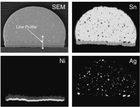
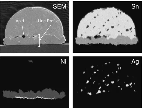
[image:3.595.101.495.72.321.2] [image:3.595.104.492.355.544.2]The EPMA analysis results of as-reflowed and aged Sn– 3Ag–0.5Cu and Sn–3.5Ag solders joints for 1:8106s at
423 K are shown in Figs. 6–11. The IMCs formed between the Sn–3Ag–0.5Cu solder and electrolytic Ni were Ni–Cu–Sn ternary IMC, while those of the Sn–3.5Ag solder and Sn– 37Pb were Ni–Sn binary IMC. Neither Ag of Sn–3Ag–0.5Cu and Sn–3.5Ag solder nor Pb of Sn–37Pb solder was involved in interfacial reactions. In this study, EPMA quantitative analysis confirmed that IMC formed at the interface of the sample after long-term aging is (Ni,Cu)3Sn4or Ni3Sn4. The
composition of Cu in (Ni,Cu)3Sn4 in the Sn–3Ag–0.5Cu
solder was 5.3 mass% Cu at 423 K and 2.5 mass% Cu at 473 K. Since the amount of Cu was limited in the solder and
Sn
Ag
Ni
SEM
Cu
Sn
Ag
Ni
SEM
Cu
5µµm
Fig. 6 SEM image and EPMA mapping of Sn–3Ag–0.5Cu
solder/electro-lytic Ni joints as-reflowed.
SEM
Sn
Ag
Ni
5µµm
Fig. 7 SEM image and EPMA mapping of Sn–3.5Ag solder/electrolytic
Ni joints as-reflowed.
SEM Sn
Ag Ni
Line Profile
Fig. 8 Whole bump EPMA mapping of Sn–3Ag–0.5Cu solder/electrolytic
Ni joints after aging for7:2106s at 423 K.
SEM Sn
Ag Ni
Line Profile Void
Fig. 9 Whole bump EPMA mapping of Sn–3Ag–0.5Cu solder/electrolytic
Ni joints after aging for7:2106s at 473 K.
SEM Sn
Ag Ni
[image:4.595.54.284.69.333.2]Line Profile
Fig. 10 Whole bump EPMA mapping of Sn–3.5Ag solder/electrolytic Ni
[image:4.595.309.543.71.250.2] [image:4.595.310.544.324.502.2] [image:4.595.55.284.396.566.2] [image:4.595.309.545.578.757.2]the volume of IMC at 473 K was larger than at 423 K, the Cu content at 473 K was smaller than at 423 K. The quantitative results of EPMA analysis for the IMCs formed at the interface in this study are shown in Table 1 and Figs. 12–13. Previous results showed that the IMCs formed at the interface of Sn–Ag–Cu solder and pure Ni depended on the Cu concentration in the solder material. Zenget al.6)pointed
out that the formation of (Cu,Ni)6Sn5 dominated at the
SEM Sn
Ag Ni
[image:5.595.52.285.72.249.2]Line Profile Void
Fig. 11 Whole bump EPMA mapping of Sn–3.5Ag solder/electrolytic Ni
[image:5.595.110.490.325.523.2]joints after aging for7:2106s at 473 K.
Table 1 EPMA composition analysis results of IMCs formed at the Sn–
Ag–Cu/Ni interface.
(mass%)
Solder Aging
Temp. Sn Ni Cu C
Sn–3Ag–0.5Cu 423 K 66.0 27.5 5.3 Bal.
473 K 64.3 31.7 2.5 Bal.
Sn–3.5Ag 423 K 65.8 32.5 — Bal.
473 K 66.4 30.0 — Bal.
0 200 400 600 800
0 50 100 150 200 0
300 600 900
0 200 400 600
(a)
(b)
IMC IMC
Sn
Ni
Cu
Sn
Ni
Cu Ag3Sn
5µm
Distance, d/µm Distance, d/µm
Intensity, /(abs. unit) Intensity, /(abs. unit)
Fig. 12 Line profile of EPMA mapping of Sn–3Ag–0.5Cu solder/electrolytic Ni joints after aging for7:2106s (a) at 423 K and (b) at
473 K.
0 200 400 600 800
0 100 200 300 400 500 0
300 600 900
0 200 400 600
(a)
(b)
Distance, d/µm
IMC IMC
Distance, d/µm Sn
Ni
Sn
Ni 5µm
Intensity, /(abs. unit) Intensity, /(abs. unit)
[image:5.595.110.489.571.767.2]interface when the Cu concentration in the solder was more than 0.6 mass%. In addition, when the Cu concentration in the solder was so small, (Ni,Cu)3Sn4 was formed at the
interface. In fact, in the Sn–0.2 mass%Cu solder, the product of the solder reaction with Ni was (Ni,Cu)3Sn4, and in the
Sn–0.7 mass%Cu solder, the product of the solder reaction with Ni was (Cu,Ni)6Sn5.15) Further, in the Sn–3.8
mass%Ag–0.7 mass%Cu solder, (Cu,Ni)6Sn5 was formed at
the interface.12)The morphology change in Sn–3Ag–0.5Cu
solder in Fig. 3 and the quantitative analysis results in Table 1 were in agreement with these results. Since a small amount of Cu exists, the IMC formed first is considered to be (Cu,Ni)6Sn5 that has chunky, needle-like grains.7) After
prolonged aging, however, the lack of Cu lead to the formation of a continuous (Ni,Cu)3Sn4 layer. On the other
hand, IMCs formed by the reaction between Sn–3.5Ag solder or Sn–37Pb solder and electrolytic Ni UBM were continual Ni3Sn4because of the lack of Cu.
In this work, Ag3Sn was observed in the form of small
particles distributed in the body of the solder bumps at the initial state. In addition, Ag3Sn grains obviously become
larger by coalescence with the progress of aging in Figs. 8– 11. There was no large branch-like or plate-like phase, even in high-temperature, long-term aging for 7:2106s at
473 K.
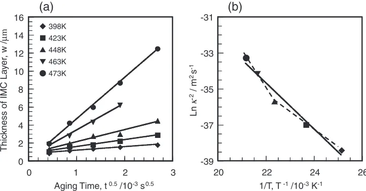
3.2 Growth kinetics of IMC
The thickness of (Ni,Cu)3Sn4or Ni3Sn4 IMC in the three
solder/UBM systems is shown as the function of aging time and temperature in Figs. 14(a)–16(a). The thickness of IMC increased linearly with the square root of the aging time at each aging temperature. This indicates that the IMC growth in all the systems studied is a diffusion-controlled process. The growth rate constant at a particular temperature,k, can be calculated from the slope of the linear fitting lines. The temperature dependence of k can be represented by the Arrhenius equation:
(b)
Aging Time, t0.5/10-3s0.5
Thickness of IMC Layer, w /
µ m
(a)
Ln κ 2 / m 2s -11/T, T-1/10-3K-1
0 2 4 6 8 10 12 14 16
0 1 2 3
398K 423K 448K 463K 473K [ [ [ [ [ [ -39 -37 -35 -33 -31
[image:6.595.115.482.74.264.2]20 22 24 26
Fig. 14 (a) Average thickness of the IMC layer of Sn–3Ag–0.5Cu solder/electrolytic Ni joints with aging time and temperature and
(b) Arrhenius plot for the growth of the IMC layer.
-39 -37 -35 -33 -31 22
20 24 26
0 2 4 6 8 10 12 14 16
0 1 2 3
(a)
(b)
Aging Time, t0.5/10-3s0.5
Thic
kness of IMC La
y e r, w / µ m Ln κ 2 / m 2s -1
1/T, T-1/10-3K-1
398K
423K
448K
463K
473K
Fig. 15 (a) Average thickness of the IMC layer of Sn–3.5Ag solder/electrolytic Ni joints with aging time and temperature and
[image:6.595.117.478.319.508.2]k¼AexpðQ=RTÞ
whereAis a prefactor,Tis the absolute temperature,Ris the gas constant andQis the effective activation energy of the reaction. An Arrhenius plot, as shown in Figs. 14(b)–16(b), is obtained for the three solders (Sn–3Ag–0.5Cu, Sn–3.5Ag and Sn–37Pb) using the electrolytic Ni UMB systems. The activation energy for the IMC growth in the solid state reaction is estimated to be 95 kJ/mol for the Sn–3Ag–0.5Cu solder, 106 kJ/mol for the Sn–3.5Ag solder and 101 kJ/mol for the Sn–37Pb solder with electrolytic Ni UBM, respec-tively. The similarity in the Qvalues in all of the systems indicates the same diffusion-controlled process in IMC growth in this system.
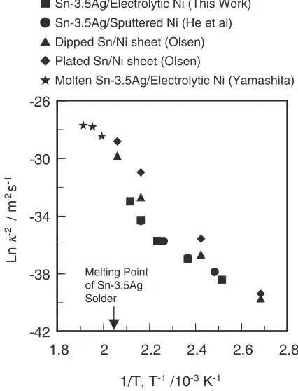
As shown in Fig. 15(b), the growth rate of the Sn–3.5Ag solder/Ni UBM at 463 and 473 K was slightly higher than expected from the Arrhenius plot between 398 and 448 K. This tendency was also seen in Sn–3Ag–0.5Cu solder/Ni UBM [Fig. 14(b)]. The activation energy in Sn–3.5Ag solder in the higher-temperature region is estimated to be 178 kJ/ mol, and in the lower-temperature region to be 80 kJ/mol, shown as the dotted line in Fig. 15(b). Similar results of accelerated growth at higher aging temperature can be found in previous reports, but without any discussion3,10,16)except for Yoon et al.5) Figure 17 shows growth rates in several systems of high Sn and pure Ni, which were re-plotted from previous works.10,16,17)Because these data show fairly good
agreement, this result is essential. Yoonet al.reported similar results in Sn–0.7Cu solder/Cu/Ni/Au UBM at temperatures between 343 and 443 K. In addition, the growth rate of the total IMC layer after aging for4:32106s at 443 K becomes
very high due to the formation of (Ni,Cu)3Sn4 added to the
original (Ni,Cu)6Sn5 layer.5) However, as the EPMA line
profile of the IMCs as shown in Fig. 13, the Sn–Ag solder joint has mono Ni3Sn4 IMC in this work. Therefore, this
result differs essentially from the results of Yoonet al.5)From the results of Sn–3Ag–0.5Cu solder, the growth rate of the low-temperature region has been somewhat accelerated by adding Cu. The activation energy change implies that the contribution of grain boundary diffusion diminishes and the
volume diffusion predominates as the layer grows thicker and grain coarsening progresses.
3.3 Void formation at the IMC/solder interface
When the aging temperature was at 473 K, large voids were observed in the Sn–3Ag–0.5Cu solder after0:72106s and in the Sn–3.5Ag solder after1:8106s. They were also observed in the Sn–3Ag–0.5Cu solder at 463 K after0:72
106s and in the Sn–3.5Ag solder after 1:8106s. During the solid state interactions, Kirkendall voids are often formed at the interface of the IMC and solder. However, since an Ni
0 2 4 6 8
0 1 2 3
(a)
(b)
Aging Time, t0.5/10-3s0.5
Thickness of IMC Layer, w /
µ
m
Ln
κ
2
/ m
2s
-1
1/T, T-1/10-3K-1
398K
423K
448K
-39 -37 -35 -33 -31
[image:7.595.118.479.75.266.2]20 22 24 26
Fig. 16 (a) Average thickness of the IMC layer of Sn–37Pb solder/electrolytic Ni joints with aging time and temperature and
(b) Arrhenius plot for the growth of the IMC layer.
Ln
κ
2
/ m
2s
-1
1/T, T-1/10-3K-1 -42
-38 -34 -30 -26
1.8 2 2.2 2.4 2.6 2.8
Sn-3.5Ag/Electrolytic Ni (This Work)
Sn-3.5Ag/Sputtered Ni (He et al) Dipped Sn/Ni sheet (Olsen)
Plated Sn/Ni sheet (Olsen)
Molten Sn-3.5Ag/Electrolytic Ni (Yamashita)
Melting Point of Sn-3.5Ag Solder
Fig. 17 Arrhenius plot for the growth of the IMC layer including the
[image:7.595.319.532.327.606.2]layer still remains in the sample, the void formation is not attributed to Ni consumption. Under the conditions in which the voids formed, Ni atom supply was limited due to diffusion through thick IMC. Therefore, Sn diffusion may predominate over Ni at the interface of IMC and solder. These voids were the result of unbalanced elemental diffusion. However, the voids were only observed at the center of contour line between the IMC and solder, not in the peripheral area. This shows the influence of other factors.
The outer parts of IMC swelled in Figs. 9, 11. This implies that the formation of IMC caused the volume expansion of the original Ni layer and reduction of the solder body. This led to the generation of shear stress along the outer radical direction at the interface between the IMC and solder. Shear stress may induce the accumulation of vacancies and deformation in the bumps to relieve the stress, and as a result of the formation of voids.
In Figs. 9, 11, some coarse Ag3Sn grains were formed in
the solder bodies. Ag3Sn and the IMC layer have strong
hardness and poor ductility.12) Since the surroundings of
Ag3Sn are especially heterogeneous in their mechanical
properties, it is presumed that voids are easily initiated at the area and propagated. The reason for there being no voids with the Sn–37Pb solder may be stress release by the ductile Pb phase accumulated at the interface.
4. Conclusions
In this work, we fabricated Sn–3Ag–0.5Cu solder, Sn– 3.5Ag solder and Sn–37Pb solder bumps with 110-mm
diameter solder balls on electrolytic Ni UBM, and inves-tigated the growth kinetics of intermetallic compound (IMC) layers and the morphology of bumps during long-term aging. (1) The IMC layer exhibited parabolic growth, and the activation energy values for the Sn–3Ag–0.5Cu, Sn– 3.5Ag and Sn–37Pb solder/Ni UBM were obtained with 95, 106 and 101 kJ/mol, respectively.
(2) The growth rate accelerated at 463 K or above in the Sn–3.5Ag solder. The activation energy for the
higher-temperature region is estimated to be 178 kJ/mol and for the lower-temperature region to be 80 kJ/mol. This tendency was also seen in the Sn–3Ag–0.5Cu solder. (3) (Ni,Cu)3Sn4 or Ni3Sn4IMC was formed mainly at the
solder/Ni interface after long-term aging.
(4) Large voids were formed at the interface between the solder and IMC at 463 K or above. The voids are the result of stress by volume expansion due to IMC growth. Coarse Ag3Sn grains were observed adjacent to
the voids and contributed to void initiation.
REFERENCES
1) D. Napp: SAMPE Journal32(1996) 59–65.
2) K. H. Lau:Flip Chip Technologies, (McGraw-Hill, New York, 1995)
25–28.
3) J. W. Yoon, S. W. Kim and S. B. Jung: Mater. Trans.45(2004) 727–
733.
4) A. Sharif, M. N. Islam and Y. C. Chan: Mater. Sci. Eng. B113(2004)
184–189.
5) J. W. Yoon, S. W. Kim and S. B. Jung: J. Alloys Compd.391(2005)
82–89.
6) K. Zeng and K. N. Tu: Mater. Sci. Eng., Elsevier Science, R38(2002)
55–105.
7) C. Y. Liu, K. N. Tu, D. R. Frear and P. Elenius: J. Appl. Phys.87(2000)
750–754.
8) Y. Kariya, K. Nakamura, Y. Tanaka and M. Otsuka: 6th Symp on
MATE, JWS(2000) 217–222.
9) M. He, W. H. Lau, G. Qi and Z. Chen: Thin Solid Films462–463
(2004) 376–383.
10) M. He, A. Kumar, P. T. Yeo, G. J. Qi and Z. Chen: Thin Solid Films
462–463(2004) 387–394.
11) Y. D. Jeon, A. Ostmann, H. Reichl and K. W. Paik:Proc. 53th ECTC,
IEEE(2003) 1203–1208.
12) D. Li, C. Liu and P. P. Conway: Mater. Sci. Eng. A391(2005) 95–103.
13) E. Hashino, K. Shimokawa, Y. Yamamoto and K. Tatsumi:Proc. 51th
ECTC, IEEE(2001) 957–964.
14) S. Terashima, Y. Kariya and M. Tanaka: Mater. Trans.45(2004) 637–
680.
15) W. T. Chen, C. E. Ho and C. R. Kao: J. Mater. Res.17(2002) 263–266.
16) D. Olsen, R. Wright and H. Berg:13th Ann. Proc. Reliability. Phys.
SymP., (1975) 80–86.
17) S. Yamashita, M. Harada, K. Yamamoto and R. Kimoto:37th MATE,