TEM Sample Preparation for Microcompressed Nanocrystalline Ni
Satoko Kuwano
1;2, Takeshi Fujita
2, Deng Pan
2;3, Ke Wang
3;*1and Mingwei Chen
2;3;*21HI-TECH Research Center, Tohoku Gakuin University, Tagajo 985-8537, Japan
2International Frontier Center for Advanced Materials, Institute for Materials Research, Tohoku University,
Sendai 980-8577, Japan
3World Premier International Research Center, Tohoku University, Sendai 980-8577, Japan
Ultra-large compressive plasticity at room temperature has recently been observed in electrodeposited nanocrystalline nickel (nc-Ni) under micro-scale compression (Pan, Kuwano, Fujita, Chen, Nano Letters 7, 2108 (2007)). The evolution of microstructure of nc-Ni during ultra-large deformation is outlined at a variety of strain levels, with TEM observations in combination with a TEM sample preparation technique using focused ion beam (FIB).
This paper demonstrates focused ion beam (FIB) technique to prepare transmission electron microscopy (TEM) samples from microcompressed specimens. There has been a demand to prepare TEM samples from a point of interest to study microstructures on atomic scales. Conventional techniques used to make TEM samples, such as chemical polishing or ion-sputtering milling, cannot provide reliable opportunity to make TEM samples from a point of interest. With this technique, the deformation mechanism on atomic scales can be fairly connected with the result of microcompression test, which is available for size-limited materials. [doi:10.2320/matertrans.MRA2008153]
(Received May 7, 2008; Accepted June 13, 2008; Published July 30, 2008)
Keywords: Focused Ion Beam, damaged layer, nanocrystalline nitride, deform, Transmission Electron Microscopy, nanoindentation
1. Introduction
The FIB instrument has become a significant method for the sample preparation for transmission electron microscopy (TEM).1)An advantage of the FIB method is that it is feasible to create a thin section at a point of interest using a rapid and precise procedure. The usage of the FIB instrument is not limited for only TEM sample preparation. The capability of the precise surface nanofabrication and the synchronous scanning ion image sensitive to crystallographic orienta-tions2)and atomic numbers3)led to development of a dual-beam FIB instrument.4)Accordingly, the enormous applica-tions of FIB are now widely spread from a nanotechnology perspective.
A compression test is a suitable method to understand the stress-strain behavior of various materials on mechanical property. In particular, the microcompression test is helpful to understand the deformation mechanism of a sample when the dimensions are limited such as films. In previous works, a nanoindentation apparatus can be utilized for a microcom-pression test for a microsized cylindrical sample fabricated by FIB.5)Recent studies show a significant sample-size affect on the stress-strain behavior indicating that the microcylinder size influences the underlying deformation mechanism.6) Therefore, a reliable and rapid procedure for the TEM observation after the microcompression test-using FIB is required. In terms of TEM sample preparation, the FIB technique comprises two major procedures; H-bar method and lift-out method. In the former, trenches are fabricated to create a path for the electron beam for TEM.7–9)In the lift-out method, a small sample was extracted from a point of interest of a bulk by a microprobe and the extracted piece was further fabricated to be a thin-wedged sample.10–13)In this paper, the lift-out method was applied rather than the H-bar method. A
nanocrystalline Ni produced by electrodeposition was chosen as a target in this study because its deformation mechanism under compression remains unclear due to the limited sample size. In order to evaluate the sensitive microstructure of the nanocrystalline Ni, a damage investigation of the FIB technique is essential. Therefore, we have discussed a damaged amorphous layer and contamination induced by FIB.
2. Experimental Process and Results
High purity nc-Ni specimens with a thickness of200mm were synthesized by aqueous electrodeposition using a sulfa solution that contains 460–520 mL/L Ni, 35–50 mL/L boric acid, and 15–20 mL/L NiCl2
.6H
2O. (502C, pH = 3.5– 4.5).14)The result of a chemical analysis performed by atom probe tomography shows that the Ni plate is highly pure and only trace impurity elements such as Fe and S are detected (with concentrations of tens of ppm) uniformly distributed in the grains. XRD measurements of the as-deposited nc-Ni coupon excluded that noticeable textures exist in the nano-grains. The grain size distributions of the as-deposited and deformed nc-Ni were characterized by transmission electron microscopy.A focused ion beam (FIB) apparatus (Hitachi High-Technologies Corporation FB-2100) was used to fabricate the Ni plate for obtaining a microsized cylinder and a TEM sample from the deformed microcylinder. An FIB column in the instrument supplies Ga ions accelerated at 40 kV and beam currents in the range 0.01 nA to 35 nA. Cylindrical micropillars for microcompression tests were fabricated by a Hitachi FB-2100 focused ion beam system. Subsequent fine-milling processes were applied with lower fine-milling currents (e.g. 0.02 nA) and acceleration voltage (e.g. 40 kV) thereafter to carefully eliminate the visible tapering of sidewalls of the sample. A schematic of the fabrication procedure of micropillars are shown in Figure 1. The FIB column has
*1Graduate Student, Tohoku University
*2Corresponding author, E-mail: [email protected]
a W deposition system in its chamber for depositing the W protective layer. In addition, FIB can be used to fix an extracted small fragment on a TEM grid by W deposition.
A nanoindentation apparatus (SHIMADZU DUH-W20S) equipped with a flat-end diamond indentation tip with a diameter of 10mm was employed to carry out the compression tests at room temperature. Prior to each micro-compression test, the indentation apparatus was finely tuned by measuring level condition around the cylindrical micro-pillar to avoid off-axis loading of the sample. The indented depth set the compression strain. Microcylinders were compressed at room temperature with different loading rates ranging from 0.132 mNs1 to 70 mNs1.
The TEM apparatus (JEOL JEM-3010) used at 300 kV provided microstructure observation with an atomic resolu-tion. It is equipped with energy dispersive X-ray spectrom-etry (EDS) to determine the components.
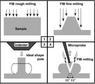
Figure 1 shows a schematic procedure to make a micro-cylinder and a TEM sample-using FIB for microcompression test. The fabrication procedure basically follows the previous reports.6,15,16)After obtaining a smooth surface morphology of the electrodeposited Ni plate by polishing with a diamond paper of 1mmroughness, a microcylinder was engraved on the sample by FIB. As a rough milling step for rapid process, a condition of a high beam current of 6:40:3nA and a voltage of 40 kV was applied to obtain a imperfect micro-cylinder with a diameter of 4mm(Fig. 1, step 1). Next, as a fine milling step, a side of the microcylinder was milled with a small ion current of0:070:01nA and a voltage of 40 kV in order to obtain a perfect cylindrical shape. Then, we could obtain an ideal cylindrical shape with a diameter of 3:7
0:1mm and a height of 7:80:1mm for the following microcompression test (Fig. 1, step 2). The aspect ratio of the height to the diameter was set to approximately 2:1.
The indentation apparatus need to be fine-tuned and aligned to compress the microcylinder uniaxially. Before the indentation, we carried out four times test-indentations around the cylinder in order to predict the accurate distance between the cylinder and the indentation tip. Then the long axis of the cylinder was set along the indentation direction. Next, the cylindrical samples were deformed with several different loads and deformation rates by changing the indentation speed and the indentation depth (Fig. 1, step 3). Figure 2(b) shows an example of a deformed microcylinder. The compressed microcylinder was a drum-like shape without a fracture. Figure 2(c) shows a true stress-strain curve of the microcompresion test. The applied stress was reached to 1.5 GPa at the strain of 0.4.
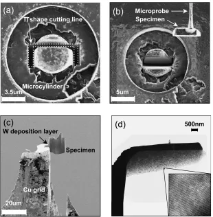
After the microcompresion test, the microcylinder was again placed back in the FIB chamber to clip the wedge from compressed pillar (Fig. 1, step 4). First, the deformed micro-pillar was milled from a tilted angle from the top to +11
using a FIB beam with accelerated voltage of 40 kV. A top view of the milled trace showed a resemblance to the Greek letter ‘‘’’ (Fig. 3(a)). Next, the sample was tilted to11
and a microprobe was attached on the top surface of the micropillar by W deposition. After removing the residual portion, the wedge-shaped TEM specimen was detached from the micropillar by using a microprobe (Fig. 3(b)). The wedge was subsequently lift out and attached on to a half-cut Cu grid by W deposition, followed by removal of the microprobe tip part from the TEM sample by Ga ion Fig. 1 Schematic diagrams of experimental procedures (a) FIB rough milling of micropillar in the bulk nanocrystalline nickel coupon;
[image:2.595.142.454.73.348.2]Fig. 2 SEM micrographs of the microcylinder (a) undeformed; (b) deformed to 70 mN/s and imposed strain of 0.4. (c) Representative stress-strain curves of the microcylinder on (b).
[image:3.595.131.467.72.366.2] [image:3.595.144.454.420.736.2]Ga atoms easily diffuse into the bulk materials. This investigation is important for minimizing Ga contamination during FIB milling on the mechanical response of the micropillar. According to Ref. 17, Ga ions can interact with other elements and phases to form amorphous layers, solid-saluted alloy and precipitate. And a Gaþ implantation and
damage occurring in surface of the micropillar creates a damage layer with a thickness of 10–100 nm.18,19) This damage layer may strengthen the specimen by restricting the emission of dislocation from the surface.20,21)To evaluate the influence of this layer in the mechanical behavior of nc-Ni, chemical analysis of the longitudinal section of deformed nc-Ni is carried out. Therefore, the effect of Ga must be concerned with Ga contamination and ion damage.
In order to minimize the damaged amorphous layers, moderate-milling conditions such as low voltage, low current,22,23)and low incidence angle24)were proposed. We reduced the acceleration voltage of Ga ions in the FIB from 40 kV to 10 kV for studying its effect. However, the thickness of the damaged amorphous layer did not change significantly. We could observe a high-resolution TEM image under the acceleration voltage of 40 kV accompanied with the inci-dence angle less than 8 and current density less than
0.2 nA/mm2. Under the experimental condition, the thickness of the amorphous layer was less than 5 nm in our experiment. We could get TEM and EDS observation results of nano crystalline Ni as show on Fig. 4 under these experimental condition.
In EDS experiment, we attempted to detect Ga atoms at the three points on the sample, (A) The right below of microp-robe, (B) the surface of cylindrical pole sample, and (C) the edge of the FIB-treated wedge shape. The EDS profile in Fig. 4(d) show the existence of W and Ga at position A, cause of fixing a micro probe with a sample by W deposition and Ga beam. The EDS profile at position B and C did not show notable Ga peaks. From these results, there is no significant Ga contamination in micro pole.
TEM image on Fig. 4(b) is an edge of sample on position C. It is possible to have amorphous layer on the surface and edge by Ga beam during milling process as Fig. 4(c). In our experiment, we could observe an amorphous layer along a thin edge. Under the experimental condition, the thickness of the amorphous layer was less than 5 mm in our experiment. From this observation, there is no significant influence on the mechanical behavior such as ductility of the nc metal, other than a presumably overestimated strength.
In order to clarify the effect of Ga ions on nanocrystalline Ni, we also prepared undeformed specimens using both FIB
and electropolishing technique. Regarding to the electro-polishing procedure, the samples were sliced and ground mechanically and finally electropolished in a solution of 10% H2SO4, 10% CH3OH and 80% C2H5OH. We also prepared an FIB-milled specimen from the undeformed microcylinder. Overall, the electropolished and the FIB-milled specimens were compared by using TEM, respectively (Figs. 5(a) and (b)). The grains were uniformly shaped, and the average size was in the range of 20 to 30 nm in the both cases. Therefore, we can rule out the grain growth due to local temperature increment and ion damage.
4. Conclusions
We established a standard procedure of the FIB technique to prepare TEM samples for the purpose of microcompres-sion test. The thickness of the damaged layer containing Ga was found to be considerably thin, which was confirmed by TEM. Upon this study, we can certainly access the size-limited nanostructured materials and reveal the deformation mechanism using a nanoindentation apparatus.
Acknowledgements
We acknowledge 21st Century COE program at Institute for Materials Research, Tohoku University.
[image:4.595.347.507.70.375.2]REFERENCES
1) L. A. Giannuzzi and F. A. Stevie: Micron30(1999) 197–204. 2) Y. Yahiro, K. Kaneko, T. Fujita, W.-J. Moon and Z. Horita: J. Electron.
Mater.53(2004) 571–576.
3) T. Ishitani, Y. Madokoro, W. Nakagawa and K. Ohya: J. Electron. Mater.51(2002) 207–213.
4) V. G. M. Sivel, J. Van den Brand, W. R. Wang, H. Mohdadi, F. D. Tichelaar, P. F. A. Alkemade and H. W. Zandbergen: Journal of Microscopy214(2004) 237–245.
5) M. D. Uchic and D. M. Dimiduk: Mater. Sci. Eng. A400–401(2005) 268–278.
6) M. D. Uchic, D. M. Dimiduk, J. N. Florando and W. D. Nix: Science
305(2004) 986–989.
7) C. R. Perrey, C. E. Carter, J. R. Michael, P. G. Kotula, E. A. Stach and V. R. Radmilovic: J. Microscopy214(2004) 222–236.
8) M. Saito, T. Aoyama, T. Hashimoto and S. Isakozawa: Jpn. J. Appl. Phys.37(1998) 355–359.
9) M. Sugiyama and G. Sigesato: J. Electron. Mater.53(2004) 527–536. 10) A. E. M. De. Veirman: Mater. Sci. Eng. B102(2003) 63–69. 11) N. Bicais-Lepinay, F. Andre, R. Pantel, S. Jullian, A. Margain and L. F.
Tz. Kwakman: Microelectronics Reliability42(2002) 1747–1752. 12) R. D. Field and P. A. Papin: Ultramicroscopy102(2004) 23–263.
13) Z. Huang: Journal of Microscopy215(2004) 219–223.
14) F. Ebrahimi, G. R. Bourne, M. S. Kelly and T. E. Matthews: NanoStructured Materials11(1999) 343–350.
15) J. Greer, W. C. Oliver and W. D. Nix: Acta Mater.53(2005) 1821– 1830.
16) J. R. Greer and W. D. Nix: Phys. Rev. B73(2006) 245410(6). 17) J. Marien, J. Plitzko, R. Spolenak, R. M. Keller and J. Mayer:
Journal of Microscopy194(1999) 71–78. 18) R. M. Langford: Microsc. Res. Tech.69(2006) 538.
19) M. D. Uchic and D. M. Dimiduk: Mat. Sci. Eng. A400–401(2005) 268.
20) H. Bei, S. Shim, M. K. Miller, G. M. Pharr and E. P. George: Appl. Phys. Lett.91(2007) 111915.
21) T. Zhu, J. Li, A. Samanta, H. G. Kim and Suresh S: Proceedings of the National Academy of Science of the United States of America
104(2007) p. 3031.
22) N. I. Kato, Y. Kohno and H. Saka: J. Vac. Sci. Technol. A17(1999) 1201–1204.
23) T. Kamino, T. Yaguchi, Y. Kuroda, T. Ohnishi, T. Ishitani, Y. Miyahara and Z. Horita: Journal of Electron Microscopy53(2004) 459–463.
24) J. P. McCaffrey, M. W. Phaneuf and L. D. Madsen: Ultramicroscopy87
(2001) 97–104.
[image:5.595.145.452.73.220.2]