Microstructure Analysis of High Coercivity PLD-Made Nd-Fe-B Thick-Film
Improved by Tb-Coating-Diffusion Treatment
Masahiro Ishimaru
1;*, Masaru Itakura
1, Minoru Nishida
1,
Masaki Nakano
2and Hirotoshi Fukunaga
21Department of Applied Science for Electronics and Materials, Kyushu University, Kasuga 816-8580, Japan 2Department of Electrical and Electronic Engineering, Nagasaki University, Nagasaki 852-8521, Japan
Microstructure of high coercive pulsed laser deposition (PLD) made Nd-Fe-B thick-film magnet improved by ‘‘Tb-coating-diffusion’’ treatment has been investigated with an analytical transmission electron microscope (ATEM). It was found that the PLD-made film consists mainly of fine Nd2Fe14B grains about 200 nm in diameter and a large amount of Nd intergranular phases. Energy dispersive X-ray spectroscopy
(EDS) analysis showed that each Nd2Fe14B grain is covered with a thin (Nd,Tb)2Fe14B layer about 20–30 nm in thickness and thin Nd-Tb
grain-boundary-layer about 5–10 nm in width. The present results indicate that such a two-layered-wrapping structure enhances significantly the coercivity of the PLD-made thick-film magnet. [doi:10.2320/matertrans.M2010189]
(Received May 31, 2010; Accepted July 21, 2010; Published September 8, 2010)
Keywords: neodymium-iron-boron permanent magnet, film magnet, coercivity, pulsed laser deposition (PLD), Tb-coating, Analytical transmission electron microscopy (ATEM), energy dispersive X-ray spectroscopy (EDS)
1. Introduction
Nd-Fe-B film magnet attracts much attention in the field of electronic devices such as millimeter size motors and micro-actuators. Nakano et al.1–3)have reported that isotropic Nd-Fe-B thick-film magnets can be produced by pulsed laser deposition (PLD) method under the high deposition rate up to 25 nm/s. They have also found that anistropic Nd-Fe-B thick-film magnets are successfully prepared by the PLD method with a substrate heating system.3,4)
In these days, demands for the higher coercive thick-film magnets are increasing rapidly in order to withstand the applications at elevated temperatures. It is well known that partial substitution of Dy or Tb for Nd in the Nd2Fe14B grains
increases the magneto crystalline anisotropy and then enhances the coercivity of the magnet. In the case of sintered magnets, it begins to be pointed out that a continuous thin grain boundary phase exists around each Nd2Fe14B grain and
the capsule structure would enhance the coercivity.5,6) Furthermore, it has already been reported that the coercivity seems to increase greatly by penetrating Tb into the thin grain boundary phase.7,8)
Recently, some of the present authors9) found that the coercivity of the isotropic PLD-made Nd-Fe-B thick-films can be enhanced by applying ‘‘Tb-coating-diffusion treat-ment’’. In this study, the microstructure of the Tb-treated PLD-made Nd-Fe-B thick-film was investigated in details with analytical transmission electron microscope (ATEM), in order to understand the origin of the coercivity enhancement.
2. Experiments
20-mm-thick Nd-Fe-B films were deposited on 40-mm -thick Ta substrates at room temperature by the PLD method using a Nd2:4Fe14B target. The typical deposition rate was
about 6 nm/s. X-ray diffraction (XRD) analysis showed that the crystal structure of the as-deposited Nd-Fe-B films was amorphous. Subsequently, 2-mm-thick Tb was deposited on the Nd-Fe-B film, and then the obtained two-layered film was crystallized by heating up to about 923 K with a heating rate of about 6.7 K/s in an infrared furnace.
Hysteresis loops of the thick-film specimens were meas-ured with a vibrating sample magnetometer (VSM). The microstructures were observed with TEMs (FEI TECNAI-20F and JEM 2000EX). Elemental analysis was carried out with the TEM equipped with a beam-scanning (STEM) and an energy dispersive X-ray spectroscopy (EDS) system. Cross-sectional TEM specimens were fabricated using a focused ion beam (FIB: HITACHI FB-2000K) mill with a micro-sampling unit.
3. Results and Discussion
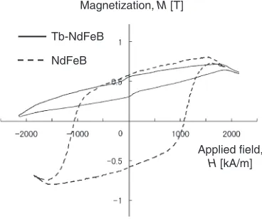
Figure 1 shows M-H curves of the PLD-made Nd-Fe-B thick-films without or with the Tb-coating-diffusion treat-ment. The Tb-treated thick-film shows a notable increase (twice or more) of the coercivity without decrease in remanence.
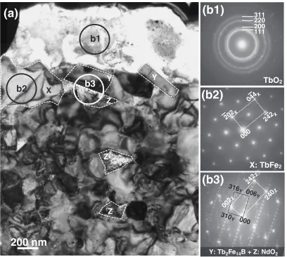
Figure 2 shows a low magnification TEM bright field (BF) image of the PLD-made Nd-Fe-B thick-film with the Tb-diffusion coating treatment. One can see that the PLD-made thick-film consists fundamentally of fine grains with sub-micrometer in diameter, except for a large droplet at the top surface. Figure 3(a) shows an enlarged TEM-BF image of the region A (the top part) in Fig. 2. A bright layer about 400 nm in thickness is covered continuously on the top surface. Also, isotropic crystal grains (grains X) about 400 nm in diameter and anisotropic rectangular grains (grains Y) about 200– 500 nm in length are formed under the white layer. Selected area electron diffraction (SAED) patterns taken from the areas b1–b3 in Fig. 3(a) are shown in Figs. 3(b1)–(b3), respectively. The SAED from area-b1 shows a ring pattern for a face-centered cubic (fcc) phase, and the corresponding
*Graduate Student, Kyushu University. Present address: Kobelco Research
Institute, Inc., Kobe 651-2271, Japan
EDS analysis indicates that the area-b1 is composed of terbium and oxygen elements. Therefore, the white layer in Fig. 3(a) consists of randomly oriented TbO2 nanocrystals,
which are formed by an oxidation of the remaining deposited Tb-layer. The area-b2 can be identified as a TbFe2grain with
a cubic C15 Laves phase structure (MgCu2-type),10)so TbFe2
crystal grains are formed near the top surface. The TbFe2
Laves phase is known to be the material with the highest magnetostriction at room temperature.11) It is thought that
the formation of TbFe2 phase causes a little drop of
magnetization. However, the influence of this phase is very small according to the magnetization curve with the solid line in Fig. 1. The SAED from the area-b3 can be explained by superimposed patterns of reflections from a tetragonal phase with a Nd2Fe14B structure (P42/mnm)12)and a NdO2 phase
with a fcc structure.13) Although we do not reproduce the
EDS spectrum and elemental maps of this area, the following results were obtained. The rectangular grains (grains Y) in Fig. 3(a) were a hard magnetic Tb2Fe14B phase. In the top
part of the film, therefore, a lot of NdO2 grains (grains Z)
were formed around the angular Tb2Fe14B grains (grains Y)
and the isotropic TbFe2grains (grains X).
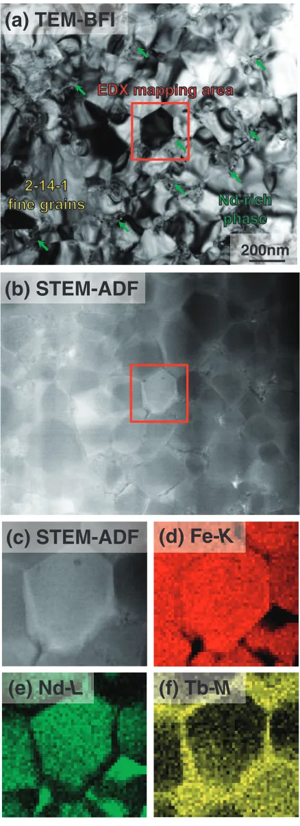
Figure 4(a) shows an enlarged TEM-BF image of the region B in Fig. 2. The middle part of the thick-film consists mainly of fine Nd2Fe14B grains about 200–300 nm in
diameter, which is comparable to the single magnetic domain size,14) and the size of Nd
2Fe14B grain is almost the same
as that in the PLD film without the Tb-coating treatment. However, the number of angular-shaped Nd2Fe14B grain
with facetted boundaries increases by applying the Tb treatment. Moreover, a large amount of intergranular phase with a strain contrast is formed at the triple junction of the Nd2Fe14B grains as indicated by green arrows in Fig. 4(a).
The intergranular phase was composed of almost pure Nd. A STEM annular dark field (ADF) image obtained from the same area is shown in Fig. 4(b). One can notice that grain-boundary-layer forms in the surroundings of Nd2Fe14B
grains. The grain-boundary-layer has a bright contrast compared with the Nd2Fe14B grains, which indicates that
the grain-boundary-layer is composed of relatively heavy elements. Figures 4(c)–(f) show an enlarged STEM-ADF image and EDS elemental maps obtained from the area marked with a red square in Fig. 4(a), respectively. One can see that Tb is enriched at the surface layer about 20–30 nm in thickness of Nd2Fe14B grains about 200 nm in diameter as
seen in Fig. 4(f). In other words, the substitution of Tb for a part of Nd occurs and then (Nd,Tb)2Fe14B layer is formed
near the surface of Nd2Fe14B grain. Moreover, it can be seen
in Figs. 4(d), (e) and (f) that a very thin Nd-Tb layer (about 5–10 nm in thickness) without Fe exists at the grain boundary. In order to complete more quantitative estimation, we have to obtain EDS data systematically. From the present results, however, it is evident that each Nd2Fe14B grain is wrapped
by two layers consisting of thin (Nd,Tb)2Fe14B layer and
thin Nd-Tb grain boundary layer. These results indicate that the surplus Nd by forming the (Nd,Tb)2Fe14B layer produces
a large amount of the Nd intergranular phase.
A similar analysis was carried out for the lower part of the thick-film at the region C in Fig. 1. The results are shown in Figs. 5(a)–(e). One can obviously see that the two-layered-wrapping structure is also formed in the bottom part of the thick-film. The thickness of the Tb-enriched layer seems to be thin a little when becoming in the bottom part beacause of diffusivity of Tb.
The wrapping structures of Nd2Fe14B grains have been
reported in several sintered magnets.7,8,15,16) Park et al.15) reported that by applying Dy-metal coating and consecutive optimum heat treatment, Nd2Fe14B grains having
Dy-enriched surface are formed and then the coercivity improves
Droplet
Region A
Region B
Region C
FIB damage
1
µ
m
Fig. 2 Cross-sectional TEM bright field (BF) image of the PLD-made Nd-Fe-B thick film with the Tb-diffusion coating treatment after crystalliza-tion.
Magnetization, M [T]
Applied field, H [kA/m] Tb-NdFeB
NdFeB
[image:2.595.76.260.74.228.2] [image:2.595.48.290.281.617.2]by the twice. Suzuki and Machida16)found that the degraded
coercivity of small-sized Nd-Fe-B sintered magnets can be successfully recovered by the surface treatment with Dy- and Tb-metal vapor sorption. Some of the present authors7,8)have
been reported that the Tb-treatment allows the formation of the thin and continuous grain-boundary-layer around Nd2Fe14B grains. In these techniques, however, the wrapping
structure can be formed only to the range of about 50mm
from the surface of the magnet. Moreover, a large amount of Dy is consequentially consumed because Dy diffuses widely into the Nd2Fe14B grains. In the case of sintered magnets,
it is important to form the grain boundary structure whose restraints the reversal of magnetic domains (or passivation of the grain surface), because the coercivity mechanism is thought to be a nucleation type of reversed magnetic domain. In the PLD-made thick-film magnets, on the other hand, it is necessary to make microstructures with high pinning force of the magnetic wall. From this point of view, the two-layered-wrapping structure observed in the present study is extremely effective for generating the coercivity. The coercive force is expected to increase by applying the Tb-coating-diffusion treatment because the pinning force increases with the thickness of the grain-boundary-layer and the magnetocrys-talline anisotropy of the grain boundary phase.17)
In the Tb-coating-diffusion treatment, a uniform wrapping structure can be formed in the wide area of several tenmm, though the amount of Tb used is relative small. However, it is a problem that the surplus Nd by forming the Tb-enriched layer produces a large amount of the Nd intergranular phase. Furthermore, the deposited Tb remains in the top surface of the thick-film as the TbO2microcrystalline layer. Therefore,
it is effective to make a multi-layered structure of the Nd-Fe-B and the Tb thin-film layers to improve further uniformity of wrapping structure and decrease the amount of Tb consumption.
4. Conclusion
We have investigated the detailed microstructure of the Tb-treated PLD-made thick-film by TEM and STEM-EDS analyses. By applying the Tb-coating-diffusion treatment, each Nd2Fe14B grain is wrapped with (Nd,Tb)2Fe14B layer
and thin Nd-Tb grain boundary layer. This two-layered-wrapping structure is formed in the almost whole area of the PLD film more than 10mmin thickness except for the top surface. It is concluded that the dramatic increment of coercivity without decreasing the remanence is caused by the formation of the two-layered-wrapping structure.
200 nm
(a)
(b1)
(b2)
(b3)
b1
b2
b3
111 311 200 220
TbO2
000 202X
044X
242X
X: TbFe2
Y: Tb2Fe14B + Z: NdO2
000
240
Z
242
Z
310
Y
316
Y 006 Y
002
Z
Y
Z
Z
Y
X
Z
[image:3.595.95.503.70.436.2](c) STEM-ADF
(d) Fe-
K
(e) Nd-
L
(f) Tb-
M
(b) STEM-ADF
(a) TEM-BFI
200nm
Fig. 5 (a) TEM-BF image of lower part of the PLD-made Nd-Fe-B thick film with the Tb-diffusion coating treatment corresponding to the region C in Fig. 2. (b) STEM-ADF image and (c)–(e) EDS elemental mapping images obtained from the area marked with a red square in (a). (c) Fe-K, (d) Nd-L, and (e) Tb-Mmaps.
(a) TEM-BFI
(b) STEM-ADF
(c) STEM-ADF (d) Fe-
K
(e) Nd-
L
(f) Tb-
M
200nm
[image:4.595.58.278.68.723.2] [image:4.595.317.536.71.674.2]Acknowledgement
The authors would like to thank Mr. S. Ohta and Ms. N. Watanabe of Kyushu University for technical support. This study was partly supported by Grants-in-Aid for Scientific Reserch (B) (#21360342) from the Japan Society for the Promotion of Science. The first author is grateful for financial assistance provided by the Global-Centre of Excellence in Novel Carbon Resource Sciences, Kyushu University.
REFERENCES
1) M. Nakano, R. Katoh, H. Fukunaga, S. Tutumi and F. Yamashita: IEEE Trans. Magn.39(2003) 2863–2865.
2) M. Nakano, R. Kato, S. Hoefinger, J. Fidler, F. Yamashita and H. Fukunaga: J. Alloy. Compd.408–412(2006) 1422–1425.
3) M. Nakano, S. Sato, F. Yamashita, T. Honda, J. Yamasaki, K. Ishiyama, M. Itakura, J. Fiedler, T. Yanai and H. Fukunaga: IEEE Trans. Magn.43(2007) 2672–2676.
4) M. Nakano, S. Sato, H. Fukunaga and F. Yamashita: J. Magn. Magn. Mater.303(2006) e375–e378.
5) F. Vial, F. Joly, E. Nevalainen, M. Sagawa, K. Hiraga and K. T. Park: J. Magn. Magn. Mater.16(2002) 1329–1334.
6) W. F. Li, T. Ohkubo and H. Hono: Acta Mater.57(2009) 1337–1346. 7) N. Watanabe, M. Itakura, N. Kuwano, D. Li, S. Suzuki and K.-I.
Machida: Mater. Trans.48(2007) 915–918.
8) N. Watanabe, H. Umemoto, M. Ishimaru, M. Itakura, M. Nishida and K. Machida: J. Microsco.236(2009) 104–108.
9) M. Nakano and H. Fukunaga: Private Communications. 10) C. M. Gilmore and F. E. Wang: Acta Cryst.23(1967) 177–179. 11) A. E. Clark and H. S. Belson: Phys. Rev. B5(1972) 3642–3644. 12) J. F. Herbst, J. J. Croat, F. E. Pinkerton and W. B. Yelon: Phys. Rev. B
29(1984) 4176.
13) K. Makita and O. Yamashita: Appl. Phys. Lett.74(1999) 2056–2058. 14) J. D. Livingston: J. Appl. Phys.57(1985) 4137–4139.
15) K. T. Park, K. Hiraga and M. Sagawa: Proc. 16th Int. Workshop on Rare-Earth Magnets and Their Applications, ed. by H. Kaneko, M. Homma and M. Okada, Sendai, Japan, Vol. 1 (The Japan Institute of Metals, 2000) pp. 257–264.