Modular plug-in high-performance assembly of a power converter
A.K. Solomon, A. Castellazzi
The University of Nottingham, PEMC Group
Nottingham NG7 2RD, UK
Tel.: +44 / (0) – 1159515568
[email protected],
[email protected]
N. Delmonte, P. Cova
Department of Information Engineering
University of Parma, Italy
[email protected], [email protected]
Keywords: <<High power density>>, <<Packaging>>, <<System integration>>, <<Inverter>>, <<Thermal design>>
Abstract
This paper presents the work on an alternative integration scheme for a half-bridge switch using 70 μm thin Si IGBTs and diodes addressing higher strength, higher toughness and higher thermal conductivity. The switch is totally bond wireless, since bonded wires increase self-heating and introduce further thermomechanical degradation mechanisms. Moreover, this solution is equipped with double side liquid cooling, and plug-in edge connectors both on the driver and load sides, allowing high power density, good accessibility and modularity. Preliminary experimental results show good switching behavior.
1.
Introduction
The power modules are widely spread, for very different applications, such as industrial electric motor driving and welding, automotive and conversion of renewable energy. At the same time, the required features of the power converters are increasingly stringent in terms of occupied volume, power quality, efficiency, reliability, maintainability, modularity, and cost. Several works can be found in the literature proposing different solutions at module level, rather than at system level (power modules together with heatsinks, drivers, connectors, and anything else needed). State-of-the-art techniques applied to power modules may require the study and the development of new components to realize the conversion system. The design of customized components connected to a new power module is sometimes mandatory to do not wipe away the performances obtained by the new module. Typical solutions can be found for specific issues like integration and cooling of power module [1]-[5], or implementing highly integrated systems to reduce the stray inductances [6]. These include at times gate-drivers, power stage, and DC-link components in the same package [7].
use of a very efficient cooling system (based on air forced or liquid cooling heatsinks). In this case, the possibility of a double-sided cooling has been exploited, because of the stacked layout of the HBS. Figure 1 shows the schematic of the overall system. Parts in the dotted lines are the ones that can be considered as new solutions: the gate-driver connector, the HBS module, and the power connector. Some ceramic capacitors and resistors have been embedded in the connectors, with a capacitance suitable to filter switching ringing.
Fig. 1: Schematic of the single-phase inverter made with the proposed HBS module.
2.
Design and simulations
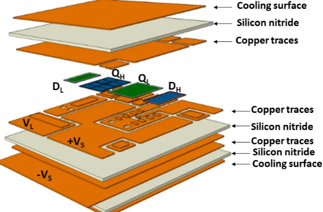
The design has been carried out with the aim to obtain a conversion system with innovative features and state-of-the-art performances. High integration, high reliability, extreme reduction of the parasitic to attain high efficiency conversion system along with power quality, modularity, and ease of assembly that make the converter more flexible and easy to repair, are the key features that needs to achieve with the development of the technology presented here. Figure 2 shows the exploded version of the 3D model of the HBS module. Waveforms of the collector-emitter voltage measured during early electrical tests have shown extremely clean switching transitions, confirming a very low parasitic inductance of the power loop [8].
[image:2.595.135.463.511.726.2]The use of ad-hoc components, materials and techniques, as well as a good design using the latest CAD software for electrical simulation (SPICE) and the physical simulation of 3D thermal, thermo-fluid-dynamic, electro-magnetic, and thermo-mechanical problems (ABAQUS, COMSOL, ANSYS) were considered at the early development stages. Here, particular attention is paid to physical simulations of the HBS and its edge connectors, to determine thermal and electro-magnetic behaviour.
For example, in order to obtain an efficient heat extraction by the HBS, the design of a liquid-cooled heatsink was carried out by means of a CFD (Computational Fluid-Dynamic) analysis using COMSOL Multiphysics 5.2.
The heatsink has been modelled as shown in Figure 3, coupling the non-isothermal fluid flow and the heat transfer in solid and liquid physics. As boundary conditions of the fluid domain where the Navier-Stokes equation has to be solved, were set at a flow rate of 4 l/min at the inlet, a reference pressure of 0 Pa at the outlet, and the no slip condition at the remaining boundaries. An inward heat transfer rate of 150 W on both water boundaries in contact with the cooling surfaces of the HBS was set. A natural air convection condition at all the external surfaces of the cooler made of polytetrafluoroethylene (PTFE), a fixed temperature of the water at the inlet Tinlet = 17 °C, and a normal heat flux at the outlet were also
applied.
[image:3.595.75.524.299.469.2][image:3.595.167.429.590.712.2]
Fig. 3: Boundaries conditions of the 3D COMSOL model taken as an example: fluid flow model (left); heat transfer model (right). is the normal unit vector and is the heat flux in a given point of the outlet boundary surface.
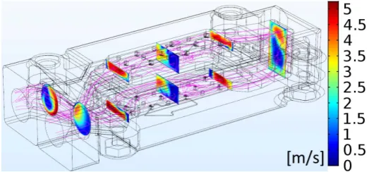
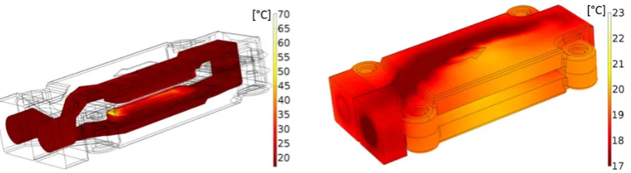
Figure 4 and Figure 5 show the results of CFD simulation fully coupled with HT (Heat Transfer) problem. It can be noticed, as expected, that the relevant vorticity is in the portion where the liquid is in contact with the HBS cooling surface: this improves the heat transfer coefficient. The total dissipated power (Pd) is 300 W, with a flow rate of 4 l/min and an inlet temperature of 17 °C.
Fig. 5: Water thermal map (left) and cooler’s external boundaries thermal map (right), with an inlet flow rate of 4 l/min, Tinlet = 17 °C, and Pd = 300 W.
As can be seen, the maximum temperature of the water is well below the boiling point at sea level (100 °C).
Usually, the coolant is a water-glycol mixture to achieve both freezing-point depression and boiling-point elevation. Pre-inhibited glycol solutions can also be used to prevent corrosion, and oxides or moulds deposition.
[image:4.595.188.407.409.562.2]Considering the next experimental setup, a series of thermal simulations, varying the flow rate (2.3÷12 l/min) and the temperature at the inlet (10÷25 °C), was carried out with an inhibited 40 vol% propylene glycol aqueous solution as coolant, whose physical properties have been taken by [9]. In order to estimate the temperatures inside the HBS module, it was added to the 3D COMSOL model (Figure 6). In this case, the heat source has been set inside the silicon subdomains of diodes and IGBTs. The maximum power dissipated by each IGBT (100 W) and each diode (50 W) has been estimated by SPICE simulations.
Fig. 6: 3D geometry of the HBS & heatsink assembly.
Figure 7 shows the thermal result obtained in the worst case with flow rate = 2.3 l/min, Tinlet = 25 °C,
and ambient temperature Tamb = 24 °C. The maximum temperature (∼ 92 °C) is in the diode close to the
cooler’s plug side. The maximum temperature reached by the IGBTs is around 77 °C. Considering the typical uncertainty of ± 10% on the simulation results, the highest temperature is near 100 °C, which is the maximum allowable temperature for reliability in the most commonly applications.
Fig. 7: Simulation results of the HBS+heatsink with flow rate = 2.3 l/min, Tinlet = 25 °C, Tamb = 24 °C, PIGBT = 100 W, Pdiode = 50 W: (a) external thermal map; (b) thermal map of the coolant at the walls; (c) thermal map of inner HBS layers viewing diodes and IGBTs dice.
The result of Figure 7 can be useful to estimate the thermal resistance of the assembly.
The thermal resistance of cold plates is given considering the difference between the maximum desired cold plate surface temperature and the temperature of the liquid coolant at the inlet. In this case we can refer to the maximum temperature in the module obtained by simulations to estimate the following thermal resistance:
= − =92 − 25
180 ≅ 0.37 ° /
3.
The HBS based system setup
The idea here was to design not only a new highly integrated sandwich half-bridge module, but also new connectors to keep the lengths of the connections as short as possible in order to have small stray inductances, both for gate and power loops as shown in Figure 8. With a stacked structure, it has been clearly shown that the electrical paths’ lengths between diodes and active devices of the HBS can be optimized, but the connections between the module and the supply, or the load and the drivers can be problematic with standard connectors.
[image:5.595.103.494.522.709.2]Starting from this, new quick-mount connectors with integrated capacitors and resistors have been designed, again to reduce the volume of the system as much as possible, together with fast mounting. Such connectors can be useful to the designers of a power converter, as the integrated capacitors can be suitable to decouple the DC source by the high frequency oscillations generated during switching, thus reducing the hassle in the design of the whole conversion system. With the same philosophy, the gate current limiter resistors are also embedded into the gate-driver connector.
[image:6.595.73.520.349.483.2]3.1.
The HBS module
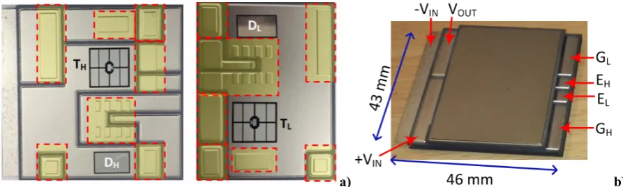
Figure 9 is the assembled HBS power module where the corresponding layers are depicted in Figure 2. The external silicon nitride layers are covered with two copper layers on which a cooling system can be mounted on both sides. Silicon nitride has been chosen for its mechanical properties, that can ensure high reliability as compared to other substrates (e.g. Aluminum Oxide, Aluminum Nitride). The switch assembly has been constructed using the latest generation Infineon Technologies 70 μm thin vertical IGBTs and diodes rated at 600 V, 200 A having maximum operating junction temperature of 175 °C. They are solderable and compatible with nonstandard non-wire-bond interconnection processes. To reduce the thermal resistance across solder joints it would be instinctive to minimize its thickness. However, a compromise is necessary to allow for mechanical integrity in the joints. So, the solder, whose layers are not depicted in Figure 2 for simplicity, is 100 μm thick Sn3.5Ag. It has been used to connect IGBTs and diodes with copper traces and to connect different layers of copper traces. The silicon nitride layers are 635 μm thick. The whole sandwich is 3.6 mm thick.
a) b)
Fig. 9: (a) open view with detail of the double-etched posts; (b) top view of the HBS module prototype.
3.2.
The liquid cooler
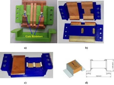
Fig. 10: Liquid cooler, where both top and bottom plastics are symmetric.
The liquid flows from the inlet toward the top cooling surface, and once it passes this surface, it turns down and flows via the bottom cooling area of the switch to get to the outlet. Rectangular gaskets were designed to seal the plastic and the switch cooling surface. Finally, the cooling system was assembled and fixed using screws.
3.3.
The connectors
Two connectors (Figure 11) are designed to connect the gate drive and load side of the assembly in order to have better accessibility and modularity. High frequency capacitors shown in Figure 8c are embedded into the load side connectors; the gate-driver connector is designed to embed the two gate resistors closer to both IGBTs. In the power connector two CeraLinkTM 1 μF-500 V low profile capacitors have been
embedded. The CeraLink is a family of capacitors specifically designed for fast switching 650 V semiconductors, offering new benchmark performances in terms of ratings, size and stability [12]. Here, only the liquid cooler is hermetically sealed and the other connectors are kept together by screws.
a) b)
c) d)
[image:7.595.101.494.448.739.2]3.1.DC-link, gate drive and load side PCB
The gate drive and power PCB boards are kept very close to the switch to minimize the noise pick up at the gate signals and parasitic inductances. Two electrolytic and high frequency capacitors are used to suppress the voltage oscillations at the DC bus. A dedicated test board was built which accommodates passives and interface with the control platform, where a fixed dead time of 0.5 μs was chosen. The general block diagram of the gate driver circuit, containing the FPGA control platform from Altera and a host PC, is depicted in Figure 12. Here a sinusoidal PWM is implemented to generate the required gate signals.
[image:8.595.150.446.235.414.2]Gate and power side PCBs are also designed taking into account that the connection with the HBS will be done by means of edge connectors.
Fig. 12: Two channels gate driver block diagram.
4.
Experimental test
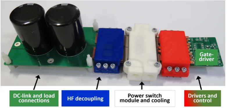
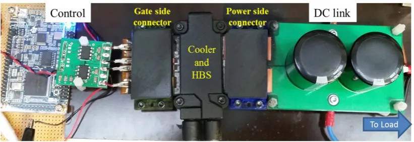
The whole setup shown in Figure 13 corresponds to the schematic diagram listed in Figure 1. The idea was to produce a plug-in system. This feature can help to reduce downtime and drive down maintenance costs of repairable systems. As it is shown in the figure, the whole system is a combination of control, switching, load and cooling along with the embedded capacitors and resistors into the customized connectors.
The assembled hardware and test setup of a single phase inverter was made mainly to test the performances of the HBS and the quick connectors. Preliminary functional tests were carried out in an open-loop system operating at 300 V DC input voltage and 10 kHz switching frequency having 30 Ω load resistance and 8.4 mH load inductance.
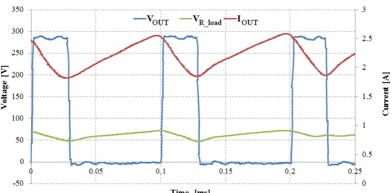
[image:8.595.71.482.593.734.2]Two LeCroy differential probes were used to measure the voltages across the switch and 30 Ω load resistor, and the corresponding results were observed in LeCroy oscilloscope. Figure 14 shows a current through the load, and three representative experimental results (zoomed in) are shown in Figure 15: voltage across load resistor (VR_load), current flowing through the load (IOUT) and voltage across the
[image:9.595.142.453.151.327.2]switch (VOUT) revealing a complete no overshoots.
Fig. 14: Experimental result: load current waveform.
Fig. 15: Representative preliminary test waveforms for the converter.
5.
Conclusions
[image:9.595.106.490.358.547.2]References
[1] B. C. Charboneau, F. Wang, J. D. Van Wyk, D. Boroyevich, Z. Liang, E. P. Scott, C. W. Tipton, “Double-Sided Liquid Cooling for Power Semiconductor Devices Using Embedded Power Packaging,” IEEE Trans. Ind. Appl., vol. 44, no. 5, 2008.
[2] “DENSO Develops High Output Power Control Unit and Battery Cooling System for Hybrid Vehicles.” DENSO news ref. N. D0705 05/31/2007, 2007.
[3] X. Cao, T. Wang, Z. Tan, K. Ngo, S. Luo, and G.-Q. Lu, “Development of a Double-side Cooled Power Module Joined by Low-temperature Sintering of Nanosilver Paste for Electric Vehicles,” in IMAPS’s 2nd Advanced Technology Workshop on Automotive Microelec. and Packaging, 2010.
[4] J. Marcinkowski, “Innovative CooliR2 TM Packaging Platform with Dual-side Cooling Advances HEVs and EVs,” Infineon technical paper.
[5] M. Schneider-Ramelow, “Design and assembly of power semiconductors with double-sided water cooling,” in 5th International Conference on Integrated Power Systems (CIPS), 2008, pp. 1-7.
[6] M. Meisser, D. Hamilton, T. Blank, P. Mawby, “Low - inductive compact SiC power modules for high - frequency operation,” in PCIM Europe 2014; International Exhibition and Conference for Power Electronics, Intelligent Motion, Renewable Energy and Energy Management, 2014, pp. 1-8.
[7] M. Schmenger, M. Meisser, D. Hamilton, B. Leyrer, M. Bernd, P. Mawby, T. Blank, “Highly integrated power modules based on copper thickfilmonDCB for high frequency operation of SiC semiconductors -design and manufacture,” in 18th European Conference on Power Electronics and Applications, 2015. [8] A. K. Solomon, A. Castellazzi, N. Delmonte, P. Cova, “Modular power Converter Integration Based On
Non-Conventional Power Switch Assembly and Interconnects”, Proc. 9th International Conference on Power Electronics, ICPE 2015-ECCE ASIA, Seoul, Korea, Jun. 1-5, 2015, pp. 837-843.
[9] “Engineering and operating guide for DOWFROST and DOWFROST HD inhibited propylene glycol-based heat transfer fluids”, The Dow Chemical Company, 2008.
[10]P. Cova, N. Delmonte, F. Giuliani, M. Citterio, S. Latorre, M. Lazzaroni, A. Lanza, “Thermal optimization of water heat sink for power converters with tight thermal constraints,” Microel. Reliab., vol. 53, pp. 1760-1765, 2013.
[11]R. Skuriat, C. M. Johnson “Direct Substrate Cooling of Power Electronics” Integrated Power Systems (CIPS), 2008 5th International Conference on Integration of Power Electronics Systems, Germany.