ISSN Online: 2153-120X ISSN Print: 2153-1196
Nitrogen Desorption and Positron Sensitive
Defect of CVD Diamond
Kasey R. Lund
1,
Kelvin G. Lynn
2,
Marc H. Weber
3, Chao Liu
4, Elgin Eissler
41National Superconducting Cyclotron Laboratory Michigan State University, East Lansing, MI, USA
2Center for Materials Research, Department of Physics, School of Mechanical and Materials Engineering, Washington State University, Pullman, WA, USA
3Center for Materials Research, Washington State University, Pullman, WA, USA 4II-VI Incorporated, Saxonburg, PA, USA
Abstract
The chemical vapor deposition (CVD) process can produce single or poly-crystalline diamond samples of high purity or with controlled doping concen-trations. The defect type in the CVD diamonds can be changed by heating the samples. Controlling the defect type can be used to create devices for quantum diamond switches that could be used in radiation sensors and quantum in-formation technology. Eight samples of CVD diamonds were analyzed with Doppler broadening of positron annihilation radiation (DBAR) before and after annealing in high vacuum with an electron gun. Between temperatures of 1700 - 1850 K, nitrogen was liberated from the diamond sample. At these high temperatures, the surface was graphitized and a change in the color and transparency of the diamond was observed. Some of the samples were ana-lyzed with DBAR during periods with and without light. The defect properties were observed to change depending on the time exposure to the positron beam and were then regenerated by exposure to light. The DBAR data is compared to photoluminescence data and a time varying defect state is dis-cussed for detector and optical grade type II CVD diamonds.
Keywords
CVD Diamond Detectors, Positron Annihilation Spectroscopy, Divacancy
1. Introduction
Much attention has been giving to CVD diamonds because of their electrical and
mechanical properties. Previous work [1][2][3] has shown that CVD diamonds
can be manipulated to tune their properties in order to create devices for quan-tum mechanical diamond switches that could be used in diamond sensors,
io-How to cite this paper: Lund, K.R., Lynn, K.G., Weber, M.H., Liu, C. and Eissler, E. (2017) Nitrogen Desorption and Positron Sensitive Defect of CVD Diamond. Journal of Modern Physics, 8, 770-785.
https://doi.org/10.4236/jmp.2017.85049
Received: March 9, 2017 Accepted: April 22, 2017 Published: April 25, 2017
Copyright © 2017 by authors and Scientific Research Publishing Inc. This work is licensed under the Creative Commons Attribution International License (CC BY 4.0).
nizing radiation detectors, spintronics, quantum computing applications, and other quantum information technology applications.
A majority of the work done on diamond defects has been focused on the NV center [4]-[10] while little attention was given to the divacancy [11] [12] [13]
[14][15]. It has been shown that monovacancies in diamonds will migrate to
ni-trogen impurities when annealed at temperatures between than 800 - 1050 K
[16][17] [18] with a migration energy of 2.2 ± 0.2 eV [18]. During annealing,
existing negatively charged monovacancy (V−) are converted to the neutral
charged monovacancy (V0), then, the V0 migrates to, and is trapped by, any
ni-trogen impurities creating the NV center [19]. The NV center can be neutral (NV0) or negatively charged (NV−). Beha et al. [6] have shown that the NV0
charge state is present in the absence of light and can be changed to the NV− by
shining light on the sample. Positron annihilation spectroscopy has shown a de-cay time constant believed to be related to the NV center [7] but is not well un-derstood. It is also reported that prolonged annealing above 1100 K will produce the divacancy (V2) defect [14][15].
In this study, we characterized the effects of annealing CVD diamond samples with the aim of desorbing any nitrogen impurity atoms and then further an-nealing to create divacancies without destroying or graphitizing the diamond samples. The diamonds were analyzed using Doppler broadening of positron annihilation radiation (DBAR) to observe defect changes as a function of an-nealing.
We were able to heat the CVD diamond samples to release nitrogen and we observed a time dependent change of the defect state within the diamond sam-ples during positron annihilation. This change can be regenerated by shining light on the sample. In the following manuscript we will show the temperatures required to desorb nitrogen from CVD diamonds. We will then discuss our ob-servations regarding the implantation of a positron near the light sensitive defect and compare to previously reported observations.
2. Methods
2.1. Heating Procedure
Eight polycrystalline CVD diamond samples were provided from II-VI Inc. The samples were mounted to a tantalum support holder and suspended from an ul-tra-high vacuum and high voltage feed through. For each sample, the vacuum
system was evacuated and baked until the base pressure was 5 × 10⁻⁹ Torr. An
ion pump was used to maintain vacuum during heating. An electron-gun
(e-gun) with a thoriated tungsten filament 0.125 mm diameter was positioned
approximately 2 cm from the sample. The sample and tantalum holder were bi-ased with a positive high voltage source to attract the electrons to it. The e-gun
was grounded and heated using an AC power source.
diamond and viewed the samples temperature through a quartz view port. Temperatures lower than 650 K were extrapolated from a fitting curve of the power required to heat the sample. A Stanford Research Systems Residual Gas Analyzer (RGA) 100 was used to record the partial pressures of the expelled gasses while a nude ion gauge was used to measure the total pressure of the va-cuum system.
In preparation of heating the samples, the e-gun filament was turned on with
1.5 Amps AC for approximately 24 hours. This was found to help stabilized the
emission current from the filament during heating operations and helped to mi-nimize temperature fluctuations of the sample. The first four samples (labeled
A-D) were heated at an average rate of 12 ± 3 K/min until nitrogen desorption
was observed and then cooled to room temperature at an average rate of 32 ± 12 K/min.
The second four samples (labeled E-H) were heated by increasing the target
bias and the emission current of the e-gun every 30 mins until a desired
temper-ature was achieved. These samples were detector grade and optical grade sam-ples that had two different surface treatments. The first being a mechanical polish method and the second being a reactive ion etching (RIE) method. It is believed that surface conditions will affect the quality of a diamond being used as a radiation detector. This is why two different polishing methods were employed in our study.
The values of the emission current, bias voltage, and recorded or extrapolated
temperatures for the latter four samples are displayed in Table 1. Once the
de-sired temperature was achieved, the temperature was held constant. After 24 hours at a constant temperature, the samples were cooled to room temperature
by turning the e-beam off. They remained in vacuum for 30 mins before the
[image:3.595.208.538.514.724.2]sys-tem was vented with dry nitrogen gas.
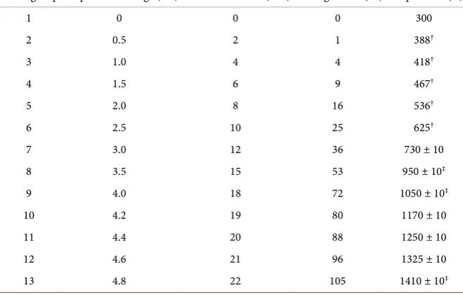
Table 1. Heating profile of CVD diamond samples E-H.
Heating Step Sample Bias Voltage (kV) Emission Current (mA) Heating Power (W) Temperature (K)
1 0 0 0 300
2 0.5 2 1 388†
3 1.0 4 4 418†
4 1.5 6 9 467†
5 2.0 8 16 536†
6 2.5 10 25 625†
7 3.0 12 36 730 ± 10
8 3.5 15 53 950 ± 10‡
9 4.0 18 72 1050 ± 10‡
10 4.2 19 80 1170 ± 10
11 4.4 20 88 1250 ± 10
12 4.6 21 96 1325 ± 10
13 4.8 22 105 1410 ± 10‡
For all heating runs, the tantalum support holder was heated with no sample to measure any background gases for each temperature profile. This blank tan-talum data was subtracted from the CVD diamond heating data and the amount
of gas above this recorded background (5 × 10⁻¹¹ Torr) is reported below. Table
2 lists all the samples used and descriptive information. Also, shown in Table 2
is the bulk value of the S-parameter after its annealing temperature and time.
2.2. DBAR with and without Light
The variable energy monoenergetic positron beam at Washington State Univer-sity (WSU) was used to probe the samples for vacancies and other open volume type defects. The technique is sensitive to neutral and negatively charged defects. Following implantation at a mean depth determined by the incident kinetic energy of the positrons, the positrons thermalized within several picoseconds. The positrons diffuse throughout a volume on the order of 106 lattice sites.
Upon encounter with a vacancy (or larger defect) the positron is trapped in the attractive potential well created by the missing atom and valence and con-duction electron bands extending into this volume. After lifetimes of typically several 100 picoseconds the positrons annihilate either from the trap, with pre-dominantly low momentum electrons, or from core electrons with higher mo-mentum distributions.
The emitted annihilation photons carry information on the annihilation sites as changes in their Doppler shifts due to the electron momentum. In a typical experiment 1 to 2 million annihilation events are acquired. The Doppler broa-dened annihilation line shape is parameterized into a shape (S) and a wings (W) parameter to reflect changes in the open volume defect concentration and size
[image:4.595.58.539.493.721.2](S) and the chemical environment (W) of the defects combined with an inverse
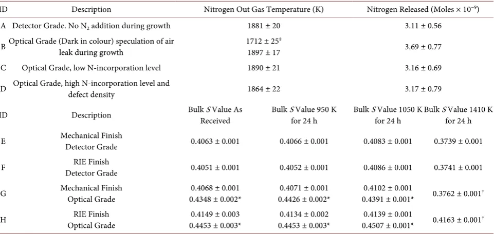
Table 2. Sample information.
ID Description Nitrogen Out Gas Temperature (K) Nitrogen Released (Moles × 10−9)
A Detector Grade. No N2 addition during growth 1881 ± 20 3.11 ± 0.56
B Optical Grade (Dark in colour) speculation of air leak during growth 1712 ± 251897 ± 17 ‡ 3.69 ± 0.77
C Optical Grade, low N-incorporation level 1890 ± 21 3.16 ± 0.69
D Optical Grade, high N-incorporation level and defect density 1864 ± 22 3.17 ± 0.79
ID Description Bulk S Value As Received Bulk S Value 950 K for 24 h Bulk S Value 1050 K for 24 h Bulk S Value 1410 K for 24 h
E Mechanical Finish Detector Grade 0.4063 ± 0.001 0.4066 ± 0.001 0.4083 ± 0.001 0.3739 ± 0.001
F Detector Grade RIE Finish 0.4051 ± 0.001 0.4052 ± 0.001 0.4086 ± 0.001 0.3741 ± 0.001
G Mechanical Finish Optical Grade 0.4348 ± 0.002* 0.4068 ± 0.001 0.4426 ± 0.002* 0.4071 ± 0.001 0.4391 ± 0.001* 0.4102 ± 0.001 0.3762 ± 0.001†
H Optical Grade RIE Finish 0.4453 ± 0.003* 0.4149 ± 0.003 0.4453 ± 0.003* 0.4134 ± 0.002 0.4507 ± 0.001* 0.4139 ± 0.001 0.4163 ± 0.001†
concentration and size effect.
The mean implantation depth of the positrons can be varied by tuning their incident kinetic energy. The mean depth is calculated with the empirical formula
[21],
1.6
40
z E
ρ
= . (1)
In this equation, ρ is the density in g/cm3 (3.52 g/cm3 for CVD diamond) and
E is the energy of the positron beam in keV (up to 70 keV for our system). This
way z will carry units of nm resulting in a maximum mean implantation of
10.18 µm at 70 keV.
Doppler broadening of positron annihilation radiation (DBAR) was per-formed before and after each heating phase at room temperature. By varying the positron beam energy, one is able to probe the surface to the bulk of the sample and create a defect profile for the sample. Conservation of momentum and energy leads to a Doppler shift of the annihilation gamma emission of the elec-tron posielec-tron pair. The 511 keV annihilation peak in the gamma spectra will be
changed depending on the type and concentration of defects. The S and W
pa-rameters, mentioned above, are used for this work and are described in further detail in References [20][21][22].
The vacuum chamber used to measure the annihilation spectrum is con-structed so that no visible light can shine inside the chamber. The CVD diamond samples were exposed to sunlight and laboratory light while they were taken from the annealing vacuum chamber and mounted to the positron beam va-cuum chamber. A small LED was mounted inside the vava-cuum chamber to shine light on the samples after they had reached a stable state while being exposed to positron.
3. Results
3.1. Annealing and Positron Analysis
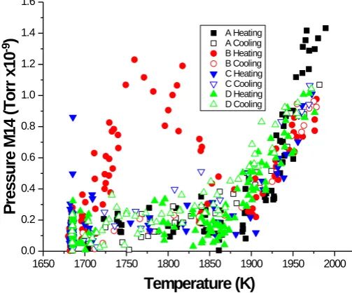
For the first four samples of CVD diamonds, the heating profile (heated at 12 ± 3 K/min then cooled at 32 ± 12 K/min) was created with the aim of finding what temperature is needed for a detectable amount of nitrogen to be liberated from
the sample. Figure 1 shows the interpolated data between the RGA and
pyro-meter from heating and cooling of the first four samples. All of the samples show an increase in the amount of detected nitrogen at a temperatures between 1850 - 1900 K.
Only one sample shows an early release of nitrogen near 1700 K. The reason for this early release is not yet fully understood but could be due to the fact that this sample was grown with a leak in the vacuum system and contains more ni-trogen and nini-trogen defects because of the leak.
In the cracking pattern of the RGA, mass 28 is the primary peak observed for
N2 gas. This is also the primary peak for carbon monoxide and the most intense
secondary peak of CO2. To distinguish between the gasses, masses 14 for
Figure 1. Nitrogen outgas vs. temperature for samples A-D. For the first four samples of CVD diamonds, we see that nitrogen is released between 1850 and 1900 K according to the partial pressure of mass 14. Sample B shows a release of nitrogen at lower tempera-tures compared to the other samples. This is most likely due to the fact that this sample had a higher amount of nitrogen caused by what was presumed to be an air leak during growth.
28 rises, mass 14 rises with the correct cracking pattern ratio that is expected for
nitrogen (M28 = 100%, M14 = 7.2%). At this time mass 12 did not rise. This
in-dicates that there is no measurable carbon monoxide coming out of the CVD samples for the detection limits used and that the measured amount of mass 14 is 7.2% of the amount of nitrogen being expelled from the sample. Mass 40 and 20 were seen to rise above the background measurements at these times sug-gesting that argon was being expelled from the samples as well. Besides mass 2 for hydrogen, no other masses (between 1 and 48) were observed to rise at these temperatures for the four samples measured above background of the RGA (5 × 10⁻¹¹ Torr).
Figure 2 shows the initial photoluminescence response before heating the first four samples. All but the detector grade diamond samples show a significant peak at 575 nm that is correlated with the neutral nitrogen-vacancy (NV0) defect
center. Some of the samples show a broad defect peak between wavelengths of 600 - 800 nm. Within these wavelengths are the signatures for other defects such as the divacancy (590, 614, 649, 674, and 685 nm) [23].
As stated previously, DBAR data was taken before and after heating of the
samples. Figure 3(a) shows the DBAR data before the samples were heated vs.
the intensity of the photoluminescence peak associated with the NV center. Figure
3(b) shows the change in the DBAR S-parameter as a function of the amount of
nitrogen that was liberated from the sample. The dashed line in both graphs is to guide the eye and show the linear relationship between the two measured quan-tities. From this we postulate that the initial bulk defects must be linked to the
NV center and that the amount of nitrogen released from the samples creates
1650 1700 1750 1800 1850 1900 1950 2000 0.0
0.2 0.4 0.6 0.8 1.0 1.2 1.4 1.6
A Heating A Cooling B Heating B Cooling C Heating C Cooling D Heating D Cooling
P
ressu
re M
14
(Tor
r x
1
0
-9
)
Figure 2. Photoluminescence response for the first four samples before annealing. Sam-ple A is in black, B is in red, C is in blue, and D is represented by green.
(a) (b)
Figure 3. (a) Normalized S parameter data vs. photoluminescence of the NV center. These data are taken before heating the sam-ples and shows a least square fit to the data indicates a linear correlation between the S parameter and the PL intensity. The
S-parameter was normalized to the bulk value of a single crystal sample from GE. (b) Normalized S parameter vs. Nitrogen outgas for samples A-D. The change in the S-parameter increases with the amount of nitrogen released while the W-parameter remained the same or only slightly increased. The S-parameter was normalized to the bulk value of a single crystal sample from GE.
more or larger defect (such as a divacancy) as indicated by the increase in the
S-parameter.
It is well-known that CVD diamonds can contain large vacancy clusters. Our
PL data suggests that the samples we examined did not contain a measurable
amount of large vacancy clusters to begin with.
The second set of samples were detector grade and optical grade with two
dif-ferent surface finishes (see Table 2 for more information). The optical grade
samples show a difference in the measured DBAR data depending on what side was being measured. The growth side of the optical samples showed a lower bulk
S-parameter than the substrate side. The detector grade samples did not show a
significant difference between the growth and substrate sides. Figure 4 shows
the S-parameter normalized to the bulk value of high purity single crystal as a
0.0 0.3 0.6 0.9 1.2 1.5 1.8
1.00 1.02 1.04 1.06 1.08
0.090 0.088 0.086 0.084 0.082 0.080
D B
S-Parameter
S/
SG
E
=
0.
40662
PL intensity at 575 nm (a.u.) A
C
W-Parameter
W
3.1 3.2 3.3 3.4 3.5 3.6 3.7
0.006 0.008 0.010 0.012 0.014 0.016 0.018 0.020
∆
S/
SG
E
=
0.
40662
Total N2 Gas (10-9 Moles)
B
C D
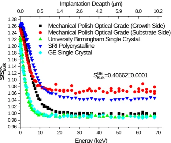
[image:7.595.64.533.277.473.2]Figure 4. Normalized S parameter vs energy for the mechanical polished optical grade growth and Back side along with single crystal CVD diamond from the university of Bir-mingham and an SRI polycrystalline diamond sample.
function of the mean positron implantation depth. To compare the growth and substrate side of the sample along with a polycrystalline sample from the Stan-ford Research Institute (SRI), a single crystal sample with a low defect concen-tration from the University of Birmingham, and a single crystal sample from
General Electric (GE). The Bulk S value from the GE sample was used to
nor-malize the rest of the data and has a value of 0.40662 ± 0.0001.
As stated above, Lawson has shown that monovacancies in diamonds will be-come mobile at 900 K. Davis and Pu report that between 900 - 1050 K the mo-novacancies, if charged, become neutral and migrate to and become trapped at
nitrogen impurities creating the NV defect. Above 1100 K Twitchen and
Stes-man report that divacancies will be produces. With this information in mind, we chose to anneal the second set of samples first at 950 K, then at 1050 K and fi-nally at 1410 K.
The heating profiles were created so we could use the DBAR technique to ob-serve the differences between the as received sample, after heating to 900 K to allow the vacancies to migrate to nitrogen impurities, then after heating to 1050 K to see the changes made by forming the NV−/0 center, and finally after heating
to 1410 K to create divacancies.
Figure 5 shows that heating to 950 K for 24 hours only slightly increased the S-parameter in all samples except for one of the optical grade samples. This sample had the largest initial value of the S-parameter, indicating more defects, divacancies, or larger open volume between grain boundaries. Heating at 950 K could have caused a reduction in the number of defects. After annealing at 1050 K for 24 hours, all samples showed a significant increase in the bulk S-parameter by roughly 0.5%.
0 10 20 30 40 50 60 70
0.96 0.98 1.00 1.02 1.04 1.06 1.08 1.10 1.12 1.14 1.16 1.18 1.20 1.22 1.24 1.26 1.28
SGEBulk=0.406620.0001
Mechanical Polish Optical Grade (Growth Side) Mechanical Polish Optical Grade (Substrate Side) University Birmingham Single Crystal
SRI Polycrystalline GE Single Crystal
S/
S
GE Bu
lk
Energy (keV)
0.0 0.5 1.4 2.6 4.2 5.9 8.0 10.2
After the 1410 K 24 hour anneal, all of the samples except the RIE finished optical grade sample show a large drop of approximately 8% in the S-parameter. The RIE finished optical grade sample instead shows and increase in the
S-parameter by about 0.6%. The reason for the difference in behavior for this
[image:9.595.244.501.218.418.2]sample is not fully understood.
Figure 6 shows the S vs W DBAR parameters for all four samples with the
different annealing temperatures represented by different colors and the bulk S
and W values for the two crystal diamond from the University of Birmingham
[image:9.595.246.502.476.679.2]and a diamond from GE. There is a single slope indicating only one defect type
Figure 5. Normalized S parameter vs. annealing temperature for samples E-H. These data were measured at room temperature after sample heating. Heating for 24 hours up to 1400 K did not release any nitrogen above background levels.
Figure 6. Normalized S parameter vs W plots. Shown here are all the S and W data for the second four samples with the color indicating what temperature the samples were annealed at. A single slope on the SW plot suggests one type of defect throughout the measured depth. Different slopes indicate different defect types.
300 400 500 600 700 800 900 1000 1100 1200 1300 1400 0.92
0.94 0.96 0.98 1.00 1.02
E F G H
S/
S
GE Bu
lk
Annealing Temperature (K)
A
s R
ec
ei
ved
0.04 0.05 0.06 0.07 0.08 0.09 0.10
0.90 0.95 1.00 1.05 1.10 1.15 1.20 1.25
1.30 As Recieved
900K
1050K 1410K
Bulk value Single Crystal from U. Birmingham
Bulk value Single Crystal from GE
S
/S
GE Bu
lk
W Surface
for each annealing temperature. The surface state is located at higher S and low-er W values (top left) on the graph and the bulk state is located at lower S and
Higher W values (bottom right) on the graph. The bulk values of the second
diamond set is similar to the single crystal sample from GE and the single crystal
sample from the University of Birmingham has a similar bulk S value but a
higher bulk W value.
The slope of the S vs. W plot changes for different annealing temperatures.
For temperatures of 900 K and 1050 K, the slope is only slightly decreasing for the surface states. This suggests the surface defect type is slowly changing with
increasing annealing temperature. After the 1410 K annealing, the SW slope
radically changes suggesting the defect type is completely different. 1410 K is the temperature where we expected to see divacancies created.
If this were true, we would expect to see nitrogen desorb from the samples in the RGA data. However, we were unable to detect any nitrogen above
back-ground levels. Furthermore, the divacancies should have a higher S and lower W
value than the low temperature annealed samples because the divacancy is a
larger defect than the single vacancy and the S-parameter is a measure of defect
size and concentration. Also, the bulk values for S and W for the two crystal
sample should be the lowest S and highest W, but we see from the S vs. W plot this is not the case.
3.2. Time Changing of the Vacancy State with Positron
Annihilations and Photons
All of the samples are sensitive to visible light. The S data decay gradually with time while the sample is in the dark. Exposure to red, green or blue LED light
(10 mA of a typical low power LED suffices) restores the initial higher S value.
The decay has at least two lifetimes of 15 to 30 minute and a longer one of
sever-al hours. Figure 7 shows typical data for an optical grade diamond sample after
annealing at 1450 K for 85 min. The excitation with light appears to be much faster than the typical positron measurement time of 1 to 10 minutes per
da-ta-point and is independent of photon energy (red to blue and near UV). The
data are consistent with electrons being photo-excited into defects above the Fermi level near the middle of the band-gap. The excited states are long lived (>> hours) with electrons being removed by annihilation with positrons. The change in charge of the defect from neutral (or positive) when empty to negative (or neutral) when illuminated causes a change in the positron signal.
Implanting positrons first at 28 keV (2.3 µm mean depth) to deplete the ex-cited states and then after several hours of exposure changing the implantation depth to 44 keV (4.8 µm) shows that the defects at that depth are still excited and only decay once positrons can reach this depth. Furthermore, the magnitude of the light-effect is related to the bulk S value in the sample, in that it increases with increasing S, i.e. it is tied to the defect observed in the dark.
The temperature and light dependence was also tested on the SRI sample (See
Figure 7. II-VI batch 3 OPTICAL grade 1450 K anneal for 85 min, short term decay measurement (1 min/data point, repeated several times) at a positron implantation ener-gy of 28 keV (2.3 um depth). The green line is an 11 point average of the black data points, and the red line is an exponential fit of the data the gives a time constant of 17.2 ± 3.3 mins.
Figure 8. SRI sample growth side, temperature dependent positron measurements in dark or with light (blue 470 nm). Values were normalized to the samples starting bulk value for the S-parameter of 0.40103 ± 0.00015.
temperature range at approximately the mid-level. Turning the light off causes S
to increase by 3%. Allowing the sample to cool lowers the S value to the previous
room temperature value as shown in light green points on Figure 8.
Measuring in the dark during increasing temperatures, S increases about 6%
between 425 and 525 K. This process reverses upon cooling back to room tem-perature as shown in dark green points. Turning a 470 nm LED light on after
heating to and holding at 565 K, lowers S to the “light on” level. Here the mid
0.0 0.5 1.0 1.5 2.0
0.394 0.396 0.398 0.400 0.402 0.404 0.406 0.408 0.410 0.412 0.414 0.416
Exp. decay: S(t) =
χ2
/DoF = 0.43804;
Sdark = 0.40329±0.0
S470nm = 0.40904±0
τ1/2 = 17.18±3.27 m Blue light 470nm, 30.1±0.1mA off at t = 0min
S for ∆t = 64.51±0.35 sec S from 11-pts running average
S from exp. decay fit; τ1/2 = 17.2±3.3min
S
Time in dark (hrs Time in Dark (h)
Data
11-pts Average
Decay Fit:τ= 7.2±3.3min
300 350 400 450 500 550 600
1.00 1.02 1.04 1.06 1.08 Li ght O n
1. Heating Light On
2. Cooling Light Off
3. Heating Light Off
4. Hold Temperature Light On
5. Cooling Light Off 2nd
[image:11.595.238.506.355.573.2]gap defects are filled thermally in the dark and emptied by photo-excitation into the conduction band at high temperature.
Wotherspoon et al. [7] reported a DBAR relaxation time for diamond samples
that were doped with nitrogen. They report that the S-parameter of the diamond
sample would change by as much as 2% when illuminated with light. Then, after
hundreds of hours, the original value of the S-parameter is recover by a slow
de-cay process. In their manuscript they state that the strongest effects occur for the higher nitrogen doped diamonds. They were able to determine that this effect is
not due to ionizations of the NV− center by observing this effect with a light
source unable to cause ionization.
We have observed a similar behavior with our diamond samples. Our samples were exposed to ambient sunlight and laboratory florescent lights. In the posi-tron beam vacuum chamber, they were mounted in darkness. Once they were
exposed to positrons, the S-parameter in the bulk of the sample would decay to a
lower value in a matter of minutes. Depending on the annealing temperature, the time constant from the exponential decay fit varied between 20 - 90 min.
Then, when the sample is illuminated with light, the S-parameter jumps back up
to the starting value of the S-parameter. The light source used was a 470 nm LED
operated at 20 - 30 mA. Note the absolute photon flux, the LED current, and
LED positon had no discernible effect. The illumination caused the S-parameter
to regenerate instantaneously.
For our measurement acquisition times (less than 1 - 3 min), we are unable to
determine the regeneration time. Figure 9(a) shows the decay of the
S-parameter for one sample which contained a higher bulk S-parameter after
annealing at 1050 K. These data were fit with an exponential decay function and
[image:12.595.66.533.467.677.2](a) (b)
Figure 9. (a) Bulk S-parameter decay with time while being exposed to a positron beam at 20 keV. Black squares are the measured data points and the red line is the exponential decay fit. This data was taken at room temperature after the sample was heated past 1050 K for 24 hours. (b) Time constant of the defect decay vs. the sample annealing temperature. The black squares are the values obtained at room temperature from the DBAR data using the fitting equation and the dashed line is to guide the eye.
0 50 100 150 200 250
0.410 0.415 0.420 0.425 0.430 0.435 0.440
Sbul
k
Time After Light Off(min)
Model ExpDec1
Equation y = A1*exp(-x/t1) + y0
Plot S
y0 0.41766
A1 0.01822
t1 69.25529
Reduced Chi-Sqr 0.39342 R-Square(COD) 0.82402 Adj. R-Square 0.8225
200 400 600 800 1000 1200 1400
0 10 20 30 40 50 60 70 80 90 100 110
RIE Optical Grade
TI
me C
ons
tant
(m
in)
the time constant of the decay was (69.3 ± 6.1) min for this particular annealing
temperature. The change in the time constant is plotted in Figure 9(b) as a
function of annealing temperature for the RIE optical grade sample.
Our findings support Wotherspoon et al. in that we see a change in the defect
state with the illumination of light, we see a time decay in the DBAR data when the sample is in the dark, and we also report about a 2% change in the
S-parameter during this light and dark switching. However, our relaxation times
are much shorter than the time reported by Wotherspoon et al. This could be
due to the differences in beam intensities. We are unsure as Wotherspoon did not report the positron flux, however, our system was set up so that positrons
from a 22Na source would produce 1642 ± 15 cps in the 511 keV photo peak as
detected by an HPGe gamma detector.
4. Discussion and Conclusion
Eight CVD diamond samples were annealed at high temperatures and analyzed with DBAR and PL techniques. The first set of four samples released nitrogen at temperatures above 1850 and 1900 K. The spread in desorption temperature could be due to slight differences with the time required to reach the annealing temperature.
We have shown a linear dependence between the increase in the S value and
the amount of nitrogen released for these four samples. This would suggest that the expelled nitrogen leaves vacancies in their place, hence the rise in the S value.
PL data show a correlation with the NV center and the S-parameter. These
samples showed surface graphitization and were darker in color. This is possibly
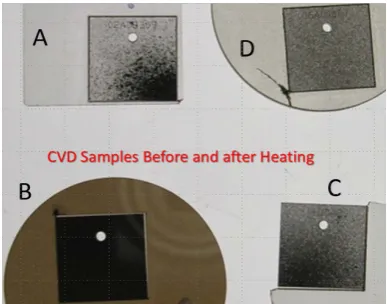
due to vacancy cluster forming in the samples. Figure 10 show a photograph of
[image:13.595.276.470.515.667.2]these samples before and after annealing to high temperatures. The black dots are surface graphitization. At the moment we do not fully understand if there is a correlation between surface graphitization and the amount of nitrogen that was released.
The second set of four samples were created to have low nitrogen levels and low defect concentration. They were annealed to cause the vacancies (if any ex-isted) to migrate to the surface and become trapped at any nitrogen impurity sites. Isochronal annealing of the samples shows that after 1050 K the
S-parameter is increased, this is the temperature where we expected to see an
in-crease in the number of NV−/0 centers.
Annealing the samples above 1400 K, was expected to create divacancies in the place of the NV−/0 center. This idea is supported by the fact that the SW slope is
radically different from the lower temperature annealing, although not as we
predicted. As stated above, the SW slope can be used as an indication of the
de-fect type with different dede-fects having different SW slopes. As we see from
Fig-ure 6, annealing the samples from the as received state to 900 K and 1050 K started to change the surface defect of the samples. Then after the 1400 K an-nealing, the S vs. W slope has radically changed indicating that the defect type has changed as well. According to the literature, this is the temperature that
would create divacancies by liberating the nitrogen atom from the NV defect.
However nitrogen desorption was not detected above our background signal
in the RGA and the S vs. W plot does not support the claim that this annealing
temperature creates divacancies. Furthermore, the PL data did not show clear
signs of an increase of divacancies. After the 1410 K anneal for 24 hours, the samples are only slightly darker in color and do not show signs of graphitization on the surface. It is possible that this annealing method produced vacancy clus-ters and not divacancies.
During heating of the CVD diamonds, the surface temperature gradients measured by the pyrometers were as high as 100 K, therefore, the temperature measurements were sensitive to the positioning of the pyrometers. This effect was minimized by focusing on the sample center which was the hottest spot during heating. This also introduces an error in all of the temperature measure-ments to be added to the error by measuring through a quartz window.
The observed positron induced time constant ranges between 10 - 100 mins for the samples to reach stability when the samples are exposed to positrons in
the dark. This can be explained by the NV center changing from the negative
state, with a metastable electron, to a neutral state when the positron annihilates the metastable electron. Then when light shines on the diamond, the photon
causes an electron to populate the metastable state and the neutral NV center
now becomes negative and the S-parameter is increased.
The samples time changing effects were strongly observed with samples that
had an initially higher value of DBAR S-parameter. This supports the
observa-tion that the time changing effects are only observed in the defect centers.
Further studies are needed where PL or Raman spectroscopy is used to more
accurately measure the amount of NV and V2 defects before and after the
By changing the positron flux, and measuring the decay constant we would be able to determine if the positrons are annihilating a metastable electron in the defect. Measuring for shorter acquisition times with a higher positron flux would allow us to measure the regeneration time.
Acknowledgements
The authors would like to acknowledge Klaas Monster and Chandra Minnal for their assistance in the lab.
References
[1] Aslam, N., Waldherr, G., Neumann, P., Jelezko, F. and Wrachtrup, J. (2013) New Journal of Physics, 15, Article ID: 013064.
https://doi.org/10.1088/1367-2630/15/1/013064
[2] Jelezko, F. and Wrachtrup, J. (2006) Physica Status Solidi, 203, 3207-3225. https://doi.org/10.1002/pssa.200671403
[3] Aharonovich, I., Greentree, A.D. and Prawer, S. (2011) Nature Photonics, 5, 397- 405. https://doi.org/10.1038/nphoton.2011.54
[4] Meijer, J. and Burchard, B. (2005) Applied Physics Letters, 87, Article ID: 2619909. https://doi.org/10.1063/1.2103389
[5] Khan, R.U.A., Martineau, P.M., Cann, B.L., Newton, M.E. and Twitchen, D.J. (2009) Journal Physics: Condensed Matter, 21, Article ID: 364214.
https://doi.org/10.1088/0953-8984/21/36/364214
[6] Beha, K., Batalov, A., Manson, N.B., Bratschitsch, R. and Leitenstorfer, A. (2012)
Physical Review Letters, 109, Article ID: 097404. https://doi.org/10.1103/PhysRevLett.109.097404
[7] Wotherspoon, A., Steeds, J.W., Catmull, B. and Butler, J. (2003) Diamond and Re-lated Materials, 12, 652-657.
[8] Sachdeva, A., Sudarshan, K., Pujari, P.K., Goswami, A., Sreejith, K., George, V.C., Pillai, C.G.S. and Dua, A.K. (2004) Diamond and Related Materials, 13, 1719-1724. [9] Maki, J.M., Tuomisto, F., Kelly, C., Fisher, D. and Martineau, P. (2007) Physica B:
Condensed Matter, 401-402, 613-616.
[10] Tang, Z., Chiba, T., Nagai, Y., Inoue, K., Toyama, T. and Hasegawa, M. (2014) Ap-plied Physics Letters, 104, Article ID: 172101. https://doi.org/10.1063/1.4872243 [11] Fujii, S., Nishibayashi, Y., Shikata, S., Uedono, A. and Tanigawa, S. (1995) Journal
of Applied Physics, 78, 1510-1513. https://doi.org/10.1063/1.360242
[12] Dannefaer, S., Zhu, W., Bretagnon, T. and Kerr, D. (1996) Physical Review B, 53, 1979-1984. https://doi.org/10.1103/PhysRevB.53.1979
[13] Pu, A., Avalos, V. and Dannefaer, S. (2001) Diamond and Related Materials, 10, 585-587.
[14] Stesmans, A., Nouwen, B. and Iakoubovskii, K. (2000) Journal of Physics: Con-densed Matter, 12, 7807-7817. https://doi.org/10.1088/0953-8984/12/35/315 [15] Twitchen, J., Newton, M.E., Baker, J.M., Anthony, T.R. and Banholzer, W.F. (1999)
Physical Review B, 59, Article ID: 12900. https://doi.org/10.1103/PhysRevB.59.12900
[17] Lawson, S., Davies, G., Collins, A.T. and Mainwood, A. (1992) Journal of Physics:
Condensed Matter, 4, L125-L131. https://doi.org/10.1088/0953-8984/4/9/001 [18] Davies, G., Lawson, S.C., Collins, A.T., Mainwood, A. and Sharp, S.J. (1992)
Physi-cal Review B, 46, Article ID: 13157. https://doi.org/10.1103/PhysRevB.46.13157 [19] Davies, G. and Collins, A.T. (1993) Diamond and Related Materials, 2, 80-86. [20] Schultz, P.J. and Lynn, K.G. (1988) Review of Modern Physics, 60, 701.
https://doi.org/10.1103/RevModPhys.60.701
[21] Siegel, R.W. (1980) Annual Review of Materials Science, 10, 393-425. https://doi.org/10.1146/annurev.ms.10.080180.002141
[22] Seidman, D.N. and Balluffi, R.W. (1965) Physical Review, 139, Article ID: A1824.
https://doi.org/10.1103/physrev.139.a1824
[23] Iakoubovskii, K. and Adriaenssens, G.J. (2000) Physical Review B, 61, Article ID: 10174. https://doi.org/10.1103/PhysRevB.61.10174
Submit or recommend next manuscript to SCIRP and we will provide best service for you:
Accepting pre-submission inquiries through Email, Facebook, LinkedIn, Twitter, etc. A wide selection of journals (inclusive of 9 subjects, more than 200 journals)
Providing 24-hour high-quality service User-friendly online submission system Fair and swift peer-review system
Efficient typesetting and proofreading procedure
Display of the result of downloads and visits, as well as the number of cited articles Maximum dissemination of your research work
Submit your manuscript at: http://papersubmission.scirp.org/