Synthesis and Analysis of PZT Using Impedance
Method of Reactance Estimation
Witsarut Sriratana1, Riichi Murayama1, Lerdlekha Tanachaikhan2
1Department of Intelligent Mechanical Engineering, Faculty of Engineering, Fukuoka Institute of Technology, Fukuoka, Japan 2Faculty of Engineering, Ramkhamhaeng University, Bangkok, Thailand
Email: [email protected], [email protected], [email protected]
Received January 28, 2013; revised February 16, 2013; accepted February 25, 2013
ABSTRACT
This study presents an analysis of equivalent circuit namely Butterworth Van Dyke (BVD) [1,2] by using impedance method to stimulate Zirconate Titanate (Piezoelectric ceramic) which is initially synthesized from Lead Oxide (PbO), Zirconium Dioxide (ZrO2) and Titanium Dioxide (TiO2) and vibrated in thickness mode. The reactance was estimated
in the frequency range lower than the resonance frequency and then compared to the impedance obtained from meas- urement using impedance analysis machine model HP4192A and HP4194 [3]. The results from HP4194 were analyzed for BVD parameters: Motional resistance (R1), Inductor (L1), Capacitor (C1), and Capacitor corresponds to the electro-
static capacitance (Co). Another accuracy analysis was compared by the calculation results using the method of IEEE 176-1987 [4] to the impedance values measured by HP4192A. In this study, there were two conditions for experiment and consideration of parameter variation in BVD equivalent circuit: variation of temperature and mechanical force. These parameters are evaluated to design the efficient circuit for PZT utilization to obtain the optimal efficiency.
Keywords: BVD; Capacitance; Force; Frequency; Impedance; Inductance; PZT; Temperature
1. Introduction
Electronic circuit using BVD analysis for effectively stimulating PZT can be designed by adopting, for exam- ple, IEEE Standard [4,5], Smits [6], Sherrit [7], and Xu [8]. Smith’s method and Sherrit’s method would con- sider those parameters as complex numbers. Xu’s method would be similar to Smith’s method which considers the impedance of piezoelectric measured at the frequency values ranging from resonance frequency (fr) and anti- resonance frequency (fa) as well as under mechanical force i.e. elastic, piezoelectric constant and coupling co- efficient. In this study, five pieces of PZT, namely O01, N01, N02, N03, and N04, were synthesized fromratio of PbO:ZrO2:TiO2 (100:52:48) and burned at 700˚C for 1
hour [9,10] in order to experiment the density (ρ), PZT constant (d33), dielectric constant (K) at 1 kHz, electro-
mechanical coupling coefficient (kt) and mechanical qual- ity factor (Qm). In addition, the PZT were utilized in an ultrasonic cleaner.
2. Theory and Fundamental Method
2.1. Equivalent Circuit of BVD
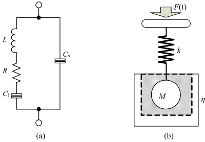
Electrical characteristics in thickness mode of PZT [3] tested in this study were comparable to the BVD equiva- lent circuit, which consists of R1 connected serially to C1
and L1 then all parallelly connected to Co [1,2,11] as
shown in Figure 1(a). The resistance, the capacitance, and the inductance were comparable to the force friction (η), spring constant (k), and mass, respectively as shown in Figure 1(b).
Assuming R1, C1, L1, and Co were constants and inde-
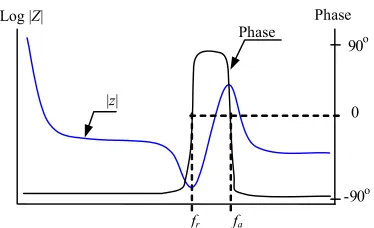
pendent on frequency and impedance [5] as given in Equation (1), the impedance equation at PZT resonance frequency (Zr), fr and fa, in terms of BVD relating pa- rameters was obtained. In Figure 2, the impedance re- sponding to fr and fa of PZT is shown.
Co L
R
C1
F (t)
k
F(t)
k
M
M η
[image:1.595.325.525.562.701.2](a) (b)
fr fa
Log |Z|
Phas
|z|
Phase e
90o
0
[image:2.595.79.266.84.198.2]-90o
Figure 2. Frequency response characteristic of piezoelectric ceramic.
(
)
(
)
1 1
0 1
R j L
Z
jωω R
+ − = + + 1 1 1 1 1 1 C
j L C
ω ω ω − ω
(1)
The calculation of BVD circuit using impedance method by the capacitor ratio (r) is as shown in Equation (2), where ωa is the angular velocity of the anti-reso- nance frequency (2πfa) and ωris the angular velocity of the resonance frequency (2πfr).
2 2 1 2 a r o r C C ω ω ω − = =
r (2)
The reactance values of C1 and L1 in BVD circuit at
low frequency range was observed. It was noted that the reactance of PZT was performed as a capacitor as shown in Equation (3).
1 1
j ωC jωω (3) Therefore,
(
R1+ jωω1− j ωC1) (
≈ R−j ωC1)
(4)Then the impedance equation of PZT can be revised as shown in Equation (5).
1 1
2 2
0 2 2
a r
R j C
jR R ω ω − + r Z ω ω ω ω = − − (5)
C1 can be calculated as given in Equation (6) by
choosing the impedance measured at low frequency range where ω is the angular velocity of the selected fre- quency and R is |Z| measured at resonance frequency.
1 r a r C 2 2 2 2 2 2 2 1 Z R − ω ω ω ω ω = − − (6)
2.2. Measurement of Dielectric Constant (K)
Measurement of K or relative permittivity (εr) of PZT is to test for the electrical characteristics which can be cal-
culated by using Equation (7), where Cf is the capaci- tance at 1 kHz, t is the thickness of PZT measured from both metal poles, A is the area of metal pole, and εo is the dielectric constant of vacuum. The dielectric constant can be varied depending on the temperature (T) of sub- stance based on Curie-Weiss Law [12] where Tc is the temperature of PZT with zero polarization, and C is Cu- rie constant (103 to 105) as given in Equation (8).
f r o C t K A ε ε
= = (7)
1 c C K T T − =
− (8)
Equations (7) and (8) can also be revised as shown in Equation (9). 1 r c C T T
ε = + (9)
−
2.3. Measurement of PZT Constant (d33)
The value of d33, measured by Piezo-D meter model
CADT (Channel Products Inc.), implies the ability to emit the electric charge of PZT when it is stimulated by mechanical force. Number 33 represents the three per- pendicular directions of compression force on PZT.
2.4. Measurement of Electromechanical Coupling Coefficient (kt)
Electromechanical coupling coefficient (kt) represents the efficiency of transformation from electrical energy to mechanical force. In Equation (10), Δf is the difference between frand fa.
2 π tan π
2 2 r t a a f f K f f
Δ
=
(
)
(10)
2.5. Measurement of Mechanical Quality Factor (Qm)
Qm represents the maximum ability of mechanical vi- bration in frrange where R1 is the impedance at resonance
frequency as given in Equation (11).
2 2 2 1 2π a m
r f a r
f Q
f R C f f
=
− (11)
3. Analysis of BVD Equivalent Circuit
(a)
N01 N02
N04 4 cm
Silver Electrod
N03
O01 e
(Thickness = 0.3 cm), (Diameter = 4 cm)
(b)
Figure 3. Physical of PZT sample: (a) Dimension of PZT; (b) Top view.
shown in Figure 4. The HP Vee program is applied to control the impedance analyzer model HP4192A via HP-IB interface and collect the impedance at 100 Hz to 1.3 MHz [4]. Then, the resonance frequency and the im- pedance at resonance frequency and lower resonance frequency will be applied to calculate R, L, and Co. The calculated value will be evaluated and compared with the value calculated by using Equation (1). In this paper, only the fundamental resonance is considered regardless the resonance frequency at harmonic period.
From experiment and measurement of PZT impedance, the calculated parameters from BVD model are as shown in Table 1. Figures 5 and 6 are illustrated the compari- son of size (|Z|m) and phase of the impedance at 100 Hz to 100 kHz measured by impedance analyzer model HP4192A and the calculated impedance (|Z|cal and Phase Cal). The impedance at 1 kHz is selected to calcu- late in Equation (6). To obtain the appropriate value of C, the impedance at lower resonance frequency is suggested such as 100 Hz, 1 kHz, 2 kHz, 3 kHz, 6 kHz, and 14 kHz. The BVD parameters are as shown in Table 2 and the percentage of error is shown in Figure 7.
4. Experiment of PZT under Temperature
Control
Physical characteristics of PZT were experimented by considering ρ, PZT constant (d33), kt, and Qm of electrical
charge at 1 kHz. In this study, only the results from N01 and N04 (details are given in Table 3) were compared under room and controlled temperatures. Figure 8 shows
HP-IB Impedance analyzer
Model : HP4192A
Piezoelectric ceramics
Personal computer
Figure 4. Impedance of PZT measurement diagram.
Figure 5. Gain impedance of PZT measurement at various frequency.
Figure 6. Phase impedance of PZT at various frequency.
the PZT experimental system connected with impedance analysis model HP4192A under temperature conditions.
Table 1. The PZT properties.
PZT properties
Fundamental resonance frequency (fr) 60.329 kHz
Fundamental anti-resonance frequency (fa) 68.971 kHz
Impedance at fr 2.847 Ω
Impedance at 1 kHz 41.040 kΩ
Impedance at 2 kHz 20.540 kΩ Impedance at 3 kHz 11.245 kΩ
Impedance at 6 kHz 6.526 kΩ
[image:4.595.71.283.99.266.2]Impedance at 14 kHz 2.863 kΩ
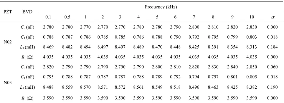
Table 2. Calculated parameters of BVD circuit at 100 Hz, 1 kHz, 2 kHz, 3 kHz, 6 kHz, and 14 kHz.
Frequency Parameters
100 Hz 1 kHz 2 kHz 3 kHz 6 kHz 14 kHz
R1 (Ω) 2.847 2.847 2.847 2.847 2.847 2.847 Co(nF) 2.9715 2.9693 2.9697 3.019 3.037 3.172
[image:4.595.313.533.291.422.2]C1 (pF) 91.22 91.16 91.17 92.69 91.33 97.39 L1 (mH) 7.63 7.64 7.64 7.51 7.47 7.15
Table 3. Physical and electrical characteristics of PZT (N01 and N04).
PZT Density d33 (10−12 C/N) Cf (nF) K (F/m) kt Qm
N01 7.38 275 4.7888 1040 0.48 846 N04 7.40 271 3.6474 1016 0.51 844
-5 0 5 10
0 20 40 60
Frequency %error
80 100
100 Hz 1 kHz 2 kHz 3 kHz 6 kHz 14 kHz
Heating elements
Figure 7. Error percentage of calculated impedance at vari- ous frequency.
HP
-I
B
Impedance analyzer
Model : HP4192A
Piezoelectric ceramics
PC
HP-IB
[image:4.595.58.285.307.418.2]Thermocouple Temperature controller Vacuum chamber
[image:4.595.59.285.455.705.2]Figure 8. PZT experimental system and impedance analysis model HP4192A.
Figure 9. Impedance and phase at the frequency ranging from 100 Hz to 80 kHz of N01.
Figure 10. Impedance and phase at the frequency ranging from 100 Hz to 80 kHz of N04.
of N01 and N04 repeatedly measured 5 times by imped- ance analysis model HP4192A under room temperature at the frequency of 1 kHz to 80 kHz.
[image:4.595.312.538.465.598.2]PZT
60.0 61.0 62.0 63.0 64.0 65.0 66.0 67.0 68.0 69.0
0 50 100 150 200 250
fr
(kH
z)
[image:5.595.72.269.85.233.2]Temperature (oC)
Figure 11. Position of PZT in temperature controlling cham- ber.
interval of measurement and the frequency was varied from 2 kHz to 80 kHz. Uncertainty of measurement and PZT was estimated by repeating 3 times of measurement.
4.1. Experimental Results under Temperature Conditions
The impedance of PZT in temperature controlled cham- ber (only N01) under specific temperature was similar to that under room temperature. However, it was observed that fr and fa were drifted. At 230˚C, fr increased about
≈1.6 kHz while fa decreased about ≈1 kHz. Therefore, the difference between frand fadecreased about 2.6 kHz as shown in Figure 12. Moreover, when the temperature was increasing, the impedance at frwas also increasing up until 190˚C and then starting to decrease as illustrated in Figure 13.
4.2. Analysis of Impedance Variation in the Range of 100 Hz to 10 kHz
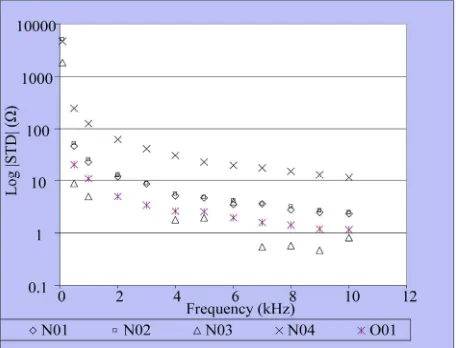
Experiment of PZT in the range of 100 Hz to 10 kHz was to calculate the impedance of BVD circuit by repeatedly measuring 30 times. An average and standard deviation of impedance are given in Figures 14 and 15, respec- tively. It can be noted that the standard deviation would increase at low frequency range and decrease as the fre- quency is rising.
4.3. Calculation of BVD Circuit Using Impedance Method
To calculate BVD circuit, average experimental values of fr, fa, and Zr at selected frequency ranging from 0.1 kHz to 10 kHz were used and then BVD parameters were obtained. The results were ranged as follows: L1≈ 0.16
mH to 0.2 mH, C1≈ 0.018 nF to 0.040 nF, Co ≈ 0.06 nF
to 0.18 nF. However, R1 was uniform due to the identical
[image:5.595.313.534.87.230.2]impedance at fr as shown in Table 4.
Figure 12. fr of PZT at various temperatures.
0.0 2.0 4.0 6.0 8.0 10.0 12.0 14.0
0 50 100 150 200 250
Zr
(
Ω
)
Temperature (oC)
Figure 13. Impedance of PZT at fr at various temperatures.
1.E+03 1.E+04 1.E+05 1.E+06
0 2 4 6 8 10 12
??????? (kHz)
log |Z
| (
ohm
)
N01 N02 N03 N04 O01
Lo
g |
Z
|(
)
Lo
g|
Z|
(Ω
)
Frequency (kHz)
Figure 14. Average values at 100 Hz to 10 kHz of N01, N02, N03, N04, and O01.
4.4. Influences of Temperature Variation on BVD Parameters
When PZT was placed in the temperature controlling chamber at 23˚C, C1 would be decrease by 72% or
0.726%/˚C that leads to 255% of increase in L1. There-
[image:5.595.315.532.265.398.2] [image:5.595.310.538.433.614.2]Table 4. BVD calculating parameters of N01 and N04 using impedance method.
Frequency (kHz) PZT BVD
0.1 0.5 1 2 3 4 5 6 7 8 9 10 σ
Co (nF) 3.870 3.850 3.850 3.840 3.840 3.850 3.860 3.870 3.880 3.890 3.910 3.930 0.090
C1 (nF) 0.947 0.941 0.940 0.940 0.940 0.941 0.943 0.946 0.948 0.952 0.956 0.961 0.021 L1 (mH) 7.146 7.190 7.199 7.203 7.202 7.192 7.179 7.159 7.142 7.112 7.079 7.044 0.159
N01
R1 (Ω) 3.331 3.331 3.331 3.331 3.331 3.331 3.331 3.331 3.331 3.331 3.331 3.331 0.000 Co (nF) 2.840 2.840 2.840 2.840 2.840 2.840 2.850 2.850 2.860 2.870 2.890 2.900 0.060
C1 (nF) 0.804 0.806 0.805 0.804 0.805 0.806 0.808 0.809 0.811 0.814 0.818 0.822 0.018 L1 (mH) 8.449 8.429 8.439 8.441 8.439 8.429 8.403 8.396 8.373 8.337 8.298 8.258 0.191
N04
R1 (Ω) 3.828 3.828 3.828 3.828 3.828 3.828 3.828 3.828 3.828 3.828 3.828 3.828 0.000
[image:6.595.59.540.100.302.2]where σ is the standard deviation.
Table 5. Percentage of BVD parameter changes as PZT temperature increasing by 230˚C.
Parameter of BVD % Difference % Difference/˚C
R1 167.0 0.726
C1 −72.0 −0.313
L1 255.0 1.109
[image:6.595.59.287.329.503.2]Co 18.1 0.079
Table 6. Physical and electrical characteristics of PZT (N02 and N03).
PZT Density d33 (10−12 C/N) Cf(nF) K (F/m) kt Qm
N02 7.42 256 3.5619 996 0.51 822 N03 7.40 262 3.5812 1002 0.51 919 Figure 15. Standard deviation values at 100 Hz to 10 kHz of
N01, N02, N03, N04, and O01.
5.1. Experiment of PZT at fr
acteristics of PZT as provided in Table 5.
Standard weights (0.5 lbs, 1.0 lbs, and 1.5 lbs) were pressed to estimate fr, fa, and Zr as shown in Table 7
compared to weightless condition. The comparison was shown in Table 8. It can be noted that PZT pressed by 1.5 lbs standard weight would express higher fr and fa by
≈0.24 kHz and 2 kHz, respectively. However, Zr would be varied by the weight pressing and become stable at
≈6.5 Ω.
5. Experiment of PZT under
Mechanical Force
The parameters which was use in consideration of phy- sical and electrical characteristics of PZT consists of ρ,
d33, kt, and Qm at 1 kHz. In this case, comparison of N02
and N03 is as shown in Table 6.
Measurement of Zr under mechanical force was per- formed by using 0.5 lbs, 1.0 lbs, and 1.5 lbs of brass standard weights at room temperature. Each measure- ment was varied the frequency starting from 2 kHz to 80 kHz and repeated 30 times for calculating an average value. Figures 16(a) and (b) illustrate the experimental system and the brass standard weights, respectively.
5.2. Experiment of Zr of PZT Connected Serially
with Specific Capacitors
[image:6.595.308.536.354.440.2]HP- IB Impedance analyzer
Model : HP4192A
Piezoelectric ceramics PC
Standard weight
(a)
[image:7.595.61.283.85.395.2](b)
[image:7.595.315.531.236.363.2]Figure 16. Impedance measurement using Impedance ana- lysis model HP4192A and standard weight pressing: (a) System diagram; (b) Brass standard weights.
Table 7. fr, fa, and Zrof PZT under mechanical force loads.
Under force load (lb) PZT Parameter
0 0.5 1 1.5
Zr 3.601 8.770 7.536 10.553
fr 61.550 61.850 61.700 61.850
N02
fa 69.800 69.650 69.950 79.099
Zr 3.964 5.575 10.587 5.506
fr 61.250 61.400 61.400 61.400
N03
fa 69.350 69.500 69.350 69.350
Table 8. Variation of fr, fa, and Zrof PZT under mechanical
force loads.
Under force load (lb) Parameter
0.5 1 1.5
ΔZr 2.602 5.380 6.560
Δfr 0.180 0.180 0.240
Δfa 0.210 0.300 2.130
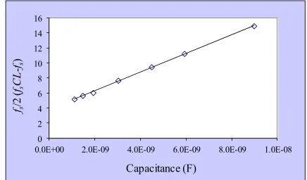
measured. The relationships of fs/2 (fsCL-fs) are as illus- trated in Figures 17-20 where fs is the serial resonance frequency based on IEEE method [4,5]. The slope of linear relationship is 1/C1 as shown in Table 9.
5.3. Calculation of BVD Using Impedance Method
[image:7.595.313.531.407.535.2]The average values of fr, fa, and Zr at resonance fre- quency obtained from experiments of N02 and N03 were used for analyzing BVD. By selecting the frequency ranging from 0.1 kHz to 10 kHz, it can be observed that
Figure 17. fr, fa, and Zr of N02 connected serially with vari-
ous capacitors.
0 2 4 6 8 10 12 14 16
0.0E+00 2.0E-09 4.0E-09 6.0E-09 8.0E-09 1.0E-08
fs
/2
(
fs
CL
-fs
)
Capacitance (F)
Figure 18. fs/2(fsCL-fs) of N02 connected serially with various
capacitors.
Figure 19. fr, fa, and Zr of N03 connected serially with vari-
[image:7.595.59.286.462.610.2] [image:7.595.312.532.573.707.2] [image:7.595.58.283.650.735.2]impedance method. The differences are given in Table 12.
0 2 4 6 8 10 12 14 16
0.0E+00 2.0E-09 4.0E-09 6.0E-09 8.0E-0
fs
/2
(
fs
CL
-fs
)
Capacitance (F)
9 1.0E-08
[image:8.595.60.286.86.219.2]6. Conclusion
Figure 20. fs/2(fsCL-fs) of N02 connected serially with various
[image:8.595.58.285.277.335.2]capacitors.
Table 9. Slopes of fs/2(fsCL-fs).
PZT Slope = 1/C1 (109) C1 (nF)
N02 1.237 0.808 N03 1.235 0.810
From calculation, it was observed that |Z| and Z(θ) of the impedance ranging from low frequency to fr and fa tended to be equal to the impedance measured by im- pedance analysis model HP4192A. Selecting low fre- quency range (100 Hz, 1 kHz, and 2 kHz) for calculating
C would cause the error of |Z| by ≈−1%, On the other hand, selecting the impedance and frequency at 3 kHz the error would be exhibit less than 1%. However, the impedance and frequency at 14 kHz would exhibit the greater error by ≈5% because ωL can much influence the impedance while 1/ωL decreases. Therefore, the im- pedance selected for calculating should have the fre- quency lower than f fa2− fr2. Considering the per- centage of impedance error, it can noted that the imped- ance at the frequency of 100 Hz, 1 kHz, and 2 kHz would provide the similar results with 20% - 25% of the maximum error of fa. From experiment of the calculated impedance, the accuracy of fr and fa was ±0.0033 kHz with the standard deviation of 0.00129 kHz which would be reliable for calculating BVD circuit. From experiment of accuracy which was compared between Zr of BVD equivalent circuit and Zr from measurement, it can be noted that Zr at fr of BVD circuit calculated by imped- ance method and IEEE 176-1987 would exhibit the error by ≈2.37% which was lower than HP4194 method (≈4%). It would be because the impedance analysis using im- pedance analysis model HP4192A is applied the pro- gram to estimate fr more accurately. However, R1 was
less different as it was a specific resistance at resonance frequency. Considering the influence of temperature on PZT characteristic, it was noted that the increase of tem- perature would contribute to less difference of fr and fa.
Co ≈ 0.06 nF, C1≈ 0.018 nF, L1≈ 0.184 mH to 0.190 mH
while R1 was identical due to the same impedance at fr as
given in Table 10.The Table 11 shows the comparison of BVD parameters calculated by using impedance me- thod, IEEE method, and HP4194 where IEEE method is the method of IEEE 176-1987, Δ1 is the percentage of
difference between values obtained from impedance and IEEE 176-1987 method, and Δ2 is the percentage of dif-
ference between values obtained from impedance and HP4194 method.
5.4. Influences of Temperature on BVD Parameters under Mechanical Force
Variation of fr, fa, and Zr when PZT was pressed by standard weights was calculated for Co, C1, and L1 by
Table 10. Calculation of BVD parameters based on impedance method: a case of N02 and N03.
Frequency (kHz) PZT BVD
0.1 0.5 1 2 3 4 5 6 7 8 9 10 σ
Co (nF) 2.780 2.780 2.770 2.770 2.770 2.780 2.780 2.790 2.800 2.810 2.820 2.830 0.060
C1 (nF) 0.788 0.787 0.786 0.785 0.785 0.786 0.788 0.790 0.792 0.795 0.799 0.803 0.018 L1 (mH) 8.469 8.482 8.494 8.497 8.497 8.489 8.470 8.448 8.425 8.391 8.354 8.313 0.184
N02
R1 (Ω) 4.035 4.035 4.035 4.035 4.035 4.035 4.035 4.035 4.035 4.035 4.035 4.035 0.000 Co (nF) 2.820 2.790 2.790 2.790 2.790 2.790 2.800 2.810 2.820 2.830 2.840 2.850 0.060
C1 (nF) 0.795 0.788 0.787 0.787 0.787 0.788 0.789 0.792 0.794 0.797 0.801 0.805 0.018 L1 (mH) 8.488 8.559 8.570 8.571 8.572 8.561 8.549 8.518 8.496 8.463 8.425 8.382 0.190
N03
R1 (Ω) 3.590 3.590 3.590 3.590 3.590 3.590 3.590 3.590 3.590 3.590 3.590 3.590 0.000
[image:8.595.58.540.557.733.2]Table 11. Comparison of average BVD parameters from each method.
PZT BVD
Impedance method
(1 kHz) IEEE HP4194 Δ1 Δ2
Co (nF) 2.770 2.852 2.707 2.96% 2.27%
C1 (nF) 0.786 0.808 0.791 2.80% 0.64% L1 (mH) 8.494 8.258 8.483 2.78% 0.13%
N02
R1 (Ω) 4.035 4.035 3.415 0.00% 15.37% Co (nF) 2.790 2.872 2.719 2.94% 2.54%
C1 (nF) 0.787 0.810 0.791 2.92% 0.51% L1 (mH) 8.570 8.328 8.572 2.82% 0.02%
N03
R1 (Ω) 3.590 3.590 4.056 0.00% 12.98%
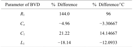
Table 12. Percentage of BVD parameter variation with 1.5 lbs standard weight pressing.
Parameter of BVD % Difference % Difference/˚C
R1 144.0 96
Co −4.96 −3.30667
C1 21.22 14.14667
L1 −18.14 −12.0933
However, the increase of Zr would cause the variation of BVD calculated parameters such as decrease of C1, in-
crease of R1, L1, and Co. On the other hand, the influ-
ences of mechanical force load on PZT parameters would cause fr, fa, and Zr increase that also contribute to R1 and
C1 increase while L1 and Codecrease.
REFERENCES
[1] S. Sherrit, H. D. Wiederick and B. K. Mukherjee, “Accu- rate Equivalent Circuits for Unloaded Piezoelectric Re- sonators,” IEEE Ultrasonics Symposium Proceedings, Vol. 2, 1997, pp. 931-935.
[2] S. Sherrit, H. D. Wiederick, B. K. Mukherjee and M. Sayer, “An Accurate Equivalent Circuits for the Unloaded Pie-
zoelectric Vibrator in the Thickness Mode,” Journal of Physics D: Applied Physics, Vol. 30, No. 16, 1997, pp. 2354-2363. doi:10.1088/0022-3727/30/16/014
[3] C. Jeerapan, W. Sriratana, P. Julsereewong and S. Kum- mool, “Analysis of Appropriate Parameters for Piezoelec- tric Ceramic Utilization by Using BVD Model,” ICCAS 2005, International Conference on Control, Automation and System, Gyeonggi-Do, 2-5 June 2005, pp. 2067-2070. [4] “An American National Standard IEEE Standard on Pie-
zoelectricity,” IEEE Ultrasonics, Ferroelectrics, and Fre- quency Control Society, New York, 1988, ANSI/IEEE Std 176-1987.
[5] “Standard Definitions and Method of Measurement for Piezoelectric Vibrators,” The Institute of Electrical and Electronics Engineers Inc., New York, 1966, IEEE No. 177.
[6] J. G. Smits, “Iterative Method for Accurate Determination of Real and Imaginary Parts of the Materials Coefficients of Piezoelectric Ceramics,” IEEE Transactions on Sonics and Ultrasonics, Vol. 23, No. 6, 1976, pp. 393-402. doi:10.1109/T-SU.1976.30898
[7] S. Sherrit, H. D. Wiederick and B. K. Mukherjee, “Non- Iterative Evaluation of the Real and Imaginary Material Constants of Piezoelectric Resonators,” Ferroelectrics, Vol. 134, No. 1-4, 1992, pp. 111-119.
doi:10.1080/00150199208015574
[8] Q. C. Xu, A. R. Ramachandran and R. E. Newnham, “Re- sonance Measuring Technique for Complex Coefficients of Piezoelectric Composites,” Journal of Wave-Material Interaction, Vol. 2, 1987, pp. 105-122.
[9] B. Jaffe, W. R. Cook Jr and H. Jaffe, “Piezoelectric Ce- ramics,” Journal of Sound and Vibration, Vol. 20, No. 4, 1972, pp. 562-563.
[10] T. Ikeda, “Fundamentals of Piezoelectricity,” 19th Edi- tion, Oxford University Press, New York, 1990.
[11] S. Fujishima, K. Togawa and S. Ohta, “Analysis and De- sign of the Piezoelectric Ceramic Resonator Osillators,” 41st Annual Symposium on Frequency Control, Pennsyl- vania, 27-29 May 1987, pp. 391-397.
doi:10.1109/FREQ.1987.201052
[image:9.595.57.287.311.393.2]