A Low Power Single-stage LED Driver Operating between
Discontinuous Conduction Mode and Critical Conduction
Mode
AL-NAEMI, Faris, YANG, Jianbo and ZHANG, Weiping
Available from Sheffield Hallam University Research Archive (SHURA) at:
http://shura.shu.ac.uk/13078/
This document is the author deposited version. You are advised to consult the
publisher's version if you wish to cite from it.
Published version
AL-NAEMI, Faris, YANG, Jianbo and ZHANG, Weiping (2015). A Low Power
Single-stage LED Driver Operating between Discontinuous Conduction Mode and Critical
Conduction Mode. Energy Procedia, 74, 817-825.
Copyright and re-use policy
See
http://shura.shu.ac.uk/information.html
Energy Procedia 74 ( 2015 ) 817 – 825
ScienceDirect
1876-6102 © 2015 Published by Elsevier Ltd. This is an open access article under the CC BY-NC-ND license (http://creativecommons.org/licenses/by-nc-nd/4 .0/).
Peer-review under responsibility of the Euro-Mediterranean Institute for Sustainable Development (EUMISD) doi: 10.1016/j.egypro.2015.07.817
International Conference on Technologies and Materials for Renewable Energy, Environment and
Sustainability, TMREES15
A Low Power Single-Stage LED Driver
Operating between
Discontinuous Conduction Mode and Critical Conduction Mode
Faris Al-Naemi
a, Jianbo Yang
a, Weiping Zhang
baSheffield Hallam University, 153Arundel St,Sheffield, S1 2NU, United Kingdom bNorth China University of Technology, 5Jianyuanzhuang St, Beijing, 100144,China
Abstract
A novel single-stage single-switch (S4) LED driver is proposed in this paper. The paper focuses on the operation principles of the
power stage circuit with an operation switched between Critical Conduction Mode (CRM) and Discontinuous Conduction Mode (DCM), including steady state analysis, simulation and backed up by experimental results. The results verify that this proposed LED driver can obtain a high power factor (PF) and the dc output is relatively stable.
© 2015 The Authors. Published by Elsevier Ltd.
Peer-review under responsibility of the Euro-Mediterranean Institute for Sustainable Development (EUMISD).
Keywords:CRM; DCM; PFC; Single-stage
1.Introduction
Light-Emitting-Diode (LED) has become a commonly used solid-state light source in general lighting applications [1, 2]. It has longer lifetime and has no poison mercury content compared with the conventional
fluorescent lamp [3]. So LEDs now have been drawing attention as a state-of-the-art illuminator and the driver of LEDs in the markets also keeps up with the progress in this promising field [4]. The active PFC converters can be
implemented using either the “two-stage” approach or the “single-stage” approach. The most commonly used approach in ac/dc conversion that meets high power quality requirements is the “two-stage” approach [5]. The “two
-stage” approach includes two power-conversion processes. The first stage is a PFC (power factor correction) stage like a boost converter, and the second stage normally is a dc/dc converter to regulate the output voltage. This approach has good performances for power factor (PF) and output-voltage regulation. The main disadvantage is the high cost due to an increase in the device count. This “two-stage” PFC ac/dc converter usually increases the cost by about15%, compared with that of an ac/dc converter without PFC [6-9].
© 2015 Published by Elsevier Ltd. This is an open access article under the CC BY-NC-ND license (http://creativecommons.org/licenses/by-nc-nd/4.0/).
818 Faris Al-Naemi et al. / Energy Procedia 74 ( 2015 ) 817 – 825
In order to reduce the cost, the single-stage approach, which integrates the PFC stage with a dc/dc converter into one stage, has been presented in this paper. These integrated single-stage PFC converters usually use a boost converter to achieve PFC in discontinuous conduction mode (DCM) operation and constant on-time control, which is known as the voltage-follower approach. This approach is simpler to be implemented than the multiplier approach (usually for continuous conduction mode (CCM) operation); however, it requires an input filter to obtain a good input current waveform. In this paper, the proposed converter operates between the DCM and critical conduction mode (CRM). The input current falls to zero without dwelling at zero in part of the half-line frequency cycle. Therefore, for a given throughput power, the proposed operation involves lower peak input current than the pure DCM operation and requires smaller input filter. Furthermore, the dc bus voltage is controlled directly, which solves the high voltage stress problem existed in the single-stage PFC converter.
2.Operation Principle
2.1.Power stage
The proposed single-stage PFC converter is briefly illustrated in Fig.1. Although the power stage circuit has only one switch, two conversion stages can be identified. In fact, input inductor L1, rectifier D1, D2, switch Q1 and internal energy-storage capacitor Cp form a DCM boost power stage, while switch Q1 , the transformer T1, freewheeling diode D3, output rectifier D4 and output-filter capacitor C2 make up a forward power stage. Referring to Fig.1, the operating principle of the proposed converter can be explained as follows;
When Q1 is turned on, L1 is energized by the rectified input voltage and inductor current increases. At the same time, the primary of the transformer T1 is energized by Cp. D4 is forward biased. Thus, the energy is being transferred to the output.
When Q1 is turned off, energy stored in L1 is being transferred to Cpand is decreasing to zero. D3 is forward biased and Cp is energized by the demagnetization winding of T1 to restore the transformer core. As a result, is also decreasing to zero. D4 is reverse biased and output is supplied by C2.
To achieve low harmonic distortions in , L1 is usually operated in the DCM [10]. The proposed converter operates in a mode switching between DCM and BCM. This obviously further reduces the input current distortion. The control scheme will be discussed in the following section.
Fig.1 proposed single-stage converter
2.2.CRM &DCM
Converters in critical conduction mode operation are generally accepted for low-power PFC applications. At CRM, such as Boost, a turn-on switching process is initiated when the output diode current falls to zero, while a turn-off switching process is established when the peak transistor current reaches the threshold level set by the controller output. This ensures the converter operating at the boundary of Continuous Conduction Mode (CCM) and Discontinuous Conduction Mode (DCM) at the expense of variable switching frequency over the AC line period.
AC1
AC2 POS
NEG AC
INPUT OUTPUTDC
.
.
.
.
.
.
.
.
.
B
C1 L1 iin D1 D2 Q1 Cp n1n3 n2
T1
D3
D4
Referring to Fig.2, the proposed converter operates in a different way from the conventional CRM and DCM. The turn-on switching signal is set out when the current through Cp rather than the output diode current falls to zero. This makes sure that the core returned to its initial state during every switching cycle. A turn-off switching process is also established when the peak transistor current reaches the threshold level set by the controller output.
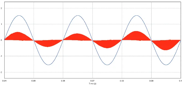
The operation principle is determined by which current falls to zero first, the current through L1 or the current through D3. If the current through L1 falls to zero firstly, Q1 will not be turned on until the current through D3 becomes zero. Therefore, the converter operates in DCM. On the contrary, when current though D3 decreases to zero first, the turning-on of Q1 is activated when the current through L1 falls to zero. Thus, the converter operates in CRM. As a result, as depicted in Fig.3, the operation of the proposed converter switches between DCM and CRM during a half-line period. In Fig.3, is the rectified input voltage and is the current through L1. It is obvious that the current through L1 stays at zero in part of the half-line cycle, while it drops to zero but without dwelling at zero in the rest, which indicates that the operation of the converter switches between DCM and CRM.
Fig.2 control of the proposed converter with L6561
Fig.3 current through L1
DCM CRM
V
ii
ini
in,average AC1 AC2 POS NEG Vin Vout.
.
.
.
.
.
.
.
.
B C1 L1 iin D1 D2 Q1 Cp n1n3 n2
820 Faris Al-Naemi et al. / Energy Procedia 74 ( 2015 ) 817 – 825
3.Steady-state analysis
As plotted in Fig.3, the input voltage is ||. The peak inductor current is enveloped by rectified sinusoid
() = || (1)
≈ 4 (2)
Pin is input power. When the transistor is conducting, the peak transistor current can be expressed as:
() =1
() || (3)
The transistor “on” time can be obtained by substituting (1) into (3).
() == (4)
This equation shows that the transistor “on” time of CRM is constant. When the discharging time of L1 is equal to the demagnetizing time of the demagnetization winding of T1, the converter comes to the boundary of the DCM and CRM.
The discharging time of L1 is:
=||
− || (5)
According to Faraday law, when Q1 is turned on, the change of the flux,∆Φ in the transformer is:
∆ =
(6)
n1 is the number of turns of the transformer primary winding. When Q1 turns off, the core of T1 should be restored. Then, the demagnetizing time can be obtained as:
=
(7)
n3 the number of turns of the transformer auxiliary winding .Substituting of (4) into (7), the demagnetization time tdm is:
=
(8)
When = , the converter is in the boundary of DCM and CRM. When > , the converter operates in DCM. When < , the converter operates in CRM.
=
||
− || (9)
Further simplification yield:
=
||
− || (10)
According to the discussion above, the working conditions of the converter are: DCM:
<
||− 1 (11)
CRM:
>
||− 1 (12)
As shown in (11) and (12), the proposed converter will operate in DCM when:
|| <
1 +
(13)
And it will operate in CRM when:
|| >
1 +
(14)
This conclusion is in accordance with the waveforms shown in Fig.3. When the rectified input voltage is in the vicinity of zero, the converter is in DCM. When the input rectified voltage rises from 0 to its peak value the converter enters into the CRM operation mode.
4.Simulation and experiments
[image:6.544.118.435.482.631.2]The proposed scheme has been tested with simulation and experiment. The simulation was carried out by Psim9.0 and was designed to have a 220v input and 40V/1A output. The results of a closed loop simulation are illustrated in Fig. 4 to 7.
822 Faris Al-Naemi et al. / Energy Procedia 74 ( 2015 ) 817 – 825
Fig. 5 output voltage 40v (Ripple: 3v)
The simulation is implemented in a single closed loop control. The compensation is a capacitor. The power stage circuit is imitated to be controlled by L6561 which is usually used for the CRM PFC applications.
Fig. 4 shows that the input current is sinusoidal and is in phase with the input voltage. This proves that the proposed converter can have a high power factor switching between the CRM and DCM operation modes.
Fig. 6 input inductor (L1 in Fig.1) CRM
Fig. 7 input inductor (L1 in Fig.1) DCM
0.1 0.12 0.14 0.16 0.18 0.2
Time (s) 20
30 40 50 60VP1
0.16498 0.164985 0.16499 0.164995 0.165 0.165005
Time (s) 0
0.2 0.4
I(L1)
0.139816 0.139818 0.13982 0.139822 0.139824 0.139826
Time (s) 0
0.01 0.02 0.03
[image:7.544.124.417.320.615.2]The output voltage is shown in Fig.5. The output voltage is a stable dc output. Fig.6 and Fig.7 depict the details of the input inductor (L1 in Fig.1) current. They prove that the converter operate differently. During partial of the operation, the inductor L1 current falls to zero and the converter operates in DCM. In the other part of the operation, the inductor current (L1) falls to zero without dwelling at zero. This shows that the converter operates in CRM. This is the same as waveforms in Fig.3.
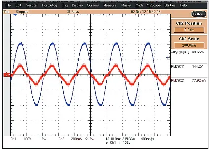
A laboratory prototype for the proposed converter at 8W output was built to verify the control strategy and evaluate the circuit performance while the output voltage is kept to 23V. The circuit diagram is given in Fig. 2. The MOSFET IRFPESO, diode MUR480 and PFC Controller L6561 are used in the prototype. The inductors (L1=1mH) and transformer (T1) are realized in an EFD core. Experimental waveforms are shown in Fig. 8 to 10.
Fig. 8 shows that the input current is well regulated and is in phase with the input voltage. The output voltage shown in Fig.9 is stabilized at 23V with a ripple of 1V. The efficiency is almost 82%. Fig. 10 proves that the all the harmonics of the input current can meet the IEC61000-3-2 requirements for class C. The power factor is 0.98
[image:8.544.63.487.216.518.2].
Fig. 8 input voltage (140Vac) and input current (77mA rms)
5.Conclusion
824 Faris Al-Naemi et al. / Energy Procedia 74 ( 2015 ) 817 – 825
Fig. 9 output voltage (23v) ripple 1v
[image:9.544.82.476.359.630.2]References
[1] Maxim-Dallas Semiconductor, “Why drive white LEDs with constant current,” Jun. 2004
[2] C. Y. Wu, T. F. Wu, J. R. Tsai, Y. M. Chen, and C. C. Chen, “Multistring LED backlight driving system for LCD panels with colour sequential display and area control,” IEEE Trans. Ind. Electron., vol. 55, no. 10, pp. 3791–3800, 2008
[3] S. K. Kim, H. S. Han, Y. J.Woo, and G. H. Cho, “Detection and regulation of CCFL current and open-lamp voltage while keeping floating
condition of the lamp,” IEEE Trans. Ind. Electron., vol. 53, no. 2, pp. 707–709, 2006
[4] Xunwei Zhou, Mauro Donati, Luca Amoroso, and Fred C. Lee, “Improved Light-Load Efficiency for Synchronous Rectifier Voltage
Regulator Module,” IEEE Transactions on Power Electronics, vol. 15, no. 5, pp. 826-834, 2000
[5] El Aroudi A., Haroun R., Cid-Pastor A., Martinez-Salamero L.: 'Suppression of Line Frequency Instabilities in PFC AC-DC Power Supplies by Feedback Notch Filtering the Pre-Regulator Output Voltage', IEEE Trans. Circuit and systems I, vol.60, no.3, pp. 796-809, 2013 [6] J. Qian, Q. Zhao and F. C. Lee, “Single stage single-switch power factor correction AC/DC converters with DC-bus voltage feedback for
universal line applications,” IEEE Trans. on Power Electronics, vol.13, no.6, pp. 1079–1088, 1998
[7] Pritam Das., Majid Pahlevaninezhad., Gerry Moschopoulos.: 'Analysis and Design of a New AC–DC Single-Stage Full-Bridge PWM Converter With Two Controllers'. IEEE Trans. Ind. Electron., vol.60, no.11, pp. 4930-4946, 2013
[8]M. Arias., D. G. Lamar., J. Sebastian., D. Balocco., A. A. Diallo.: 'High efficiency LED driver without electrolytic capacitor for street lighting', IEEE Trans. Ind. Appl., vol. 49, no.1, pp. 127–137, 2013
[9] Hugo Santos Ribeiro., Beatriz Vieira Borges, “Solving Technical Problems on the Full-Bridge Single-Stage PFCs,” IEEE Trans. Ind. Electron., vol.61, no.5, pp.2264-2277, 2014
[10]M. Madigan, R. Erickson, E. Ismail, “Integrated high-quality rectifier-regulators,” IEEE Power Electronics Specialists Conf. (PESC)