methodology for CPU and GPU architectures
KELEFOURAS, Vasileios <http://orcid.org/0000-0001-9591-913X>,
KRITIKAKOU, Angeliki, MPORAS, Iosif and VASILEIOS, Kolonias
Available from Sheffield Hallam University Research Archive (SHURA) at:
http://shura.shu.ac.uk/18333/
This document is the author deposited version. You are advised to consult the
publisher's version if you wish to cite from it.
Published version
KELEFOURAS, Vasileios, KRITIKAKOU, Angeliki, MPORAS, Iosif and VASILEIOS,
Kolonias (2016). A high-performance matrix-matrix multiplication methodology for
CPU and GPU architectures. Journal of Supercomputing, 72 (3), 804-844.
Copyright and re-use policy
See
http://shura.shu.ac.uk/information.html
(will be inserted by the editor)
A high performance Matrix-Matrix Multiplication
Methodology for CPU and GPU architectures
Vasilios Kelefouras, Angeliki Kritikakou, Iosif Mporas, Vasilios Kolonias
the date of receipt and acceptance should be inserted later
Abstract Current compilers cannot generate code that can compete with
hand-tuned code in efficiency, even for a simple kernel like Matrix-Matrix Multiplication. A key step in program optimization is the estimation of optimal values for parameters such as tile sizes and number of levels of tiling. The scheduling parameter values selection is a very difficult and time-consuming task since parameter values depend on each other; this is why they are found by using searching methods and empirical techniques. To overcome this problem, the scheduling sub-problems must be optimized together, as one problem and not separately.
In this paper a Matrix-Matrix Multiplication methodology is presented where the optimum scheduling parameters are found by decreasing the search space theoretically while the major scheduling sub-problems are addressed to-gether as one problem and not separately according to the hardware architec-ture parameters and input size; for different hardware architecarchitec-ture parameters and/or input sizes, a different implementation is produced. This is achieved by fully exploiting the software characteristics (e.g., data reuse) and hardware ar-chitecture parameters (e.g., data caches sizes and associativities), giving high quality solutions and a smaller search space. This methodology refers to a wide range of CPU and GPU architectures.
Keywords Matrix-Matrix Multiplication, Data reuse, optimization, SIMD,
memory hierarchy, loop tiling
1 Introduction
Matrix-Matrix Multiplication (MMM) is an important kernel in most varied domains and application areas. Its performance is of great practical importance and it highly depends on memory management; the most performance critical
sub-problems are these of finding the schedules with the minimum numbers of i) L1 data cache accesses, ii) L2 data cache accesses, iii) L3 data cache accesses, iv) main memory data accesses, v) addressing instructions. The above sub-problems depend on each other (e.g., a decrease on the number of L2 data cache accesses will consequently increase the number of L1 data cache accesses) and this is why they should be addresses together as one problem and not separately (in [1], a methodology for Matrix-Vector Multiplication is given).
Toward this, much research has been done, either to simultaneously opti-mize only two phases, e.g., register allocation and instruction scheduling (the problem is known to be NP-complete) [2] [3] or to apply predictive heuristics [4] [5]. Nowadays compilers and related works, apply either iterative compi-lation techniques [6] [7] [8] [9], or both iterative compicompi-lation and machine learning compilation techniques to restrict the configurations’ search space [10] [11] [12] [13] [14] [15]. A predictive heuristic tries to determine a priori whether or not applying a particular optimization will be beneficial, while at iterative compilation, a large number of different versions of the program are generated-executed by applying transformations and the fastest version is se-lected; iterative compilation provides good results, but requires extremely long compilation times.
The state of the art (SOA) hand/self-tuning libraries for linear algebra, such as ATLAS [16], OpenBLAS [17], Eigen [18], Intel MKL [19], PHiPAC [20] and a few of the many noteworthy papers from the past such as [21] [22] [23] [24] for CPUs and [25] [26] for GPUs, do not give a theoretical solu-tion; instead, they find the performance critical parameter values mostly by searching and by using heuristics and empirical techniques. The selection of the parameter values is a difficult and time consuming task for two reasons. First, many parameters have to be taken into account, such as the number of the levels of tiling, tile sizes, loop unroll depth, software pipelining strategies, register allocation, code generation, data reuse, loop transformations. Second, the optimum parameters for two slightly different architectures are different. Such a case is MMM algorithm, which is a major kernel in linear algebra and also the topic of this paper. In this paper the optimum scheduling parameters are found by decreasing the search space theoretically, for a wide range of CPU (including multi-cores) and GPU architectures.
line size, the number, the latencies and the type of the CPU function units, the number of the load/store units) and software characteristics (number of matrix operations, number of addressing instructions). Fourth, the proposed methodology, due to the major contribution of number three above gives a smaller search space, a smaller code size and a smaller compilation time, as it does not test a large number of alternative schedules.
The proposed methodology is compared with the state of the art software libraries of ATLAS and Intel MKL. Although a performance comparison with Intel MKL is unfair, a detailed experimental analysis has been made as it is the fastest MMM library in the world for Intel general purpose processors. A performance comparison with Intel MKL is unfair for two reasons. First, Intel MKL developers have access to all the Intel processor architecture de-tails which we do not, e.g., victim cache, hardware prefetchers; this is why Intel MKL library is the fastest library on Intel processors only. Second, In-tel MKL loop kernels are written in assembly code while our method in C (assembly code is always more efficient); Intel developers write assembly code to deal with the low level transformations, e.g., register allocation, instruc-tion selecinstruc-tion and instrucinstruc-tion scheduling. The proposed methodology lies at a higher level of abstraction and it is used to wide range of computer architec-tures. Implementing the proposed methodology in assembly code is beyond the scope of this paper and thus the low level transformations are applied by the target compiler (which is less efficient). The scope of this paper is not to pro-vide the peak-performance MMM implementations, but to analytical give the architecture dependent high level transformation parameters (e.g., tile sizes) that achieve peak-performance. We strongly believe that if could modify the MKL library scheduling parameters according to the proposed methodology, an even higher performance would be achieved.
The proposed methodology is compared to the SOA libraries of ATLAS and Intel MKL for CPUs and cuBLAS for GPUs. The evaluation is done by using Intel Xeon CPU E3-1241 v3, Pentium Intel i7-2600K, Valgrind tool [28], ARMv7-a on GEM5 simulator, PowerPC-440 on Xilinx FPGA Virtex-5, Nvidia GeForce GTX-580, Gem5 [29] and SimpleScalar simulator [30].
The remainder of this paper is organized as follows. In Sect. 2, the related work is given. The proposed methodology is presented in Sect. 3. In Sect. 4, the experimental results are presented while Sect. 5 is dedicated to conclusions.
2 Related Work
The problem of speeding up MMM is studied the last decates. A historical perspective is given in [31] [32] [33] [34] [35] [36] [37] [38] [39] [40] [41]; these works present how hardware and software can work on scalable multi-processor systems for matrix algorithms.
ways of performing a given kernel operation are supplied, and timers are used to empirically determine which implementation is best for a given architec-tural platform. ATLAS uses BLAS implementations. The BLAS (Basic Linear Algebra Subprograms) are routines that provide standard building blocks for performing basic vector and matrix operations. Intel Math Kernel Library (Intel MKL) [19] is a computing math library of highly optimized, exten-sively threaded routines for applications that require maximum performance. Intel MKL library has been written by Intel and this is why it performs the best for Intel processors only. MKL kernels have been written in assembly for maximum performance. During the installation of ATLAS and Intel MKL, on the one hand an extremely complex empirical tuning step is required, and on the other hand a large number of compiler options are used, both of which are not included in the scope of this paper. Although ATLAS is one of the SOA libraries for MMM algorithm, its techniques for supplying different implemen-tations of kernel operations concerning memory management are empirical and hence it does not provide any methodology for it.
Regarding MMM implementations for one core, many related works exist such as [22, 23, 21, 46–52]. In [22] BLIS is presented; BLIS is a framework for rapid instantiation of BLAS. In [23], BLIS extends the GotoBLAS approach to implement peak performance MMM implementations. In [21] a system-atic analysis of the high-level issues affecting the design of high-performance matrix multiplication is given. Reference [24] gives a significant theoretical background on finding the optimum scheduling parameters, but it refers to specific CPUs architectures only. In [51], analytical models are presented for estimating the optimum tile size values assuming only fully associative caches, which in practice are very rare. The aforementioned works refer to specific CPU architectures only and find the scheduling parameters mostly by using empirical techniques.
Although loop-tiling is necessary to achieve high performance, the above works do not find the tile sizes and the number of levels of tiling, by taking into account the cache sizes, their associativities and the data arrays layouts, together as one problem; instead searching is applied. Let us give an example. According to ATLAS [16] (only cache size is taken into account), the size of three rectangular tiles (one for each matrix) must be smaller or equal to cache size; however, the elements of these tiles are not written in consecutive main memory locations and thus they do not use consecutive data cache locations; this means that having a set-associative cache, they cannot simultaneously fit in data cache due to the cache modulo effect. Moreover, even if the tiles elements are written in consecutive main memory locations (different data array layout), the three tiles cannot simultaneously fit in data cache if the cache is two-way associative or direct mapped. We will show that loop tiling is efficient only when cache size, cache associativity and data array layouts, are addressed together as one problem and not separately.
going to be parallelized. The vast majority of previous works regarding multi-core architectures, deal with cluster architectures; they partition the MMM problem into many distributed memory computers (distributed memory refers to a multiple-processor computer system in which each processor has its own private memory). SRUMMA [64] describes one of the best parallel algorithm which is suitable for clusters and scalable shared memory systems. Although SRUMMA minimizes the communication contention between CPUs, it does not optimize the MMM problem for one CPU (it runs thecblas sgemm AT-LAS optimized routine). Furthermore, about half of the above works, use the Strassen’s algorithm [65] to partition the MMM problem into many multi-core processors; Strassen’s algorithm minimizes the number of the multiplication instructions sacrificing the number of add instructions and data locality. The MMM code for one core, is either given by Cilk tool [66] or bycblas sgemm routine of ATLAS. At last, [67] and [68] show how shared caches can be utilized. All the above works, are empirical techniques and do not provide a theoretical model.
Regarding GPUs, several related works exist such as [25] [26] [69] [70] [71] [72] [73] [74] [75] [76]. Reference [26] show how to modify the MAGMA GEMM kernels in order to use more efficient the Fermi architecture. [69] presents a method for producing MMM kernels tuned only for a specific archi-tecture, through a canonical process of heuristic autotuning, based on gener-ation of multiple code variants and selecting the fastest ones through bench-marking. [71] provide implementations of Strassen’s MMM algorithm as well as of Winograd’s variant; they show that only for square matrices of very large sizes (16384×16384) achieve 33% speedup overcblas sgemm(ATLAS routine for data of type float) and 21% overcblas dgemm(ATLAS routine for data of type double). [73] presents an in-depth study to reveal interesting trade-offs between shared memory and the hardware-managed L1 data caches for MMM. [74] investigates different performance techniques such as tiling, memory coa-lescing, prefetching, and loop unrolling, in trying to evaluate which method is the most efficient. [75] provides theoretical analysis why performance draw-backs appear for specific problem sizes when using cache memories. Finally, in [76], different data arrays layouts are evaluated, such Z-Morton and X-Morton. All the above works, are empirical techniques and do not give a methodology. In contrast to the proposed methodology, the above works find tile sizes mostly by searching, since they do not exploit all the h/w and the s/w con-straints. However, if these constraints are fully exploited, the optimum solution can be found by enumerating only a small number of solutions; in this paper, tile sizes are given by inequalities which contain the cache sizes and cache associativities.
3 Proposed Methodology
for (i=0; i<N; i++) for (j=0; j<M; j++)
for (k=0; k<P; k++) C[i][j] += A[i][k] * B[k][j];
Fig. 1 MMM unoptimized code
numbers of i) L1 data cache accesses, ii) L2 data cache accesses, iii) L3 data cache accesses, iv) main memory data accesses, v) addressing instructions, are addressed together as one problem and not separately. We find the schedul-ing parameters that achieve best performance by fully exploitschedul-ing the software characteristics (production-consumption, data reuse and MMM parallelism) and the major hardware architecture parameters, i.e., the a) number of the cores, b) number of memories, c) size of each memory, d) number of registers, e) associativities of data cache memories, f) memories’ latencies, e) SSE in-struction latencies. For different hardware architecture parameters, different schedules for MMM are created.
It is well known that the search space, i.e., all different MMM implemen-tations, is infinite and it cannot be searched. In this paper, we find the best schedules among these that exist in our search space. The search space be-ing addressed consists of all the high level transformations that affect MMM performance including all different transformation orderings and all different transformation parameters (e.g., tile sizes); these are the number of levels of tiling, loop tiling for all the memories, register blocking, loop interchange, loop unroll, scalar replacement, data array layouts. The search space we use does not contain low level transformations, e.g., instruction scheduling to decrease the number of pipeline stalls (this is beyond the scope of this paper). Although, the low level transformations are not taken into account the search space be-ing addressed is enormous and it is impractical to be searched, e.g., if the number of different tile sizes for each loop is 100, the number of all different schedules that apply loop tiling for L1 and L2 is (6!×1006) = 7.2×10¹⁴(two
levels of tiling add 6 new loops); if we consider that the compilation time of each schedule is 1 sec and given that 1sec= 3.1×10⁻⁸years, the compilation
time is very big; if we include all the above transformations, the number of the schedules becomes enormous. Given that the above transformations are strongly interdependent, the only way to decrease the search space is to be addressed together as one problem and not separately.
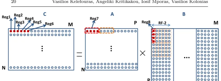
For the reminder of this paper, the three arrays names and sizes are that shown in Fig. 1, i.e.,C =C+A×B, whereC,A andB are of size N×M, N×P andP×M, respectively.
MMM performance depends on the time needed to the i) data to be loaded/stored (C, A and B arrays), ii) matrix operations to be executed, iii) addressing instructions to be executed (integer instructions only), iv) instruc-tions to be loaded from instruction cache.
cache conflicts occur; this is because the MMM code size is small and it always fits in L1 instruction cache. It is important to say that all the todays processors contain separate L1 data and instruction caches and thus we can assume that shared/unified L2/L3 caches, contain only data. Architectures with unified L1 caches are not discussed in this paper.
Eq. 1 and eq. 2 approximate the MMM execution time; eq. 1 holds for architectures that matrix operations and addressing operations are executed in parallel (we assume that the arrays are floating point numbers) and eq. 2 holds for architectures that do not (either no floating point Arithmetic Logic Unit (ALU) exists or the arrays are of type integer); in most architectures the load/store unit and the execution unit work in parallel.
Ttotal=max(Tdata, Tmatrix−operations, Taddressing) (1)
Ttotal=max(Tdata, Tmatrix−operations+Taddressing) (2)
Regarding the time needed to execute the matrix operations (Tmatrix−operations), it is given by the following two equations, i.e., eq. 3 and
eq. 4; eq. 3 is used in the case there is a separate multiplication unit working in parallel with the ALU and eq. 4 otherwise (the number of multiplications is larger than the number of additions).Tmatrix−operationsis a constant number.
Tmatrix−operations=
M ullat×(N×M ×P)
N umM ult
(3)
Tmatrix−operations=
M ullat×(N×M×P)
N umM ult
+Addlat×(N×M×(P−1)) N umALU
(4) where M ullat, Addlat, N umM ult and N umALU are the latencies and the
numbers of the multiplication and ALU units, respectively.
Regarding addressing instructions, the Taddressing value is not a
constant number; it depends on the implementation/schedule. The number
of addressing instructions is decreased when a) the number of the levels of tiling is decreased, b) the tile sizes are increased, c) more array references are assigned into available registers, d) loop unroll factor is increased.
Regarding load/store instructions,Tdata≻Tmatrix−operationsin most
cases, i.e., if the data do not fit in L1 data cache. On the contrast to the Tmatrix−operations, Tdata and Taddressing are not constant numbers; they
de-pend on the schedule used. Also,TdataandTaddressing depend on each other;
normally, by increasing Tdata value, Taddressing is decreased and vice versa,
while the number of the matrix operations remains constant.
To summarize, given that Tmatrix−operations is a constant number and in
most cases Tmatrix−operations ≺ Taddressing and Tmatrix−operations ≺ Tdata,
MMM performance can be increased only by minimizing bothTdataandTaddressing
values; given thatTdataandTaddressing are interdependent, high performance
the separate optimization of the Tdata and Taddressing values, gives different
schedules which cannot coexist, as by refining one, degrading another. Tdatavalue is found by decreasing the search space theoretically according
to the memory hierarchy architecture parameters. For different cache hierarchy architecture, a different equation that estimates Tdata value is created, e.g.,
for one level of data cache architecture Tdata value is given by eq.7. These
equations give theoretically the tile sizes that achieve a minimumTdatavalue.
As far theTaddressing value is concerned, it cannot be found theoretically.
This is because the number of the addressing instructions highly depends on the target compiler and its optimizations, e.g., unroll factor values. Thus, we find all the schedules achieving a lowTdatavalue and only these that achieve a
lowTaddressing value are selected; all the schedules achieving a lowTdatavalue
are converted into assembly code (by using the target compiler) and their number of addressing instructions is measured. Then, all schedules achieving both low Tdata and Taddressing values are compiled and run to the target
platform to find the fastest.
Instead of searching all different MMM schedules to find the best which is impractical because their number is enormous, only a small number is searched. The exploration space is decreased by orders of magnitude since we test only solutions that are close to the best; we test only these schedules achieving both lowTdata andTaddressing values. In this way, the compilation
time is drastically decreased.
A different schedule is emerged for different types of CPUs, CPU param-eters and input size. The reminder of this paper presents all these schedules. The proposed methodology for CPUs with one core is given in subsection 3.1, while the proposed methodology for CPUs with more than one cores is given in subsection 3.2. The proposed methodology for GPU architectures is given in subsection 3.3.
A different schedule is given according to the a) number and the type of the cores, b) number of cache memories, c) cache sizes, d) input sizes and e) whether an SIMD unit is supported or not (Fig. 2). In Fig. 2, ’S’, ’M’ and ’L’ indicate small, medium and large input sizes, respectively. Also, the 3.1.1-3.1.6, 3.2.1, 3.2.2 and 3.3 values that are shown in Fig. 2 refer to the Subsect. 3.1.1 - Subsect. 3.1.6, Subsect.3.2.1, Subsect.3.2.2 and Subsect.3.3, respectively and they are given below.
3.1 CPUs with one core
Single core CPUs
L1 data cache only
L1 data cache and L2 cache
SIMD support
No SIMD support
S M L
Multi core CPUs GPUs
S M L
3.1.6 3.1.1 3.1.6 3.1.2 3.1.6 3.1.3 3.1.1 3.1.1 3.1.2 3.1.1 3.1.3 SIMD support No SIMD support
S M L S M L
3.1.6 3.1.1 3.1.6 3.1.4 3.1.6 3.1.5 3.1.1 3.1.1 3.1.4 3.1.1 3.1.5 Shared L2 Shared L3 3.2.1 3.2.2 3.3
Fig. 2 All different MMM cases. The last nodes refer to the Subsections that provide the appropriate schedules. ’S’, ’M’ and ’L’ indicate small, medium and large input sizes, respectively.
C
N
M
A
N
P
..
.
B
P
M
..
.
..
.
...
...
...
i
0i
0j
0j
0=
X
Tile0
Tile0
Tile0
L1
L1
Fig. 3 MMM for small input sizes and CPU with L1 data cache and with/without L2 cache
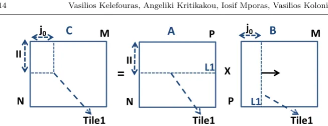
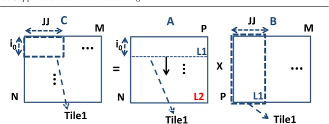
3.1.1 Small input sizes and CPU with L1 data cache and with/without L2 cache
For small input sizes, i.e., if all the data of B, the data of 2×i0 rows of A and
the data of 2×i0 rows of C fit in different ways of L1 data cache (ineq. 5),
the scheduling given below is used (Fig. 3).
L1×(assoc−k1−k2)
assoc ≥P×M×element size, (5) where k1 =⌈2×i0×P×element size
L1/assoc ⌉ ≤ assoc
4 , k2 =⌈
2×i0×M×element size L1/assoc ⌉ ≤ assoc
4 , L1 is the size of the L1 data cache memory in bytes, element size
[image:10.595.81.405.71.317.2] [image:10.595.88.396.364.461.2](assoc6= 1).P×M is the size of the B array in elements.k1 is an integer and it gives the number of L1 data cache lines with identical L1 addresses used for 2×i0rows of A;k2 is an integer and it gives the number of L1 data cache lines
with identical L1 addresses used for 2×i0 rows of C; for the reminder of this
paper we will more freely say that we use k1 cache ways for A, k2 ways for C and (assoc−k1−k2) cache ways for B (in other words A, B and C are written in separate data cache ways). In the case thatP×M ≫2×i0×P+ 2×i0×M
or in the case that a two-way set associative cache exists, 1 cache way is used for both A and C. In the case that assoc= 1, a slightly different schedule is given at the last paragraph of Subsect. 3.1.3.
The optimum production-consumption (when an intermediate result is pro-duced it is directly consumed-used) of array C and the sub-optimum data reuse of array A have been selected by splitting the arrays into tiles according to the number of the registers, eq. 6 (Fig. 3). All different i0, j0 combinations
satisfying ineq. 6 give a feasible solution.
RFF P ≥i0×j0+i0+j0 (6)
where RFF P is the number of the available floating point registers. In the
case that C,A and B contain integer numbers, ineq. 6 contains the addressing variables and the loop iterators.
We use i0×j0 registers for C, i0 for A and j0 for B (Fig. 3). We assign
registers acrossi, jiterators (Fig. 1) and not acrosskiterator becausekis the innermost one (it is changes its value in each iteration and thus no data reuse is achieved).
The schedule is shown in Fig. 3. First, the first i0 elements of the first
column of A are multiplied by the firstj0elements of the first row of B. Then,
the first i0 elements of the second column of A are multiplied by the firstj0
elements of the second row of B etc. This is repeated until the firsti0 rows of
A have been multiplied by the firstj0 columns of B; then the samei0 rows of
A as above, are multiplied by the nextj0 columns of B etc.
Given that each row of A is multiplied by all columns of B, both A and B are reused M and N times, respectively; thus, they have to remain in L1 data cache. To do this, the cache lines of A and B must be written in L1 without conflict with each other and also with C. 2×i0 rows of A and C have to fit
in L1, the current processedi0rows and the next ones, for two reasons. First,
except from the first i0 rows of A and C, also the second i0 rows must be
loaded in L1, without conflict with B. Second, when the thirdi0rows of A are
multiplied by B, the L1 cache lines containing the firsti0rows are replaced by
the thirdi0rows ones according to the LRU cache replacement policy, without
conflict with the B ones. This is achieved by storing the rows of A, C and the columns of B in consecutive main memory locations and by using (k1× L1
assoc)
L1 memory size for A, (k2× L1
assoc) for C and ((assoc−k1−k2)× L1 assoc) for
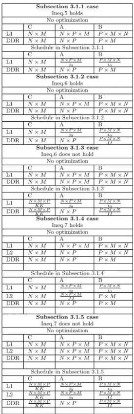
Table 1 Number of data accesses in memory hierarchy
Subsection 3.1.1 case
Ineq.5 holds No optimization
C A B
L1 N×M N×P×M P×M×N
DDR N×M N×P P×M
Schedule in Subsection 3.1.1
C A B
L1 N×M N×P×M j0
P×M×N i0
DDR N×M N×P P×M
Subsection 3.1.2 case
Ineq.6 holds No optimization
C A B
L1 N×M N×P×M P×M×N
DDR N×M N×P P×M×N
Schedule in Subsection 3.1.2
C A B
L1 N×M N×P×M j0
P×M×N i0
DDR N×M N×P P×M×N II Subsection 3.1.3 case
Ineq.6 does not hold No optimization
C A B
L1 N×M N×P×M P×M×N
DDR N×M N×P×M P×M×N
Schedule in Subsection 3.1.3
C A B
L1 N×M×P KK
N×P×M j0
P×M×N i0
DDR N×M×P KK N×P
P×M×N II Subsection 3.1.4 case
Ineq.7 holds No optimization
C A B
L1 N×M N×P×M P×M×N
L2 N×M N×P P×M×N
DDR N×M N×P P×M
Schedule in Subsection 3.1.4
C A B
L1 N×M N×P×M j0
P×M×N i0
L2 N×M N×P×M
J J P×M
DDR N×M N×P P×M
Subsection 3.1.5 case
Ineq.7 does not hold No optimization
C A B
L1 N×M N×P×M P×M×N
L2 N×M N×P×M P×M×N
DDR N×M N×P×M P×M×N
Schedule in Subsection 3.1.5
C A B
L1 N×M×P KK
N×P×M j0
P×M×N i0
L2 N×M×P KK
N×P×M j0
P×M×N II
DDR N×M×P KK N×P
P×M×N II
the size of the cache) of A, C and B memory addresses. It is important to say that if we useL1≥(P×M+ 2×i0×P+ 2×i0×M)×element sizeinstead
of ineq. 5, the number of L1 misses will be much larger because A, B and C cache lines would conflict with each other.
Tdata=max(
L1load lat×L1loads+L1store lat×L1stores
L1ports
,
DDRload lat
lineL1
×DDRloads+DDRstore lat×
DDRstores× ⌈j0/lineL1⌉
j0
) (7)
where L1load lat, DDRload lat, L1store lat, DDRstore lat are the L1 and
DDR load and store latencies, respectively.L1loads,DDRloads,L1stores,DDRstores,
are the numbers of loads and stores occur for each memory and they are shown in Table 1.lineL1 is the number of elements each L1 cache line contains and
L1ports is the number of L1 load/store ports. Without loss of generality, in
eq. 7, we assume a memory architecture that only one L1 cache line is re-placed at a time; if more than one cache lines are rere-placed in parallel, then eq. 7 is changed accordingly.
Regarding the number of DDR writes,⌈j0/lineL1⌉L1 data cache lines are
written to main memory for eachj0elements of C. For data cache architectures
where reads and writes are executed in parallel, eq. 7 is changed accordingly. From eq. 7 and Table 1, we can approximate the Tdata value. Supposing
that L1 and DDR load/store latencies are 1 and 50, respectively and also that L1ports= 1 andlineL1= 4, eq. 7 and Table 1 give
Tdata=max(2×N×M +
N×P×M i0
+P×M ×N j0
,
50
4 ×(N×M+N×P+P×M) + 50×
N×M × ⌈j0
4⌉
j0
) (8)
Regarding DDR access time, it is minimized whenj0is a multiple of cache
line size, i.e., 4. Regarding L1 data cache access time, it is minimized when (1
i0 +
1
j0) is minimized (i0, j0 are found according to ineq. 6 and RFF P is a
power of 2). For RFF P = 8 orRFF P = 16, the above equation is minimized
when i0 == j0. Let us consider that there are 16 floating point registers. If
i0 == j0, then i0 = j0 = 3 and the number of L1 data cache accesses is
N ×M +2N M P
3 , while if i0 = 1 and j0 = 14, the number of L1 data cache
accesses is N ×M +15N M P14 ≻ N ×M +2N M P3 . Also, if RFF P = 8, then
i0 =j0 = 2 gives the minimum L1 data cache access time. However, in the
case that RFF P = 32, we cannot find a goodi0 =j0 solution, since several
registers are wasted, i.e., ifi0=j0= 4 then 16, 4 and 4 registers are used for
C, A and B, respectively, which means that only 24/32 registers are used; in this case, we do not fully utilize the RF size and thus a solution different than i0 =j0 is preferred, e.g.,i0 = 5 and j0 = 4. On the other hand, if we select
i0=j0= 5, then we need 35 register which are more than 32.
However, the best performance is not always achieved by minimizingTdata
value; although i0 ==j0 case achieves a lower number of data accesses than
for(i=0; i<N; i+=2) {
for (j=0; j<M; j+=2) {
r1=0;r2=0;r3=0;r4=0;
for (k=0; k<P; k++) {
r5=A[i][k]; r6=A[i+1][k];
r7=B[k][j]; r8=B[k][j+1];
r1+=r5*r7; r2+=r5*r8; r3+=r6*r7; r4+=r6*r8;
} C[i][j]=r1; C[i][j+1]=r2; C[i+1][j]=r3; C[i+1][j+1]=r4; } }
for(i=0; i<N; i++) {
for (j=0; j<M; j+=6) {
r1=0;r2=0;r3=0;r4=0;r5=0;r6=0;
for (k=0; k<P; k++) {
r7=A[i][k];
r8=B[k][j];
r1+=r7*r8; r8=B[k][j+1];
r2+=r7*r8; r8=B[k][j+2];
r3+=r7*r8; r8=B[k][j+3];
r4+=r7*r8; r8=B[k][j+4];
r5+=r7*r8; r8=B[k][j+5];
r6+=r7*r8; }
C[i][j]=r1; C[i][j+1]=r2; C[i][j+2]=r3; C[i][j+3]=r4; C[i][j+4]=r5; C[i][j+5]=r6; } }
(a) (b)
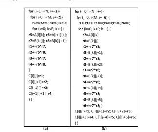
Fig. 4 MMM optimized code forRFF P = 8. In (a)i0=j0= 2, while in (b)i0= 1 and
j0= 6. (a) achieves a lowerTdatavalue but (b) achieves a lowerTaddressingvalue
addressing instructions; this is because in the first case, more array addresses per iteration, are computed (Fig. 4).
The above schedule achieves the minimum number of data accesses (for the most register file sizes). In this case, C array is loaded and stored once from L1 data cache, while A and B are loaded N/i0 and M/j0, respectively
(for square matrices, N2 stores and N2+N3/i0+N3/j0 loads occur). The
row-column way of multiplying is the best. If we use another schedule, e.g., loop interchange transformation is applied and the iterators arek, i, j, instead ofi, j, kand thus we usei0×j0,i0andj0registers for A, C and B, respectively,
thenN3/i
0stores andN2+N3/i0+N3/j0 loads occur, which are more than
those in the previous case. A larger number of data accesses occurs because C is always accessed twice (C array is both loaded and stored); thus, it is more efficient to access C array once and A, B arrays more times, than the opposite.
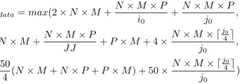
3.1.2 Medium input sizes with L1 data cache only
For medium input sizes where ineq. 9 holds, another schedule is used (Fig. 5). If all the data of a Tile1 of A and a Tile1 of B fit in separate ways of L1 cache (ineq. 9), the scheduling given below is used.
L1×(assoc−k)
[image:14.595.75.400.74.344.2]C
N
M
A
N
P
B
P
M
j
0II
j
0=
X
Tile1
Tile1
Tile1
II
L1
L1
Fig. 5 MMM for medium input sizes and CPUs with L1 data cache only
where k = ⌈P×j0×element size L1/assoc ⌉ ≤
assoc
2 , L1 is the size of the L1 cache,
associs the L1 associativity (assoc6= 1) and element size is the size of the arrays elements in bytes.
kis an integer and it gives the number of L1 data cache lines with identical L1 addresses used for Tile1 of B; we use k cache ways for B and assoc−k cache ways for A (in other words A and B are written in separate data cache ways).
In order to the Tile1 tiles of A and B remain in L1 data cache, the cache lines of Tile1 of A must be written in L1 without conflict with the Tile1 of B ones. This is achieved by storing the Tile1 of A and the Tile1 of B in consecutive main memory locations and by using (k×assocL1 ) L1 memory size for B and ((assoc−k)× L1
assoc) L1 memory size for A (ineq. 9). We can more
freely say that this is equivalent to usingkcache ways for B and (assoc−k) cache ways for A. An empty cache line is always granted for each different modulo (with respect to the size of the cache) of A and B memory addresses. We do not need any empty space for C because a) Tile1 of C size is much smaller than the other Tile1 tiles (normally,P ≫II ≻j0), b) each element of
C is stored just once into memory (no data reuse) and c) C is stored into main memory infrequently; thus, the number of conflicts due to C can be neglected (victim cache if exists, eliminates the misses of C). However, ifP is comparable toII, then an additional cache way must be used for C.
Ineq. 9 holds only when Tile1 of A and B are written in consecutive main memory locations. Given that the arrays are written row-wise in main memory, the elements of Tile1 of A are written in consecutive main memory locations, but the elements of Tile1 of B are not. Thus, the data layout of B is changed from row-wise to tile-wise, i.e., all elements are written in main memory just as they are fetched; first, the firstj0elements of the first row of B are written
to main memory, then the firstj0 elements of the second row of B etc.
It is important to say that if we useL1≥(II×P+P×j0)×element size
instead of ineq. 9, the number of L1 misses will be much larger because A and B cache lines would conflict with each other.
The scheduling follows. First, the first i0 rows of A are multiplied by the
firstj0 columns of B exactly as in the previous subsection. Then the nexti0
[image:15.595.74.401.66.192.2]C
N
M
A
N
P
B
P
M
KK
j
0II
II
j
0KK
=
X
Tile1
Tile1
Tile1
L1
L1
Fig. 6 MMM for large input sizes and CPUs with L1 data cache only
until all the rows of Tile1 of A are multiplied by the first j0 columns of B.
After the first Tile1 of A has been multiplied by the first Tile1 of B, the first Tile1 of A is multiplied by the second Tile1 of B etc. In this way, data reuse is achieved on both A and B arrays.
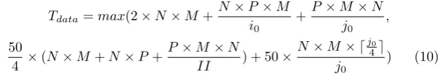
[image:16.595.76.408.72.195.2]The time needed for the arrays elements to be loaded/stored, is approxi-mated by eq. 7 and Table 1. Supposing that L1 and DDR load/store latencies are 1 and 50, respectively and also thatL1ports= 1 andlineL1= 4, eq. 7 and
Table 1 give
Tdata=max(2×N×M +
N×P×M i0 +
P×M ×N j0 ,
50
4 ×(N×M +N×P+
P×M ×N
II ) + 50×
N×M× ⌈j0
4⌉
j0
) (10)
Regarding DDR access time, it is minimized whenII is maximized andj0
is a multiple of cache line size, i.e., 4; alsoIIis maximized whenj0= 1 (IIand
j0 are interdependent); there is a trade-off. Regarding L1 data cache access
time, it is minimized when (1 i0 +
1
j0) is minimized (i0, j0 are found according
to ineq. 6).
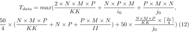
3.1.3 Large input sizes and CPUs with L1 data cache only
For large input sizes, where ineq. 9 does not hold, the scheduling given below is used (Fig. 6).
In this case, i0 rows of A and j0 columns of B do not fit in L1; ineq. 9
cannot givej0≻1 andi0≻1. Thus, P dimension is also tiled and Tile1 tiles
become even smaller; Tile1 tiles containi0sub-rows of A and j0sub-columns
of B; the Tile1 tiles of A and B are of sizeII×KK andKK×j0, respectively.
KK is selected to be as large as possible since C array is both loaded and stored,KK times from main memory.
[image:16.595.95.408.342.395.2]L1×(assoc−k)
assoc ≥II×KK×element size (11)
where k = ⌈j0×KK×element size
L1/assoc ⌉ ≤
assoc
2 , KK =
P 1,
P 2, ...,
P
n and n is
positive integer (n≥1).
IIsub-rows of A andj0sub-columns of B of sizeKK, have to fit in separate
ways of L1 data cache. It is important to say that ineq. 11 holds only when the tile elements of A and B are written in consecutive main memory locations; otherwise, the tile sub-rows/sub-columns will conflict with each other due to the cache modulo effect. As it was explained in the previous Subsection, we do not need any empty space for C. However, if the size of Tile1 of C is comparable to the others, then cache size which equals to one cache way must be granded for C.
Regarding the data layout of A, when P dimension is tiled, the data layout of A is changed from row-wise to tile-wise; A elements are written into memory just as they are fetched. If the data layout of A is not changed, ineq. 11 cannot give a minimum number of cache conflicts since the sub-rows of A will conflict with each other. The same holds for B. The data array layout of B is changed from row-wise to tile-wise.
The scheduling follows. The multiplication between two Tile1 tiles is ex-actly the same as in the previous case (Subsection 3.1.1). First, the first Tile1 of A is multiplied by all Tile1 tiles of the first Tile1 block row of B. Then, the second Tile1 of the first Tile1 block column of A is multiplied by all the Tile1 tiles of the first Tile1 block row of B. Then, the second Tile1 block column of A is multiplied by the second Tile1 block row of B etc.
[image:17.595.88.410.469.526.2]The time needed for the array elements to be loaded/stored, is approxi-mated by eq. 7 and Table 1. Supposing that L1 and DDR load/store latencies are 1 and 50, respectively and also thatL1ports= 1 andlineL1= 4, eq. 7 and
Table 1 give
Tdata=max(
2×N×M ×P
KK +
N×P×M i0
+P×M ×N j0
,
50 4 ×(
N×M×P
KK +N×P+
P×M×N
II ) + 50×
N×M×P
KK × ⌈
j0
4⌉
j0
) (12)
Regarding DDR access time, it is minimized when KK andII are maxi-mized and whenj0is a multiple of cache line size, i.e., 4.Tdatahighly depends
on the KK and II values which are the largest possible according to the L1 data cache size.
In the case of direct mapped data cache, both A and B tiles compete with each other for the same L1 addresses. Given that both tiles cannot remain in L1 due to the cache modulo effect, we select Tile1 of A to be many times larger than Tile1 of B, i.e., II ≫j0. In this way, the main part of Tile1 of A
C
N
M
A
N
P
B
P
M
...
i
0i
0JJ
...
L1
L1
L2
Tile1
Tile1
Tile1
=
..
.
X
...
JJ
Fig. 7 MMM for medium input sizes and CPUs with L2 and L1 data cache
3.1.4 Medium input sizes and CPUs with L2 and L1 data cache
If all the data of A and the Tile1 of B/C fit in separate ways of L2 cache (ineq. 13), the scheduling given below is used (Fig. 7).
L2×(assoc−1)
assoc ≥N×P×element size (13) where L2 is the size of the L2 cache, assoc is the L2 associativity and element sizeis the size of the arrays elements in bytes (e.g.,element size= 4 for floating point numbers).
Given that N ≫JJ for most cases, the size of A is much larger than the size of Tile1 of B and Tile1 of C, and thus ((assoc−1)×assocL2 ) and (assocL2 ) L2 size is needed for A and B-C arrays, respectively.
Regarding L1 data cache, 2×i0 rows of A and JJ columns of B have to
fit in separate ways of L1 (ineq. 14).
L1×(assoc−k)
assoc ≥P×JJ×element size, (14)
where k = ⌈2×i0×P×element size
L1/assoc ⌉ ≤ assoc
2 , L1 is the size of the L1 data
cache memory in bytes, element size is the size of the arrays elements in bytes andassocis the L1 associativity (assoc6= 1).
The scheduling follows. First, the first Tile1 of A is multiplied by the first Tile1 of B. The multiplication between two Tile1 tiles is the same as in Subsect. 3.1.1. Then, the second Tile1 of A is multiplied by the same Tile1 tiles of B as above etc. We select the whole A to fit in L2, since having a Tile1 of B in L1 data cache, its elements need to be multiplied by as many rows of A as possible before they are spilled to upper level memories.
The time needed for the array elements to be loaded/stored, is approxi-mated by eq. 19 and Table 1.
Tdata=max(L1load lat×L1loads+L1store lat×L1stores
L1ports
[image:18.595.80.409.74.198.2]L2load lat
lineL1
×L2loads+L2store lat×
L2stores× ⌈j0/lineL1⌉
j0
,
DDRload lat
lineL2
×DDRloads+DDRstore lat×DDRstores× ⌈j0/lineL2⌉
j0
)(15)
whereL1load lat,L2load lat,DDRload lat,L1store lat,L2store lat,DDRstore lat
are the L1,L2 and DDR load and store latencies, respectively.L1loads,L2loads,
DDRloads,L1stores,L2stores,DDRstores, are the numbers of loads and stores
occur for each memory, according to Table 1.lineL1/lineL2 are the numbers
of elements each L1/L2 cache line contains and L1ports is the number of L1
load/store ports. In eq. 7, we assume that only one L1/L2 cache line is replaced at the time; if more than one cache lines are replaced concurrently, e.g., two lines, then eq. 7 is changed accordingly.
[image:19.595.122.360.291.375.2]Supposing that L1, L2 and DDR load/store latencies are 1, 4 and 50, respectively and also that L1ports = 1, lineL1 = 4, lineL2 = 4, eq. 7 and
Table 1 give
Tdata=max(2×N×M+
N×M×P i0
+N×M×P j0
,
N×M+N×M×P
JJ +P×M+ 4×
N×M× ⌈j0
4⌉
j0
,
50
4 (N×M +N×P+P×M) + 50×
N×M× ⌈j0
4⌉
j0
) (16)
Regarding DDR access time, it is minimized when j0 is a multiple of L2
cache line size, i.e., 4. Regarding L2 data cache access time, it is minimized whenJJ is maximized and j0is a multiple of L1 cache line size, i.e., 4. JJ is
maximum according to the L1 data cache size. Regarding L1 data cache access time, it is minimized when (1
i0 +
1
j0) is minimized.
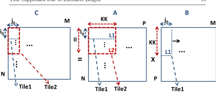
3.1.5 Large input sizes and CPUs with L2 and L1 data cache
For large input sizes, where ineq. 13 does not hold, the scheduling given below is used (Fig. 8).
In this case, ineq. 14 cannot giveJJ≻1 andi0≻1. Thus, P dimension is
also tiled as in Subsect. 3.1.3 and Tile1 tiles become even smaller.
Thus, instead of multiplying rows of A by columns of B, sub-rows of size KK are multiplied by sub-columns of sizeKK. The Tile1 of A becomes of size i0×KK and the Tile1 of B becomes of sizeKK×j0; the largestj0 integer
value for KK = P/2 is selected that ineq. 17 holds. If ineq. 17, still cannot give aj0 value satisfying ineq. 6,KK =P/3 is selected and etc.
L1×(assoc−k)
assoc ≥KK×j0×element size (17) where k = ⌈2×i0×KK×element size
L1/assoc ⌉ ≤
assoc
2 , KK =
P 1,
P 2, ...,
P
n and n is
C
N
M
A
N
P
B
P
M
j
0i
0i
0j
0...
L1
L1
L2
Tile2
Tile1
Tile1
Tile1
II
KK
KK
Tile2
=
X
..
.
..
.
..
.
...
...
...
Fig. 8 MMM for large input sizes and CPUs with L2 and L1 data cache
2×i0 sub-rows of A and j0 sub-columns of B of size KK, have to fit in
separate ways of L1 data cache. It is important to say that ineq. 17 holds only when the tiles of A and B are written in consecutive main memory locations (tile-wise); otherwise, the tiles sub-rows/sub-columns will conflict with each other due to the cache modulo effect.
To efficiently use the L2 cache, the array A is further partitioned intoT ile2 tiles. AT ile2 tile of A (size ofII×KK), a Tile1 tile of B (size ofKK×j0) and
a Tile2 of C (size ofII×j0), have to fit in L2 cache (ineq. 18). Array A uses
assoc−1 L2 ways while B-C arrays use only one L2 way. This is because the sum of Tile2 of C and Tile1 of B, is of smaller size than one L2 way (II≫j0);
moreover, C and B tiles do not achieve data reuse in L2 and thus there is no need to remain in L2 (Tile1 of B is reused in L1 data cache not in L2).
L2×(assoc−1)
assoc ≥II×KK×element size (18) The scheduling follows. First, the first Tile1 of the first Tile2 of A is multi-plied by the first Tile1 of the first Tile1 block row of B. Then, the second Tile1 of the first Tile2 of A is multiplied by the same Tile1 of B as above etc. After the first Tile2 of A has been multiplied by the first Tile1 of B, it is multiplied by the remaining Tile1 tiles of the first Tile1 block row of B. Then, the second Tile2 of the first Tile2 block column of A is multiplied by the all Tile1 tiles of the first Tile1 block row of B etc. The procedure ends when all Tile2 block columns of A have been multiplied by all Tile1 block rows of B.
We select a big Tile2 of A to fit in L2, since a Tile1 of B which resides in L1 data cache, is multiplied by all rows of A; thus we multiply Tile1 of B with as many rows of A as possible before they are spilled to the upper level memory.
The time needed for the array elements to be loaded/stored, is approx-imated by eq. 19 and Table 1. Supposing that L1, L2 and DDR load/store latencies are 1, 4 and 50, respectively and also that L1ports= 1, lineL1 = 4,
[image:20.595.56.426.72.229.2]C A B
...
RF-2 M
P P
N N
M
..
.
Reg7
Reg8 Reg1 Reg2
Reg3Reg4Reg5 Reg6
..
.
Fig. 9 MMM for CPUs with SIMD
Tdata=max(
2×N×M
KK +
N×M×P i0
+N×M×P j0
,
N×M×P
KK +
N×M×P j0
+P×M ×N II + 4×
N×M×P
KK × ⌈
j0
4⌉
j0
,
50 4 (
N×M ×P
KK +N×P+
N×M×P
II ) + 50×
N×M×P
KK × ⌈
j0
4⌉
j0 ) (19)
3.1.6 CPUs with SIMD
In this case, a scheduling similar to that explained in Subsect. 3.1.1 is used. The optimum production-consumption (when an intermediate result is produced it is directly consumed-used) of array C and the sub-optimum data reuse of array A have been selected by splitting the arrays into tiles according to the number of XMM/YMM registers (eq. 20).
RF =p+ 1 + 1 (20)
whereRF is the number of the XMM/YMM registers andpis the number of the registers used for C array. Thus, we assignpregisters for C and 1 register each for A and B.
Regarding Tdata value, the best schedule here is similar to than given in
Subsect. 3.1.1, i.e., 2×2, 2 and 2 registers are used for C, A and B, when RF = 8 and 3×3, 3 and 3 registers are used for C, A and B, whenRF = 16. However, the schedule according to ineq. 20 is faster on SIMD architectures since the lower number of addressing instructions has a larger effect on per-formance. As thepvalue increases, the number of SSE instructions decreases (it is explained below). We have evaluated both solutions in a large number of different architectures and the first (that of Fig. 9) is the fastest at all architectures.
[image:21.595.53.431.69.207.2]data (4 byte elements). The first 4 elements of the first row of A (A(0,0 : 3)) and the first four elements of the first column of B (B(0 : 3,0)) are loaded from memory and they are assigned into XMM0 and XMM1 registers respectively (the elements of B have been written into main memory tile-wise, i.e., just as they are fetched). XMM0 is multiplied by XMM1 and the result is stored into XMM2 register (Fig. 4). Then, the next four elements of B (B(0 : 3,1)), are loaded into XMM1 register again; XMM0 is multiplied by XMM1 and the result is stored into XMM3 register (Fig. 9, Fig. 4). The XMM0 is multiplied by XMM1 for 6 times and the XMM2:XMM7 registers contain the multipli-cation intermediate results of the C array. Then, the next four elements of A (A(0,4 : 7)) are loaded into XMM0 which is multiplied by XMM1 for 6 times, as above (Fig. 4); the intermediate results in XMM2:XMM7 registers, are al-ways produced and consumed. When the 1st row of A has been multiplied by the first 6 columns of B, the four values of each one of XMM2:XMM7 registers are added and they are stored into main memory (C array), e.g., the sum of the four XMM2 values, isC(0,0).
The above procedure continues until all the rows of A have been multiplied by all the columns of B. There are several ways to add the XMM2:XMM7 data; three of them are shown in Fig. 10, where 4 XMM registers are used to store the data of C, i.e., XMM1, XMM2, XMM3 and XMM4 (the SSE instructions’ latencies are taken into account here). The first one (Fig. 10-a) sums the four 32-bit values of each XMM register and the results of the four registers are packed in one which is stored into memory (the four values are stored into memory using one SSE instruction). The second one, sums the four 32-bit values of each XMM register and then each 32-bit value is stored into memory separately (without packing). For most SIMD architectures, the second (Fig. 10-b) is faster than the first one, because the store and add operations can be executed in parallel (the first one has a larger critical path). The third one (Fig. 10-c), unpacks the 32-bit values of the four registers and packs them into new ones in order to add elements of different registers. For most SIMD architectures, the third is faster than the other two ones, because unpacking and shuffle operations usually have smaller latency and throughput values than slow hadd operations.
By using SSE instructions, eq.1 changes into eq. 21. KK is not shown in Fig. 9;KKis the tile size across dimension P and for large input sizesKK ≺P (Fig. 8). As theKK value decreases, the number of SSE instructions increases according to the following equation (code shown in Fig. 10 is executed more times).
Ttotal=max(Tdata, Tmatrix−operations+c×
N×M ×KKP
p , Taddressing) (21)
a)
b)
c)
Fig. 10 Three different ways for unpacking the multiplication results using SSE intrinsics; XMM1, XMM2, XMM3, XMM4 contain the C values. For most SIMD architectures, the three schedules are in increased performance order.
3.2 Multi-core CPUs
To run MMM effectively in many cores, the MMM problem is partitioned into smaller sub-problems and each sub-problem corresponds to a thread; each thread runs in one core only. Each thread must contain at least p1 instruc-tions, wherep1 is found experimentally and differs from one CPU to another. Otherwise, the cores will remain several CPU cycles idle since the threads initialization and synchronization time is made comparable to the threads ex-ecution time; this leads to low performance. Furthermore, in order to achieve high performance, the number of the threads must be higher thanp2, where p2 is found experimentally. The impact ofp1 andp2 on performance is com-parable to the memory management problem.
Regarding small input sizes, a large speedup cannot be achieved. This is because either a low p1 and/or a low p2 value is selected. In this case it is preferable to run MMM in fewer number of cores in order to increase p1 and/orp2.
C A B
KK
... ... ... ...
...
...
...
..
.
..
.
K
K
JJ
j0
II
core_0 core_1 core_2 core_3
core_0 core_1 core_2 core_3
Tile2 Tile1
...
...
JJJ
II
JJ
P
P
M
N N
M
..
.
...
[image:24.595.55.433.74.249.2]Tile2 Tile2
Fig. 11 The proposed methodology for 4 cores having a shared L2 cache.
Ttotal=max(Ttotal−core1, Ttotal−core2, Ttotal−core3, Ttotal−core4) (22)
Ttotal−corei=
N um−ofX−T hreads
j=1
Ttotal−threadj (23)
where i= [1,4] andTtotal−threadj is theTtotal value given in Subsect. 3.1.
Most multi core processors, typically contain 2 or 3 levels of cache, i.e., a) separate L1 data and instruction caches and a shared L2 cache, b) separate L1 data and instruction caches, separate unified L2 caches and a shared L3 cache. The proposed methodology for shared L2 and shared L3, is given in Subsect. 3.2.1 and Subsect. 3.2.2, respectively.
3.2.1 CPUs with shared L2
To utilize L2 shared cache, we partition the three arrays into Tile2 tiles (Fig. 11). The Tile2 tiles of A, B and C, are of size II ×KK, KK ×JJ and II ×JJ, respectively. Each multiplication between two Tile2 tiles cre-ates a different thread. For small and medium input sizes, we always select KK =P (Fig. 11). Each multiplication between two Tile2 tiles is made as in Subsect. 3.1.5. Havingq number of cores, each Tile2 of A is multiplied by q consecutive Tile2 tiles of B in parallel, each one at a different core (Fig. 11); thus,JJJ (JJJ=q×JJ) is evenly divisible byM.
withassoc≥q+ 1 is needed here. Cache size equal to ((assoc−q)×assocL2 ) and (q×assocL2 ) is needed for A (array A is written into main memory tile-wise) and B-C, respectively (ineq. 24). We select a big Tile2 of A to fit in L2 since having one Tile1 of B in each one of theqL1 data caches, their elements need to be multiplied by as many rows of A as possible before they are spilled to L2; Tile2 of A is reusedM/j0times. L2 cache size that equals toqL2 ways is
used for the Tile1 tiles of B and C, since their size is small and their elements are not reused (Tile1 of B is reused in L1 data cache not in L2).
Regarding L2 data cache, the largest II value which satisfy ineq. 24 is selected (Fig. 11). Given that a Tile1 of B is written in L1 data cache, it is memory efficient to be multiplied by as many rows of A as possible, before it is spilled from L1.
L2×(assoc−q)
assoc ≥II×KK (24)
where theKKvalue is determined according to L1 data cache size (ineq. 17). JJ value depends on the number of instructions each thread must contain and it is found experimentally; ifJJ is smaller than this minimum number, thread initialization and synchronization time is comparable with its execution time. The large number of ways needed here is not a problem as the L2 associativity is larger or equal to 16 in most architectures.
The scheduling follows; suppose that there are four cores (Fig. 11). Each Tile2 of A is multiplied by a Tile2 of B exactly as in Subsect. 3.1.5. Each multiplication between two Tile2 tiles makes a different thread and each thread is executed at only one core. First, the first Tile2 of the first Tile2 block column of A is multiplied by all Tile2 tiles of the first Tile2 block row of B (M/JJ different threads); all M/JJ threads are executed in parallel exploiting the data reuse of Tile2 of A. Then, the second Tile2 of the first Tile2 block column of A is fetched and it is multiplied by all the Tile2 of the first Tile2 block row of B as above, etc. The procedure ends when all Tile2 block columns of A have been multiplied by all Tile2 block rows of B. Concerning main memory data accesses, A, B and C arrays are accessed 1, N/II and P/KK times, respectively.
3.2.2 CPUs with shared L3
To utilize L3 cache, A and B arrays are further partitioned into Tile3 tiles, of size ((q×II)×KK) and (KK×JJJ), respectively (Fig. 12). For small and medium input sizes, we always selectKK =P (Fig. 12). Each multiplication between two Tile2 tiles of A and B makes a different thread. Each multipli-cation between two Tile2 tiles is made as in Subsect. 3.1.5. We determine the Tile1, Tile2 and Tile3 parameters by the data cache sizes and associativities. Regarding L2 cache, we compute the II value according to the L2 archi-tecture parameters (ineq. 25).
L2×(assoc−1)
C A B Tile2 KK ... ... ... ...
...
...
.. . K K JJ II co re 0 Tile2...
...
JJJ II JJ P P M N N M...
...
.. . Tile2 .. . .. . .. . co re 1 co re 2 co re 3 co re 0 co re 1 co re 2 co re 3 Tile3 Tile3 j0Fig. 12 The proposed methodology for 4 cores having a shared L3 cache.
The largestII value is selected satisfying ineq. 25.JJ is found experimen-tally since each thread has to contain a minimum number of instructions.KK is found according to the L1 data cache size (ineq. 17).
Given that a Tile1 of B is written in L1 data cache, it is memory efficient to be multiplied by as many rows of A as possible, before it is spilled from L1. Thus, L2×(assoc−1)
assoc size of L2 is used for A; the layout of A is tile-wise here.
L2 cache size that equals to one L2 way is used for the Tile1 of B and C, since their size is small and their elements are not reused (Tile1 of B is reused in L1 data cache not in L2).
It is important to say that tiling for L2 is not always performance efficient because a) an L2 miss has a small penalty here; this is because in this case, the data are loaded not from main memory but from L3 cache, which is fast enough, b) extra addressing instructions are inserted which may degrade per-formance. Thus, tiling only for L1 and L3, may be more efficient in several cases.
Regarding L3 cache, we compute JJJ according to the L3 cache param-eters. We choose the biggest Tile3 of B possible, to fit in L3 shared cache. There is ((assoc−k−1)× L3
assoc) L3 size for the Tile3 of B, (k× L3
assoc) for A
and (assocL3 ) for C (ineq. 26).
((assoc−k−1)× L3
assoc)≥KK×JJJ (26)
where k=⌈q×II×KK
L3/assoc ⌉and L3 is the size of the L3 cache. The largerJJJ
value is selected satisfying ineq. 26. Also,JJJ=l×JJ wherel is an integer. JJ value depends on the number of instructions, each thread must contain and it is found experimentally.KK value is found according to L1 data cache size and it is given by ineq. 17.
C A B
...
...
...
P
P
M
N N
M
...
SM0SM0 k
k
nk
k
k nk
Tile2 Tile2
Fig. 13 MMM for GPU. The bullets with the red color show the elements ac-cessed/multiplied by Thread0 only.
of Tile3 of B must not conflict with Tile3 of A ones. Cache size equals to one L3 way is used for C array for its cache lines not to conflict with the Tile3 of A and B ones; C elements are not reused and they are not occupying a large space.
The scheduling follows; suppose that there are 4 cores (Fig. 12). Each Tile2 of A is multiplied by a Tile2 of B exactly as in Subsect. 3.1.5. Each multiplication between two Tile2 tiles makes a different thread and each thread is executed in one core only. First, all Tile2 tiles of the first Tile3 of A are multiplied by all Tile2 tiles of the first Tile3 of B ((JJJ/JJ)×q different threads); these threads are executed in parallel exploiting the data reuse of Tile1 of B in L1, the data reuse of Tile2 of A in L2 and the data reuse of Tile3 of B in L3. Then, the same Tile3 of B as above, is multiplied by all the Tile2 tiles of the second Tile3 of the first Tile3 block column of A, etc; each Tile3 of B is reused N/II times (this is why the Tile3 of B has to fit in L3 shared cache) and each Tile2 of A is reused (JJJ/j0) times in L2 (this is why Tile2
of A has to fit in L2 cache). The procedure is repeated until all Tile3 block columns of A have been multiplied by all Tile3 block rows of B.
3.3 GPUs
Regarding MMM performance on GPUs, the most critical parameters are the number of the threads run in parallel, the number of the SMs work in parallel, the GPU occupancy and the memory management.
Table 2 Number of data accesses in memory hierarchy
C A B
shared L1 0 r×n×k2×P
coresSM r×n×P
L1 data cache n2×k2
coresSM 0 0
L2 N×M N×P×M
n×k
P×M×N n×k
DDR N×M N×P×M
n×k
P×M×N n×k
The proposed methodology gives a different schedule according to the GPU architecture parameters and to the input size.
Likewise Subsect. 3.1.1, the best schedule here is that of row-column for two reasons. First, this schedule gives the minimum number of DDR accesses. This is because C array is not just loaded, but it is also stored into main memory (it is accessed twice); thus it is preferable to access C array only once and A, B more times than the opposite (Subsect. 3.1.1). Second, by writing the C array just once to main memory, we avoid synchronization problems and all threads run in parallel.
To utilize the lower level GPU memories, the three arrays are partitioned into smaller ones according to the number of the registers and the number of the threads, each SM supports. The three arrays are partitioned into square tiles of size k×k, where k is a power of 2 and k2 ≤ N um T hreads, where
N um T hreadsis the number of the threads each SM supports. Furthermore, n1 Tile1 tiles of A and n2 Tile1 tiles of B constitute a Tile2 of A and B, respectively (Fig. 13); we selectn=n1 =n2 andn≥2 (a detailed analysis is given below).ndepends on the input size and its maximum value is limited to the number of the available registers. A differentnvalue is selected for different input sizes in order to achieve high occupancy (it is explained below).
The number of blocks of threads run in parallel is N k×n×
M
k×n. In order to
none of the SMs remains idle, ineq. 27 holds. Ineq. 27 satisfies that the number of the blocks of threads is always larger or equal to the number of the SMs; otherwise, several SMs will remain idle.
N×M
k2×n2 ≥N um SM s (27)
We select the largestkvalue possible satisfying ineq. 27, wheren≥2. We select the largestkvalue as by increasingk, a) the number of the threads run in parallel increases, b) the number of data accesses is decreased; in modern GPU architectures, alwaysk≥16.
The schedule follows. There are kN×n ×
M
k×n blocks of threads and each
block containsk2threads. The bullets shown with the red color in Fig. 13, are
and thus there are 9 intermediate results of C (the intermediate results are produced and consumed since they are in registers). The thread1 multiplies the 3 elements of A shown in Fig. 13 by the 3 elements of B that exist by one position to the right of that shown in Fig. 13. The thread2 multiplies the 3 elements of A shown in Fig. 13 by the 3 elements of B that exist by two positions to the right of that shown in Fig. 13 etc. The thread of number k, multiplies the 3 elements of A that exist one position down to those shown in Fig. 13 by the 3 elements of B shown in Fig. 13 etc. In general, each thread multipliesnelements of the first column of Tile2 of A bynelements of the first row of Tile2 of B (k2 threads are executed in parallel). Then the procedure
continues with the second column of Tile2 of A and the second row of Tile2 of B etc. The multiplication of the firstn×krows of A by the firstn×kcolumns of B takes place in the first SM. The multiplication of the firstn×krows of A by the secondn×kcolumns of B takes place in the second SM etc.
The number of data accesses in memory hierarchy is given in Table 3, where r = (kN×n ×
M
k×n)/(N umber SM s) and coresSm is the number of the
cores in each SM (in Table 3, we assume that none of the cores remains idle). In Table 3, the Shared L1 and the L1 data cache value corresponds to each core.
Tile2 tiles of A and B achieve data reuse and thus they are placed in Shared L1 (ineq. 28).
Shared L1≥2×n×k2 (28)
We use shared L1 and not L1 data cache. An implementation with Shared L1 is faster than L1 data cache because a) shared memory normally has 32 banks and is much less susceptible to conflicts, b) by using shared memory, the layout of A and B is not changed (except from special case explained below), decreasing the number of load/store and addressing instructions.
Shared L1 is fully utilized. Shared L1 access time equals to 1 clock if no data conflicts occur. Normally, shared L1 memory is organized into 32 banks and each bank has width of 32 bits; successive 32-bit words are assigned to successive banks. If all threads of a warp access different banks, there is no bank conflict. For most GPU architectures, ifk≥16 no bank conflicts exist. On the other hand, ifk ≺16, the data array layouts are changed from row-wise to tile-row-wise in order to eliminate L1 conflicts, i.e., first we write the first tile’s elements in main memory in the exact order they are loaded, then the second’s etc.
To sum up, whether the data arrays layouts change or not, depends on the shared L1 / DDR memory architecture parameters and on the input size. However, the change of the data arrays layouts introduces an additional cost. The arrays have to be loaded and rewritten from/to DDR memory. To find out whether changing the data arrays layouts is performance efficient or not, the two schedules are tested and the fastest is selected. Normally, if the above parameters are very close to the optimum ones, performance is approximately the same.
Regarding L2 data cache, tiling is not performance efficient; this is because L2 size is small in contrast to the number of the SMs; if we partition the three arrays even more into Tile3 tiles in order to the new tiles fit in L2, the tiles sizes would be very small and the extra addressing and load/store instructions will overlap the locality advantage.
The MMM execution time can be approximated by eq.1. Moreover, if we assume that none of the cores remains idle Tmatrix−operations (eq.3) is
trans-formed into eq. 29; the floating point multiplications and additions are imple-mented by the multiply-add instructions which all the GPUs support.
Tmatrix−operations=
M ultiply−add−latency×(N×M×P)
N umber−of−cores (29)
Also,Tdatais approximated by the following equation.
Tdata=max(
L1load lat×L1loads
load/store U nits , L1Store lat×
L1Stores
L1ports
,
L2load lat×L2loads
lineShared
+L2store lat×L2stores lineL1
,
DDRload lat×DDRloads
lineL2 +
DDRstore lat×DDRstores
lineL2 ) (30)
If we assume that shared L1, L2 and DDR have access latencies of 1 cycle, 3 and 50 cycles, respectively and that lineL1 = lineL2 = 4, L1ports = 2,
lineShared= 4,coresSM = 32 andload/store U nits= 16, eq. 30 and Table 3
give:
Tdata=max(r×
n×k2×P
32 +r×n×P,
n2×k2
32 , 3×(N×M +2×N×P×M
n×k )
4 +
3×N×M 4 , 50×(N×M +2×N×P×M
n×k )
4 +
50×N×M
4 ) (31) The number of DDR accesses is the critical parameter. Ifn16=n2 had been used instead of n=n1 = n2, then eq. 31 would had (N×P×M
k ×(
1 n1+
1 n2))
instead of (2×N×P×M
B is loadedN/(n1×k) and C is loaded/stored once. Thus, the total number of loads is N×M×P
k ×(
1 n1 +
1
n2) +N ×M. ( 1 n1+
1
n2) value is minimized for
n1 =n2. This is why we usen1 Tile1 tiles of A andn2 Tile1 tiles of B, where n=n1 =n2.
According to eq. 31, the DDR/L2 access time is minimized whenn×kis maximized. However,k, nmaximum values arek≤32 andn≤6, respectively, because their values are restricted to the number of the registers and threads, each SM supports.
The best Tdata value does not necessarily gives the best performance. If
the numbers of the a) threads run in parallel and/or b) SMs work in parallel, are less than the number of the cores and the number of the SMs, respectively, performance is degraded.
Regarding small input sizes, we select a smallnvalue according to ineq. 27 (n = 2), because if we don’t, the number of blocks of threads will become smaller than the number of the SMs; this means that several SMs will remain idle, decreasing performance. Since the number of blocks of threads is kN×n×
M
k×n, their number is increased whennis decreased.
Regarding medium input sizes, n value is up to 4. For large input sizes, n ≻ 4. Performance is increased by increasing the n value since a smaller number of data accesses is achieved.
MMM performance is also increased by applying software prefetching by using software pipeline. In this case, we use two times more shared L1 memory than ineq. 28, since we need the current Tile2 tiles (Tile2 tiles of A and B) and the next ones. When the current Tile2 tiles are multiplied by each other, the next Tile2 tiles are loaded from DDR to shared L1, in parallel; in this way