Cromemeo
i n c o r p o r a t e d Specialists in computers and peripherals2400 CHARLESTON RD., MOUNTAIN VIEW, CA 941143
INSTRUCTION MANUAL
·B~tesaver Assembl~
.B~tesaver
Parts
List
.B~'emover
Software
.2708-2704 PROM Data
·B~temover Assembl~
Listing
©
Copyright 1977. All rights reserved~[3
Cromemeo
I n c o r p o r a t e dSpecialist. in computers and peripherals
----.-.----
- - - -
-BYTESAVER ASSEMBLY
5..-:::-====":===~_-=
---.-;.---.-;.---= :: ---
=
=-
=--=-
=
=
==-~"=.Introduction
The Cromemco Bytesaver is a read/write; non-volatile memory board, plug compatible with the Standard-l 00 (S-100) microcomputer bus. The Bytesaver has the capacity for eight 2708 U.V. erasable PROMs for a full 8K bytes of memory.
The Bytesaver contains an integral PROM programmer along with a DC-to-DC supply for generating the programming voltage. Programming is accomplished by a series of memory write operations to the PROM being programmed.
Cromemco provides the necessary programming software. Our Bytemover software, described later in this manual, allows convenient PROM programming using your computer's front panel sense switches to control the operation (e.g. to select one of the eight PROMS to be programmed). Programming can also be carried out using the Z-80 Monitor supplied with our Z-80 CPU card and our Z-80 microcomputer system.
Assembll' Instructions
The Cromemco Bytesaver™ kit can be assembled in about one evening. All components are mounted on the component side of the p.c. board (the side With the printed legend) and soldered on the opposite side. Be sure to use high-qual ity, rosin core solder for the assembly and a fine-tipped, low-wattage soldering iron.
1. Solder the 10 14-pin IC sockets, the 6 16-pin IC sockets and the 8 24-pin sockets in position.
2.
Solder the following % Watt resistors in position: Rl 47K yellow-violet-orangeR2 10K brown-black-orange
R3 180 brown·graY-brown
R4 lK brown-black-red
R5 9.1 K white-brawn-red
R6 1.5K brown-green-red
R7 1.2K brown-red-red
R8 47 yellow-violet-black
R9 lK brown-black-red
Rl0 10 brown-black-black
Rll 5.6K green-blue-red
R12 5.6K green-blue-red
R13 10K brown-black-orange
R14 5.6K green-blue-red
R15 180 brown-gray-brown
R16-R31 18K brown-gray-orange
R32-R39 4.7K yellow-violet-red
3. Next, install the 1 N914 diodes. We recommend that no diode be installed in the diode position just below transistor 00. Since we recommend that the PROM containing the Bytemover software be inserted in PROM position zero, installing this diode may allow accidental programming of this PROM.
When installing the diodes, be careful to orient them pro-perly, by noting the position of the cathode (banded) end. Due· to the close spacing of the holes in the p.c. board, all diodes should be mounted on end.
4. Install the 23 capacitors as shown on the p.c. board. Be careful to orient the electrolytic capacitors with the positive (+) end as shown on the board.
5. Solder the transistors in place taking care to orient them properly. Note that 08 and 09 are 2N3906 transistors and 010 is a type MPS6560. All other transistors are type 2N3904.
1
6. Install the p.C. board switch (SW1) in the upper left corner of the p.c. board.
7. Install the Cromemco high-speed pulse transformer (Model XTBK) in position T1. Note that the leads are asymmetrically arranged so there is only one possible orientation.
B. Install IC14, the positive 12V regulator IC. Use a 6-32 by 1/4" screw and nut.
9. Initially install the heatsink in the upper right corner of the p.c. board by just starting the nuts on the 6-32 by 3/B" screws. Install IC12 and IC13 but be sure to place the insulating washer between IC13 and the heatsink. The nylon screw must be used to secure IC13. It is important that the screw be inserted from the p.c. board side so the screw head is against the foil side. Be aware that the insulating washer may have to be trimmed with a pair of scissors to clear the protrusions in the heatsink. Tighten the nuts on the screws in the heatsink assembly only after all the screws have been inserted. Take care that the leads of the voltage regulators do not come in contact with the sides of the openings in the heatsink. Although voltage regulators IC12, IC13 and IC14 may look similar, they are not interchangeable.
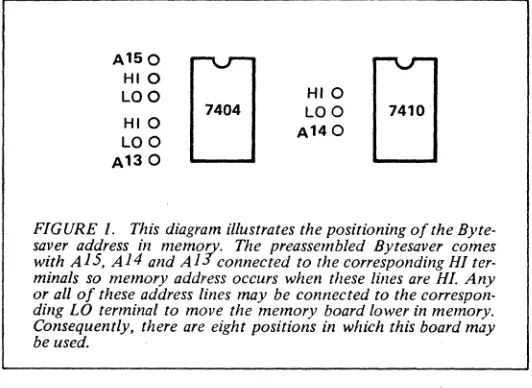
10. Install three jumper wires to select where the Bytesaver is to reside in memory. Each of the three high-order address lines (A15, A14 and A13) may be tied to either the corresponding "H" or "L" terminal. For example, in order for the Bytesaver to reside in the top BK of memory, the three jumpers should be in-stalled as shown below:
o
A15<0 HI OLO
o
HI A13<0 LO· 0
This adjustment causes the Bytesaver to reside in the top 8K of the memory map.
11. Install the ICs in their sockets, being careful to orient pin 1 of each IC as shown by the small white dot on the p.c. board at each IC position. Install a PROM containing the Bytemover software in PROM position zero.
Your Bytesaver is now fully assembled. Detailed operating in-structions are given in the Bytemover software section of this manual.
Notes
Interrupts: If you plan to have your computer respond to interrupts while executing a program stored in the Bytesaver memory, a small modification is required to the Bytesaver circuit. This modification is shown in Note 1 on the Bytesaver schematic.
BYTESAVER PARTS LIST
-
-
- - - -
- -
- -
- - - -
- - - -
- . --=...--:=
=======-=
====
~==---=
=-
-=-
;=-~=;=-~--=-Programming
PROMs
PROM programming with the Bytesaver is carried out by a sequence of memory write operations to the Bytesaver card. A sequence of approximately 100 memory write operations is required to write the data into each location of every PROM that you wish to program. This sequence of memory write oper-ations is carried out automatically when using the special instructions of Cromemco software. The Cromemco Z-80
Monitor, the Resident Operating System, and the 3K Control Basic Interpreter all have provision for PROM programming with the Bytesaver card. If your computer is equipped with front panel sense switches, our Bytemover software can be used for PROM programming. Operation of the Bytemover software is described in the next section.
B)'tesaver Parts List
Capacitors
C1-CS . . . • • . . . 0.1 uF C9-C15 . . . 10uF, 50V C16 . . . • . . . 005 C17 . . . 6S0 pF C1S . . • • • . • . • . . . • . . . • . . . 01 uF C19 . • . . . 6S0 pF C20 . . . • • • . • • • 150 pF C21-C23 . . . • • . . . • • . • . . . . • . . 0.1 uF
Diodes
01-019 . . . • . . . . 1 N914 or 1 N4531
Transistors
00-07 • • . • . . . • . . . . 2N3904
as,
09 • . . . • . . . . • . . . 2N3906 010 • . • . • . • . . . MPS6560 0", 012 . . • . . . 2N3904Resistors
R1 . • • . • . • . . . • . • • . . • • . . . • • 47K R2 . • . • • . . • . . . • 10K R3 . • • • • . . • . • . . . • • . . • . . 1S0 R4 . • • . • • . . . • . . . • . . . 1K R5 • • . . . • . . . • . . • . 9.1K R6 • • . . . • . . . • . . • . . . 1.5K R7 . . • . . . • . . . • • . . . • ,1.2K RS . • . . . • . . . . • . . . 47 R9 • • . . • . . . . • . . . • . . . 1K R10 . • • . '.' . • . • . . . • . . • . • . . . 10 R11 . • • . . . • • . . . • . . • . . . . 5.6K R12 • • • . . • . . . • . . • . . . . • • • . 5.6K R13 • . • • • • . . • • • . . . • . . . 10K R14 • . • • • • . • . • . . . • • . • . . . . 5.6K R15 • • • . . • . • • . • . . . • • . . . • • 1S0 R16-R31 • • • • • • • . • • • • • . • • • • • • 1SK .R32-39 • • • • • • • • • • • • • • • • • • • • • 4.7K
Integrated Circuits
IC1 . . • • . . . . • . . • . . . • . . . . • . 74123 IC2 • . . . • . • . . • • . . . • • . . . • . 7474 IC3 • • . . . • . • . . . • . • . . . 7402 IC4 . . • . • . • • • . • . • . . . . • . . • . • . 7406 IC5 . . • . . • • . . . • . . . • . . . • 7406 IC6 • • . • • • . • • • • . • • • . . . • • • . . 7402 IC7 . • • . • • . . . . • . • . . . • • . . . • 7406 ICS • . • • . • . • • • • . • • • . • . • . . . • 7442 IC9 • • • • . . • • . • • • . . . . • . • . . • 74L04 IC10 • • . . • . . . . • . • . . . • • • . . • 7410 IC11 • • • . • • . • • . . . • . • • . 74LS04 IC12* • . . . • . . . 340T-5.0 or 7S05 IC13* • . . . 320T-5.0 or 7905 IC14* • • . . • . . . • . 340T-12 or 7S12 IC15 • . . . • . . . 7432 or 74LS32 IC16 • • • . . . • . . . . • • • 74367 IC17 • • • . . • . . • . . . . • . . . . • • . 74367 IC1S • • • • • . . . • • . . . • . . • . • • . 74367 IC19 . . . • . . . • . . . . • . • • • . . 74367
Miscellaneous
SW1 . • . . • . . . p.c. board switch T1. . . XT8K pulse transformer
Sockets
10 . . . • . . . • . . . 14-pin 6 . • • . . . . • . . . • . . . • • . . 16-pin S . • . • • • . • . • . . • . . • • . . . • • . 24-pin
Hardware
3 • • . . . 6-32 by 3/S" screws . . • . • . . ; . . . 6-32 by 1/4" screw 1 ** ... 6-32 by 3/S" nylon screw 5 • . • • . • • • . . • • . . . • . . • • . 6-32 nuts 1 • . • • . • . . . • . . • • • • . Heatsink • . . • . • . • . . . • . . Insulating waSher
Notes
*The three voltage regulator ICs /lC12, IC13 & IC14) may look physically similar, however they are not interchangeable. Each must be in the proper IC location.
-BYTEMOVER SOFTWARE
is
:~_-- --:-~::- ~--...;.---== - - - - -
~- - -
~ ~Introduetion
Cromemco Bytemover software is designed to be used with the Cromemco 8K Bytesaver described. When you purchase a Bytesaver with one 2708 PROM, the Bytemover software is preprogrammed in that PROM.
The PROM containing the Bytemover software is normally inserted into PROM location zero on the Bytesaver board. The Bytemover software can be used to program a PROM in any of the PROM locations on the Bytesaver board. The Bytemover software can also be used to transfer programs from PROM to RAM.
The operation of the Bytemover software is controlled by setting front panel sense switches on any
S-'
00 bus·compatible computer. However, to use the Bytemover software there must be at least one RAM board in the computer beginning at loca· tion zero in the memory map. Furthermore, this RAM board must be unprotected for proper execution of the Bytemover software.Programming
Partiall~
Filled PROMs
Software can be loaded into a 2704 or 2708 in as small in-crements as you desire provided it is added to previously unused areas in that PROM.
This is done by first using Bytemover to move the current contents of the PROM down to RAM, adding the new software to an area of RAM which corresponds to the unused portion of the PROM and finally using Bytemover again to re-program the PROM with the new software.
Although the entire PROM must always be programmed, it never hurts to re-write the same information over again. And, of course, an erased PROM in which all bits are "1" may be pro· grammed at any time.
In general, it is OK to write a "1" over a "1", a
"a"
over a "0", or a ..a"
over a ",". But in order to write a "1" over a "0", the PROM must first be completely erased.If the PROM to which you want to add software is PROM zero on the Bytesaver board, turn off the A.C. power to"the computer and install a 1 N914 diode just below 00 (see step 3 of the Bytesaver assembly instructions).
Turn the power back on and move Bytemover down to RAM zero by following Example 1. Add the new software to an area of RAM which corresponds to an unused portion of PROM zero.
Re-program PROM zero by following Example 4 of this manual. Note that you need not erase the PROM to do this. Turn the computer power off and remove the 1 N914 diode below 00.
PROM Programming
Time
The Bytesaver software supplied here is designed to pro-gram a PROM in approximately 30 s.econds. We have found that this is generally a sufficiently long period of programming time. However-to be completely within the manufacturer's specifica-tions-the PROM should be programmed for 2 to 3 minutes.
If you wish to program your PROMs for longer than 30 sec-onds, the Bytemover software may be easily modified. Simply change the contents of location 77H from 40H to DOH. Now you must manually time the programming operation and de-press the stop switch at the end of the operation.
Step B)' Step Instructions
1. Before using the Bytesaver, you must install three jumper wires to set the location of Bytesaver in memory. This adjust-ment is shown in Figure 1. The assembled Bytesaver comes with A13, A14 and A15 each tied to the corresponding HI pad to position the board at the very top of memory. In the following instructions it is assumed this is the jumper connection used.
A150 HIO LOO HIO LOO
[image:5.612.313.579.194.388.2]A130
EJ
FIGURE 1. This diagram illustrates the positioning of the Byte-saver address in memory. The preassembled ByteByte-saver comes with A1S, A14 and A13 connected to the corresponding HI ter-minals so memory address occurs when these lilies are HI. Any or all of these address lines may be connected to the correspon-ding LO terminal to move the memory board lower in memory. Consequently, there are eight positions in which this board may be used.
2. Turn off all power to the computer and plug in the Byte-saver board.
3. Be sure the program power on the Bytesaver is turned off (program power switch in the down position).
4. Turn on the computer. Raise the reset switch, the stop switch and then raise the reset switch once again to initialize the computer.
5. Raise address switches A15, A14 and A13. All other ad-dress switches should be in the down position.
6. Raise the examine switch. You are now examining the con-tents of the first byte of PROM in PROM location zero of the Bytesaver memory board (memory location 340 000). If the PROM supplied with your Bytesaver is in this PROM location, the data lights will read "061,"the first byte of the Bytemover program.
Example 1: Transfer the Bytemover program from PROM to RAM beginning at location zero in RAM.
1. Raise the reset switch.
2. Depress the unprotect switch (on the Altair front panel). 3. Raise A 15, A 14 and A 13. Raise the examine switch. The data lights should read "061" octal.
4. Now set the sense switches for the task to be done, refering to Figure 2.
A15 Down to transfer from Prom to Ram. A14 Down for the transfer of 1 K bytes.
A13 Down All down since we are transferring from the
A12 Down
A 11 Down PROM that contains Bytemover (PROM 0).
Al0 Down
A9 Down All down for storage to begin at location
--
- -
-BYTEMOVEB SOFTWARE
~
==
=
===::;:::
===
S-=!=
==
- - -_____________________________ =
=
-=-
==:"~:;::or-=--=-A15 A14 A13 A12 A11 A10 A9 AS
0 0 0 0 0 0 0 0
UP
UP MSB LSB MSB LSB
To program a
For a 7K transfer.
PROM. PROM address location in
incre-Selection of RAM address in 1 K
DOWN DOWN ments of 1 K from the PROM in increments. To moveifrom
[image:6.612.313.579.447.537.2]For a 1 K transfer. which Bytemover is stored. PROM to RAM.
FIGURE 2: Function of the sense switches in Bytemover.
5. Push the run switch. In less than one second, the contents of PROM will be transfered to RAM. The contents of PROM are unaffected by this operation.
6. Raise the stop switch.
7. Raise the reset switch. Note that the data lights read "061".
Example 2: Program a 2708 PROM inserted in PROM location one. This PROM is to be programmed with the contents of the first 1 K bytes of RAM beginning at location zero in memory. The Bytesaver software is still in the PROM installed at PROM location zero on the Bytesaver board.
1. Raise the reset switch.
2. Depress the unprotect switch (on the Altair front panel). 3. Raise A15, A14 and A13. Raise the examine switch. The data lights should read "061" octal.
4. Raise the prote..:t switch on the Bytsaver board (i.e. program power switch to the on position). The protect light on the front panel should go off when this switch is raised.
5. Now set the sense switches for the task to be done:
A15 Up to program a PROM.
A14 Down (always down for PROM programming). A13 Down
To select the PROM 1 K higher in memory A12 Down
All Up than the PROM that contains Bytemover. Al0 Down All down for transfer to begin at location A9 Down
A8 Down zero in RAM.
6. Push the run switch. Note that panel light A9 is blinking at a rate of about twice per second. When this light stops blinking, the PROM programming is complete.
7. Raise the stop switch.
8. Now note the INTE light on the front panel. If this light is on, the Bytemover Verifier has verifed that the contents of the programmed PROM are indeed identical to the contents of the selected 1 K bytes of RAM. If this light is off, the PROM has not programmed correctly. This could be due to a defective PROM.
Example 3: Altair 8K BASIC can be stored in seven 2708 PROMs. Given that these seven PROMs are in PROM locations one through seven of the Bytesaver board, 8K BASIC can easily be transferred into RAM using the following procedure:
1. Raise the reset switch.
2. Depress the unprotect switch (on the Altair front panel). 3. Raise A15, A14 and A13. Raise the examine switch. The data lights should read "061" octal.
4. Now set the sense switches for the task to be done:
A15 Down to transfer from PROM to RAM. A14 Up for a 7K transfer.
A13 Down
To begin transfer from the PROM 1 K higher A12 Down
All Up in memory than the Bytemover program. Al0 Down
All down for storage to begin at location A9 Down
AS Down zero in RAM.
5. Push the run switch. In less than one second BASIC will be loaded into RAM (it sure beats paper tape!). Now raise the . stop-switch.
Example 4: If you do not have Bytemover in PROM, you can program a PROM with Bytemover that is stored in RAM. The Bytemover software (see listing) must first be loaded into RAM beginning at location zero in memory. The Bytemover software can then be burned into a PROM using the following procedure:
1. Raise the reset switch.
2. Depress the unprotect switch (on the Altair front panel). 3. Insert an erased PROM into PROM location zero. 4. Examine location 000 240 in memory.
5. Raise the program power switch on the Bytesaver board. 6.Set the sense switches with A 15. A 14 and A 13 up.
7. Push the run switch. When light A9 stops blinking, the pro-gramming is complete. The INTE light will be on.
.=---=.-. ... ...-... - - - - - - - -
-. BYTEMOVER SOFTWARE
§LS==S===~===~==
---==-
=- ---
=-:'=-=-:==-~~061 000 000
31~
000 000
151 333 377
056 000 172
371 041 013
172 346 004
000 151 174
170 376 374
346 004 007
371 041 000
333 377 107
351 306. 032
374 071 371
374 031 353
004 127 376
351 073 361
057 353 206
170 346 004
I
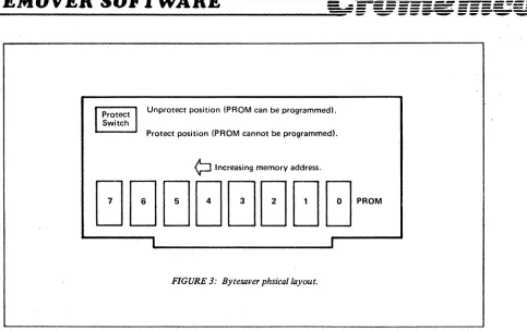
ProtectI
Unprotect position (PROM can be programmed). SwitchProtect position (PROM cannot be programmed).
¢:llncreasing memory address.
[image:7.612.76.559.39.343.2]I I
FIGURE 3: Bytesaver phsicai layout.
Erasing PROMS: The 2704 and 2708 PROMs are erased by shining intense U.V. light through their quartz windows. One such U.V. source is available for $125 from Prometrics, 5345 North Kedzie Av., Chicago, IL 60625.
B~temover
].1
Octal Listing
301 321 056 311 363
34~ 34~000 000 000
061 002 000 341 061 004 000 325 305 371
127 346 007 007 007 107 172 346 070 017
3~3
346 200 017 017 306
O~~041 000 000
000 071 353 371 353 021 000 000 073 361
007 007 000 205 157 351 000 000 076 126
140 371 147 056 153 001 000 000 073 361
077 037 037 346 100 056 175 205 157 351
007 007 205 157 351 000 000 000 174 041
374 031 353 147 056 153 170 346 370 306
346 340 036 000 113 127 170 346 037 107
157 333 377 346 100 017 017 205 157 351
056 315 147 351 000 000 000 000 373 351
056
361 147 001 000 000 351 000 326 220
070 077 076 000 037 205 157 351 000 000
353 276 353 027 346 001 057 074 205 157
353 306 007 077 027 346 001 057 074 205
057 074 205 157 351 000 000 000 000 000
-BYTEMOVER ASSEMBLY LISTING
~--
-
--:::-~---
:"
=
---::=
=- --- ;=-==-=-
:==-~-=-0000
0000
0000
0000
0000
0000
0000
0000
0000 31 00 00
0003
0003 Cl
0004 01
0005
0005 2E C9
0007 F3
0008 E5
0009 E5
OOOA 00
OOOB 00
OOOC 00
0000 31 04 00
0010 CD 00 00
0013
0013 31 02 00
0016 El
0017
0017 31 04 00
OOlA 05
OOlB C5
001C
001C F9
0010 OE 00
001F 59
0020 69
0021
0021 DB
FF
0023 57
0024
0024 E6 07
0026 07
0027 07
0028
0028
47---0029 7A
002A
002A E6 38
002C OF
0020 00
002E 67
002F 39
0030 2E 00
0032 7A
0033 EB
0034
0034
0000
*
BYTEMOVER <T.M.) SOFTWARE FOR
0001
*
CROMEMCO 8K BYTESAVER <T.M.)
0002
*
VERSION 3. 1
0003
*
SELF-RELOCATING SOFTWARE LOCATABLE AT ANY
0004
*
1024 BYTE (lK) BOUNDARY IN MEMORY
0009
*
ROUTINE TO FIND ONESELF IN MEMORY
0010 SP EGU 6
0019
*
DEFINE FIRST 4 BYTES IN MEMORY AS STACK
0020
LXI SP, 0
0029
*
SAVE FIRST FOUR BYTES IN REGISTERS
0030
POP B
0040
POP 0
0049
*
REPLACE BYTE 0 WITH A 'RETURN'
0050
MVI L. OC9H
0051
DI
0060
PUSH H
0070
PUSH H
0080
NOP
0081
NOP
0082
NOP
0090
LXI SP, 4
0100
CALL 0
0101
*
ROM LOCATION NOW IN BYTE 3
0110 LXI SP, 2
0120 POP H
0129
*
RETURN BYTES 0-3
0130 LXI SP,4
0140
PUSH D
0150 PUSH B
0159
*
STORE ROM LOCATION IN SP
0160 SPHL
0170 MVI
C,
0
0180 MOV E,C
0190
MOV
L.
C
0199
*
INPUT SENSE SW COMMANDS
0200
IN 255
0210 MOV D,A
0219
*
STRIP RAM ADDRESS
0220 ANI 7
0230 RLC
0240 RLC
0249
*
STORE RAM ADDRESS IN BC
0250 --
·~OVB, A
0260 MOV A,D
0269
*
ST~IPROM ADDRESS
0270
ANI 56
0280
RRC
0290
NOP
0300
MOV H,A
0310
DAD SP
0320 MVI L,
0-0330
MOV A,D
0340
XCHG
BYTEMOVERASSEMBLY LISTING
~--
-
----~--:
=
---.-;::==
=- --- =-=-
==--=-
=-:::
==--=--=-0034 E6 80
0036
OF
0037 OF
0038 C6 2D
003A 21 00 00
003D 6F
003E 39
003F E9
0040
0040 F9
0041 21 OB 00
0044 39
0045 EB
0046 F9
0047 EB
0048 11 00 00
004B
004B
004B 3B
004C
004C Fl
004D 02
004E
004E 03
004F
004F 13.
0050 7A
0051 E6 04
0053 07
0054 07
0055 00
0056 85
0057 6F
0058 E9
0059 00
005A 00
005B
005B 3E 56
005D 85
005E 6F
005F E9
0060
0060 00
0061
0061 69
0062 7C
0063 60
0064
0064 F9
0065 67
0066 2E 6B
0068
0068 01 00 00
006B
006B 3B
006C
0350
0360
0370
0380
0390
0400
0410
0420
0500
0510
0520
0530
0550
0560
0570
0580
0588
0589
0590
0599
0600
0610
0619
0620
0629
0630
0640
0650
0660
0670
0680
0690
0700
0710
0716
0717
0719
0720
0725
0730
0740
1000
101'0
1019
1020
1030
1040
1049
1050
1060
1070
1079
1080
1089
1090
1098
ANI
128
RRC
RRC
ADI
45
LXI H, 0
MOV
L,A
DAD
SP
PCHL
*
ROUTINE TO TRANSFER ROM TO RAM
SPHL
LXI
H, 11
DAD SP
XCHG
SPHL
STACK CONTAINS ROM LOCATION
XCHG
H&L CONTAIN LOOP ADDRESS
LXI
D, 0
*
START OF TRANSFER LOOP
*
INCREMENT ROM ADDRESS
DCX SP
*
MOVE DATA FROM ROM TO RAM
POP
6
STAX B
*
INCREMENT RAM ADDRESS
INX B
*
INCREMENT BYTE COUNT
INX
D
MOV A,D
ANI
4
RLC
RLC
NOP
ADD L
MOV L,A
PCHL
NOP
NOP
*
~UMPTO
OOBI
FROM TRANSFER ROUTINE
MVI A,
56H
ADD L
MOV L.A
PCHL
*
ROUTINE TO PROGRAM ROM
NOP
*
MOVE RAM ADDRESS INTO HL
MOV
L,C
MOV A,H
MOV H,B
*
MOVE RAM ADDRESS INTO SP
SPHL
MOV H.A
MVI L,
107
*
INCREMENT RAM ADDRESS
LXI
8, 0
*
INCREMENT RAM ADDRESS
DCX SP
-
---
-
--- -
-BYTEMOVER ASSEMBLY LISTING
=--==-===a=--_
===~
.=
---==-;:: ---;:
=---=-- ==-
;"~-=-006C
006C F1
006D
12
006E
006E 13
006F
006F 03
0070
0070
0070 78
0071
0071 FE FC
0073 3F
0074 1F
0075 1F
0076
0076 E6 40
0078
0078 2E 7D
007A 85
007B 6F
007C E9
007D 2E 6B
007F 78
0080 E6 04
0082
0082 07
0083 07
0084 07
0085 85
0086 6F
0087
0087
0087
0087
0087 E9
0088 00
0089 00
008A 00
008B
008B
008B 7C
008C 21 00 FC
008F
008F 39
0090 F9
0091 21 00 FC
0094
0094 19
0095 EB
0096 67
0097 2E 6B
0099 78
009AE6 F8
009C
009C C6 08
1099
1100
1110
1119
1120
1129
1130
1138
1139
1140
1149
1150
1160
1170
1180
1198
1200
1201
1205
1210
1220
1225
1226
1230
1240
1241
1250
1260
1270
1280
1290
1291
1292
1293
1294
1300
1350
1360
1370
1378
1379
1380
1390
1399
1400
1410
1420
1429
1430
1440
1450
1460
1470
1480
1489
1490
*
TO MOVE DATA FROM ROM TO RAM
POP 6
STAX D
*
INCREMENT ROM ADDRESS
INX
D
*
INCREMENT BYTE COUNT
INX B
*
B STORES TWO CONSTANTS
*
#
COMPLETE PASSES
&
IN ROM CNT
MOV A,B
*
#
PASSES
=
32
?
CPI 252
CMC
RAR
RAR
*
SET 64 TO 0 FOR TWO MINUTE TIMER
ANI 64
*
A=64 IF COMPLETED 32 PASSES
MVI L, 7DH
ADD L
MOV L,A
PCHL
MVI
L,
6BH
MOV A,B
ANI 4
*
A=4 IF END OF 1024 BYTE PASS
RLC
RLC
RLC
ADD L
MOV L,A
*
GO BACK TO 1090 UNLESS OVERFLOW
*
THEN GO TO 1380 FOR
*
ADDRESS SUBTRACTION
*
OR 2135 FOR QUITS
PCHL
NOP
NOP
NOP
*
ANOTHER PROGRAM PASS TO BE DONE
*
ADJUST ROM AND RAM ADDRESSES
MOV A,H
LXI H, 64512
*
SUBTRACT 1024 FROM ROM ADDRESS
DAD SP
SPHL
LXI
H,
64512
*
SUBTRACT 1024 FROM
RAM
ADDRESS
DAD D
XCHG
MOV H,A
MVI L, 107
MOV A,B
ANI 248
*
INCREMENT PASS CONTER BY ONE
ADI 8
BYTEMOVER ASSEMBL Y LISTING
==
~::.:.-
=...::...=. __
=..::..=.
.::E:_ -:.=--=
==
==
=
=
==:;:
=
=
a=-===
---= - - - ---- -...,. ... ""'-""'"
~009E 47
009F
009F E9
OOAO
OOAO DB FF
00A2 47
00A3 E6 EO
00A5 lE 00
00A7 4B
00A8 57
00A9 78
OOAA E6 1F
OOAC 47
OOAD 67
OOAE 2E 60
0080 E9
0081
0081 C6 lA
0083 6F
0084 DB FF
0086 E6 40
0088 OF
0089 OF
008A 85
008B 6F
OOBC E9
0080
0080
0080 7C
OOBE 21 00 FC
00C1 39
00C2 F9
00C3 2E CD
00C567
00C6 E9
00C7 00
00C8 00
OOC9 00
OOCA 00
OOCB
OOCB FB
OOCC E9
OOCD
OOCD
OOCD 7C
OOCE 21 00 FC
0001 19
0002 EB
0003 2E Fl
0005 67
0006 01 00 00
0009 E9
OODA 00
OODB
0008 06 90
0000 6F
1495
1499
1500
2000
2010
2020
2030
2040
2050
2060
2070
2080
2090
2100
2110
2120
2121
2122
2123
2124
2125
2126
2127
2128
2129
2130
2133
2134
2135
2145
2155
2165
2175
2185
2195
2205
2210
2215
2220
2229
2230
2240
2248
2249
2250
2260
2270
2280
2290
2300
2310
2320
2625
2629
2630
2640
MOV 8,A
*
GO BACK TO 1090
PCHL
*
ROUTINE TO LOAD BYEMOVER INTO ROM
IN 255
MOV B,A
ANI 224
MVI E, 0
MOV C,E
MOV D,A
MOV A,B
ANI 31
MOV B,A
MOV H,A
MVI
L
96
PCHL
*
CHECK FOR 7K TRANSFER OF ROM TO RAM
ADI lAH
MOV L,A
IN 255
ANI 64
RRC
RRC
ADD L
MOV L,A
PCHL
*
PROGRAMMER VERIFICATION ROUTINE
*
PART 1
MOV A,H
LXI H, 64512
DAD SP
SPHL
MVI
L.
OCDH
MOV H,A
PCHL
NOP
NOP
NOP
NOP
*
ROM TO RAM TRANSFER STOP ROUTINE
El
PCHL
*
PROGRAMMER VERIFICATION ROUTINE
*
PART 2
MOV A,H
LXI H,64512
DAD 0
XCHG
. MVI L, OF1H
MOV H,A
LXI B, 0
PCHL
NOP
*
7K TRANSFER COMPLETION CHECK
SUI 90H
BYTEMOVER ASSEMBLY LISTING
== -
-=-=
---
===--
-=--=::~~~ =55-~·~==-=
==
-=.---
===~.:::::
-OODE 7A
2650
MOV A,D
OODF C6 04
2660
ADI 4
OOEl 57
2670
MOV D,A
00E2 FE
38
2680
CPI 56
00E4 3F
2685
CMC
00E5 3E 00
2690
MVI A, 0
00E7 IF
2700
RAR
00E8 85
2710
ADD L
00E9 6F
2720
MOV
L.
A
OOEA E9
2730
PCHL
OOEB
2879
*
ROM PROGRAMMER STOP ROUTINE
OOEB 00
2880
NOP
OOEC 00
2881
NOP
OOED FB
2885
EI
OOEE E9
2890
PCHL
OOEF E9
2900
PCHL
OOFO E9
2906
PCHL
OOFl
2918
*
PROGRAMMER VERIFICATION ROUTINE
OOFl
2919
*
PART 3
OOFl 3B
2920
DCX SP
00F2 Fl
2930
POP 6
00F3 EB
2940
XCHG
00F4
2949
*
COMPARE FOR GREATER
00F4 BE
2950
CMP M
00F5 EB
2960
XCHG
00F6 17
2970
RAL
00F7 E6 01
3000
ANI 1
00F9 2F
3010
CMA
OOFA 3C
3011
INR
AOOFB 85
3015
ADD L
OOFC 6F
3020
MOV L.A
OOFD 3B
3030
DCX SP
OOFE 3B
3040
DCX SP
OOFF
3050
*
COMPARE FOR LESSER
OOFF Fl
3055 POP 6
0100 2F
3056
CMA
0101 EB
3058
XCHG
0102 86
3059 ADD M
0103 EB
3060
XCHG
0104 C6 07
3061
ADI A,
1
0106 3F
3065
CMC
0107 17
3070 RAL
0108 E6
a1
3090 ANI
1
010A 2F
3100
CMA
010a 3C
3101
INR A
OlOC 85
3105 ADD L
OlOD 6F
3110 MOV L,A
OlOE 03
3130
INX a
OlOF 13
3140
INX D
0110 78
3150 MOV A,B
0111 E6 04
3180
ANI 4
0113 2F
3190 .CMA
0114 3C
3191
INR A
0115 85
3195
ADD L
0116 6F
3200 MOV L.A
2708-Z704 PROM DATA
-
~~~...---- - - -
-=.. ---...:.-=-.=-==
=======.
====":5..:
---_
...
:::;;;;;:::-
-
-
-
-
-..-.--
...
---
---
----PIN CONFIGURATIONS
A, 24 Vec
A. AS
AS
A. Va.
A.
27081 CSIWE
A2 2704 lobo
A, PR0GRAM
AO O.
0, 9 0,
0, o.
03 11 Os
I.!;s 0,
'2704 = Vss 2708= Ag
C s I W E
-Ag-Ag
ADDRESS INPUTS
PIN NAMES
ADDRESS INPUTS DATA OUTPUTS
CHIP SELECT !WRITE ENABLE INPUT
BLOCK DIAGRAM
CHIP SELECT LOGIC
Y
DECODER
·
·
·
,
X
·
DECODER
·
,READ OPERATION
DATA OUTPUT
0,-0.
I
OUTPUT BUFFERS
Y GATING
64 X 128 ROM ARRAY
--DC t:I Operating Characteristics
TA =
ooc
to 70°C, Vee=
+5V ±5%, Voo=
+12V ±5%, Vee = -5V ±5%. Vss = OV. Unless Otherwise Noted_Symbol Parameter Min. Typ)1) Max. Unit Conditions
ILl Address and Chip Select Input Load Current 10 p.A VIN
=
5.25V-ILO Output Leakage Current 10 p.A VOUT
=
5.25V. CS/WE = 5V too Voo Supply Current 50 65 mA Worst Case Supply Currents:IcC Vee Supply Current 6 10 mA All Inputs High
lee
Vee Supply Current 30 45 mA CSIWE = 5V; TA '" O°C VIL Input Low Voltage Vss 0.65 VVIH Input High Voltage 3.0 Vee+ 1 V
VOL Output Low Voltage 0.45 V IOl = 1.6mA VO H1 Output J:1igh Voltage 3.7 V tOH = -100p.A VOH2- Output High Voltage 2.4 V IOH
=
-1mA Po Power Dissipation 800 mW TA=
70°CNOTES: 1. Typical values are for T A = 25° e and nominal supply voltages.
2. The program input (Pin 18) may be tied to VSS or Vec during the read mode.
---
--
-
----
---2708-2704 PROM DATA
==--=
=
=-=
=
=
===
==
=
==-===
---..:== - - - - -..-.. - -- ...
~...--Waveforms
(Logic levels and timing reference levels same as in the Read Mode unless noted otherwise.)
Program Mode
CS/WE = +12V
+ - - - O N E PROGRAM L O O P - - - . I
ADDRESS
26V
PROGRAM PULSE
O V - - - J ]
ADDRESS 0
Read/Program/Read Transitions
ry
· · ·
X
ADDRESS 1023r
~/\---J
, , - - - - , } L
ADDRESS 1
~~~
_l,..>---PR~~~pAM---\
ADDRESS
---~/I~---12V
CSIWE 5V
26V
PROGRAM PULSE
/
v
o--+---~
DATA
0,-08
DATA OUT
VALID DATA IN VALID
DATA IN
-iii : - - - -
-:- - - _
-:---..;= - - - - ...
2708-2704 PROM DATA
~... -
~ ~AC Charaeteristies
TA =O°C to 70°C, VCC = +5V ±5%, VOO = +12V ±5%, VBB = -5V ±5%, VSS = OV, Unless Otherwise Noted.
Symbol Parameter Min. Typ. Max. Unit
tACC Address to Output Delay 280 450 ns
tco Chip Select to Output Delay 120 ns
tOF Chip De-Select to Output Float 0 120 ns
toH
Address to Output Hold 0 nsCapacitance!
1 ] TA = 25°C, f=
1 MHzSymbol Parameter Typ. Max. Unit Conditions
CtN Input Capacitance 4 6 pF VIN=OV
COUT Output Capacitance 8 12 pF VOUT=OV
Waveforms
Note 1. This parameter is periodically sampled and not 100% tested.ADDRESS
--x---'1X~----C.s.IWE
DATA OUT
OUTPUT SINK CURRENT
vs.
OUTPUT VOLTAGET~pieal
Charaeteristies
(Nominal supply voltages unless otherwise noted):
ACCESS TIME VS.LOAO CAPACITANCE
RANGE OF SUPPL Y CURRENTS VS. TEMPERATURE
400
J
T .. -25"C
8 0 , - - - , - - - - , - - - , - - - , - - - - ,
ALL POSSIBLE OPERATING CONDITIONS:
---
r--~
---
;....-300
i
g
200~<
100
100 200 300 400
c;, (pF)
60
<C
.!
en
~ Z
w a:
40 a:
::>
<J
>
-'
A.
Q,
::>
en
20
SOO 20 40 60
Vee =5.25V
Voo ·12.6V Vee = -S.2SV
i
so
'DO I
2708-2704 PROM DATA
!
"
"
1·:<
ACCESS TIME VS. TEMPERATURE
500
1 TTL
lOAD
"'1~F
400
300
-""
~
~
MAXIMUM JUNCTION TEMPERATURE VS. AMBIENT TEMPERATURE
150 , - - - . , - - - , . . - - - , . . - - - . ,
200
--
--100
o
-20 o 20
50 ---~---+_---+_-~
40 60 80 o~----~----~---~~ o 20 ~ 60 ~
PROGRAMMING OPERATION
Description
Initially, and after each erasure, a" bits of the 2708/2704 are in the "1" state (Output High). Information is introduced by select-ively programming "0" into the desired bit locations.
The circuit is set up for programming operation by raising the CS/WE input (Pin 20) to +12V. The word address is selected in the same manner as in the read mode. Data to be programmed are presented, 8-bits in parallel, to the data output lines (0,-08). Logic levels for address and data lines and the supply voltages are the same as for the read mode. After address and data set up one program pulse (Vp) per address is applied to the program input (Pin 18). One pass through a" addresses to be programmed is defined as a program loop. The number of loops (N) required is a function of the program pulse width (tpw) according
to-N x tpw ~ 100 ms.
For program verification, program loops may be alternated as shown on page 12.
Program Characteristics
TA
=
25°C, Vcc=
+5V ±5%, VDD=
+12V ±5%, Vss=
-5V ±5%, Vss=
OV, CS/WE=
+12V, Unless Otherwise Noted.Symbol Parameter Min. Typ. Max. Units
tAS Address Setup Time 10 J.ls
tess CS/WE Setup Time 10 J.ls
tos Data Setup Time 10 J.ls
tAH Address Hold Time 1 J.ls
tCH CS/WE Hold Time .5 J.ls
tOH Data Hold Time 1 J.ls
tOF Chip Deselect to Output Float Delay 0 120 ns
tOPR Program To Read Delay 10 J.ls
tpw Program Pulse Width .1 1.0 ms
tpR Program Pulse Rise Time
.5
2.0 J.lstpF Program Pulse Fall Time
.5
2.0 J.lsIp Programming Current 10 20 mA
Warrant~
Your factory-built Bytesaver is warranted against defects in materials and workmanship for a period of 90 days from the date of delivery. We will repair or replace products that prove to be defective during the warranty period provided that they are returned to Cromemco. No other warranty is expressed or implied. We are not liable for consequential damages.
Should your factory-built Bytesaver fail after the warranty period it will be repaired, provided that it is returned to Cromemco, for a fixed service fee. We reserve the right to refuse to repair any product that in our opinion has been subject to abnormal electrical or mechanical abuse. The service fee is currently $35 and is subject to change.
f'-~-r--t---r---r----r--~(··V)
••
...
".
,
.
L--£~-'---1---~--1r--r--~M~~~:n)
-,
•. 'Il
RT
,.
..
I.'"
0
IT
I
C "":' 10".' ':'
t---I-r---Ircs----oo+lzv
T~~f
iC>'''-••
3 •••
..
'0 79
, 8O
••
.
,
••
31••
3<J..
~••
8
•
'7 te."
...
00 T 90 14
II! •
..
DO • 40 I '9 15 ~
00
.~
to00
.~
~
Inll
':'1'2111018715"321'.1
ROM 7 IS t4 15 II 1718 192021222324
AA~
1.l..' .. · ..
J
ROil.
IS 14 1& 18''7 '.,920.11222324
A!~
§11---I~c-i. ~1--II~c-
.. --It-c,---O-••
llO~F
.b
10,.-
JOO,.-Inl
.
1
1"""" .. "
ROIl.
IS M 15 lEi 17,. ,,20 21222324
J.
-~ ~
-1'1.., .. · ..
1110114 .'.1
IS 14 151& 17 Ie I. 20ZI R223M
.+.
!
l:L
--
-~L
.. ,. , .. "
...
ta'4 'S It 17 181'20 2122252
rL ...
J
110M •
.a 14 IS ,e: 1718 19 20 21222524
.+.
!
~
-
J.
!~
COPYRIGHT 1975 BY CROMEMCO BOARD REV. 2
SCHEMATIC REV. 2
NOTE:
I. DASHED MODIFICATION FOR ROM RESIDENT INTERRUPT OPERATION (NOT INCLUDED ON STANDARD CARD) 2. ALL DIODES ARE IDENTICAL (lN914 OR EQUIV.)
~ill
=1"1I109a7854321.1
ROil' IS fit " 16 17 18 19 20 2\ 22 2324
J.
!~
r~L
... "
RO"OIS 141516 1718192021222324
A!~
·S
,.
2 17 5 45 I:M",
~-§)D"
~~DI'
rt-B
D
"
rt~DI'
rtr~OI'
-::- I
I
I
00
.~
~r_--+++_~----+-+_---+++_~----+-+_---++1_-4----+_1_---~~~----+_1_---~~~----~~---4HH-~----H-~---~~ .. ~----~~---~~~----~~---~~
,.
I
r-s
OII14 16 la
I
,.
DO
.~
DO
'~
DD.~
A '2 . .
•
A II I" IS •
..
A 10 lIT
'
.
tnP'
n
I
I I7_ .
5 4 • • 7 ' ":"'.. ., . . . 11 •
!
*
L..
~
U.. ID Q...
~,
..
".
,..
0.--.,
•
10• 4
•
...
•
...
Er"·
••
..
-~?'
AIS~'
.---":"":";050 •
...
~,
',/Q
It.~.
..
-'"
J..
..
~ ~
I .. O.0 -
...
".
""
-....
,..
I
_""--
.. 13 4...
....
.
..-- ""-J
•
,
••
•
•
,....
•
""
".
18K..
••
'"
..
~
15 2 ~...
....
18'
:-...
...
•
,
•
It•
....
II. +S"r-+-
+S I 747.4·- I'·' I
~
.
...
10'••
..
,
..
-
..
...
~
5 l ' Q,.83904
,
,
..
'='
~~.
lA....
,
..
• S
I
(27V PEAk)
~
t 7 Z 00..
...,.
=
I
-71r--;"
13 3 7..
"
~
--sO!~ I
L-..
Rit
e.6K
...
.~904
.
""""
"
,
.
7 13Ria ...
,
..
'0.
:-•
....
...
•
•
.5O~
.:
~--I '5 I 45 SOUT
,
!-:,~,E-,+---I.e ." •