ISSN Online: 2162-5328 ISSN Print: 2162-531X
DOI: 10.4236/ampc.2019.97010 Jul. 31, 2019 123 Advances in Materials Physics and Chemistry
Impact Thickness on Structural and Electrical
Characterization of Nickel Phthalocyanine
Thin Films
Eman M. Nasir
1, Mohammed T. Hussein
1, Addnan H. Al-Aarajiy
21Department of Physics, College of Science, University of Baghdad, Baghdad, Iraq 2Department of Physics, College of Science, University of Babylon, Babylon, Iraq
Abstract
Thin films of Nickel Phthalocyanine have been prepared by evaporation technique for (50 - 350 nm) of thickness. XRD studies show that the thin films have single crystalline structure for low thicknesses with (100) orienta-tion and the crystallite size increased with increased thickness. Also from the AFM technique for NiPc films, the roughness wasdetermined and the grain size increases with increasing of thickness from except at thickness 350 nm. The studies of electrical properties, morphology and orientations of the crys-tallites are important to understand and predict the nature of the films and essential for their successful applications in solar cell and sensors. The elec-trical properties of these films were studied with different thickness, NiPc has three activation energy. Carrier’s concentration and mobility was calculated. Hall measurements showed that all the films are p-type.
Keywords
Nickel Phthalocyanine, Vacuum Evaporation, XRD, AFM, Morphology, Thin Film, Electrical Properties
1. Introduction
Nowadays, semiconducting organic materials are very important since they have successful application in optical and electronic devices. One of these materials is Phthalocyanines (Pcs); it has significant properties which made it a good alter-native for development electronic devices. These materials have been used in the gas sensor and in electronic devices because it possesses many advantageous properties such as thermal, chemical and photochemical stability, excellent film How to cite this paper: Nasir, E.M.,
Hus-sein, M.T. and Al-Aarajiy, A.H. (2019) Im-pact Thickness on Structural and Electrical Characterization of Nickel Phthalocyanine Thin Films. Advances in Materials Physics and Chemistry, 9, 123-132.
https://doi.org/10.4236/ampc.2019.97010
Received: March 31, 2019 Accepted: July 28, 2019 Published: July 31, 2019
Copyright © 2019 by author(s) and Scientific Research Publishing Inc. This work is licensed under the Creative Commons Attribution International License (CC BY 4.0).
DOI: 10.4236/ampc.2019.97010 124 Advances in Materials Physics and Chemistry growth and good optical and electronic properties [1]. Their thermally stable nature makes them suitable for thin film deposition by thermal sublimation. These materials have also shown promise for photoconductive and photovoltaic response [2]. Phthalocyanines are a class of planar aromatic organic compounds that have attracted a great deal of attention for quite some time because of their unique properties such assemiconductivity, photoconductivity, photochemical reactivity, chemical stability, electrochromism, bio-organic and catalytic activity and their application in the field of colour display technology and gas sensors. The electrical, optical and structural properties of phthalocyanine thin films de-pend on different parameters such as evaporation rate, substrate temperature and post-deposition annealing [3][4]. In addition to their excellent photocon-ductive properties, Pc-s have the advantages of being very stable against thermal and chemical decomposition and present very intenseoptical absorption in the visible region. These properties similarity to chlorophyll have many applications in solar cell. Also, they have the potential to serve as active material for molecu-lar electronic devices such as electrochromic displays, chemical sensors and opt-ical data storage. Furthermore, interests in Pc compounds have recently been renewed due to the discovery that they form molecular metals after partial oxi-dation [5]. The physical properties of thin films materials depend very much on the structure properties; therefore, they have always high priority. The know-ledge of the composition of the film is important to understand and predict the nature of the films [6]. Thin films of Phthalocyanines are chemically and ther-mally durable and are prepared by vacuum thermal evaporation [7][8][9]. NiPc is thermally stable and its thin film can be deposited by thermal evaporation without dissociation [10][11]. A number of analytic techniques are available for the composition characterization of thin films. These include X-ray diffraction studies, AFM and electrical studies. The objective of this paper is to study the ef-fect of thickness on the structural, compositional and electrical studies of Nickel phthalocyanine (NiPc) thin films prepared by vacuum evaporation technique.
2. Experimental
Nickel phthalocyanine thin films, with thickness (50, 110, 265 and 350) nm, were deposited on cleaned glass substrate (type corning, China) with dimensions (7.5 × 2.5 × 0.1) cm by thermal evaporation technique (Edwaed coating unit model 306 A) under high vacuum with pressure of (6 × 10⁻⁵) mbar with deposition rate
of about 20 nm/min. A molybdenum boat was used as a source for the evapora-tion of the material. Set a distance of 15cm to separate the substrate and the boats. The films were characterized by X-ray diffraction technique using (Philips X-ray diffractometer) with CuK α radiation at wavelength (1.5406) A˚. Atomic force microscopy was used to determine the roughness snd surface morphology of films. Digital electrometer type Keithly 616 and electrical oven have been used for electrical measurements. The Hall coefficient (RH), carrier type and Hall
DOI: 10.4236/ampc.2019.97010 125 Advances in Materials Physics and Chemistry 40) V and two digital electrometers (Keithley type 616 to measure the current and voltage
3. Results and Discussion
3.1. X-Ray Diffraction XRD
X-ray diffraction pattern of NiPc thin film with different thickness (50, 110, 265 and 350) nm are shown in Figure 1 respectively. XRD pattern indicates that all the samples are single crystal and that it has β-crystalline phase [12]. The differ-ence between α- and β-phases is attributed to the tilt angle of b-axis of the unit cell. The structure of the NiPc thin film is determined as tetragonal with prefe-rential orientation along the (100) direction. Well-defined diffraction peaks by (100) give the direction of the preferential orientation as deposited film (JCPDS, file No. 11-0744). The diffraction peaks are agreement with the previous obser-vations [1]-[10]. The spacing between the planes (d) has been calculated using the Bragg’s formula:
2 sind
θ
=nλ
(1) as shown in Table 1. The d values obtained from diffractogram are in agreement with JCPDS record. The differences in the d values are attributed to higher X-ray absorption, sample purity, particle size, preferred orientation and crystal texture [13][14]. Table 1 shows the structure parameters of NiPc films, The full width at half maximum (FWHM) intensity of preferential orientation, shows that the FWHM are reduced with increasing thickness except at thickness 350 nm its in-creased, which means re arrangement the lattice structure and fill all dangling bind and eliminate the defect [12][15][16] and then its increased due to create a localized state at 350 nm. From the Table 1 it is observed that the grain size in-creases which intern dein-creases strain and dislocation density. The grain size D of the film is calculated using the Scherrer relationcos
D k= λ β θ (2) where k = 0.94 is a constant,
λ
—the wavelength of x-ray, β—the full width half maximum and θ—the diffraction angle, the grain size increases from (20.85 - 33.5 nm) for thickness (50 - 265 nm) and then decreased to 23.2 at 350 nm as in Figure 2, and this may be attributed to enhancement and re-crystallization these films by increasing the thickness. And the decreasing in grain size at 350 may be attributed to create a localized state by increasing thickness. The intensities of other planes have disappeared. The XRD spectra also shows a little shifting to-wards lower diffraction angle for (100) plane normally which means greater spacement between atoms which according to Brag equation. The sample which has thickness 265 nm is the lowest FWHM which means the greatest grain size according to Scherrer equation.DOI: 10.4236/ampc.2019.97010 126 Advances in Materials Physics and Chemistry Figure 1. X-ray diffraction of the NiPc thin films with deferent thicknesses.
Figure 2. Grain size with thickness of NiPc thin films.
Table 1. X-ray diffraction parameters of the NiPc thin films with deferent thicknesses.
Thickness nm (degree) 2θ (A˚) d FWHM Grain size (nm) ε * 10−3 δ * 10−5 Line/nm2
50 6.9654 12.6804 0.3986 20.85 1.735 2.298
110 7.0218 12.5787 0.3735 22.2 1.625 2.018
265 7.0068 12.6056 0.2479 33.5 1.079 0.889
350 6.9751 12.66282 0.3583 23.2 1.559 1.857
0 50 100 150 200 250
5 15 25 35
2θ (deg)
I (
cp
s)
50 nm
0 50 100 150 200 250
5 15 2θ (deg)25 35
In
te
ns
ity
(c
/s
)
110 nm
0 250 500 750 1000 1250 1500 1750
5 15 25 35
2θ (deg)
I (
cp
s)
265 nm
0 50 100 150 200 250
5 15 25 35
2θ (deg)
I (
cp
s)
[image:4.595.208.538.622.732.2]DOI: 10.4236/ampc.2019.97010 127 Advances in Materials Physics and Chemistry 2
n D
δ = (3)
where n is a factor, when equal unity giving minimum dislocation density. The microstrain is related to the lattice misfit, which in order depends on the deposi-tion condideposi-tions. The microstrain ε is calculated using the relation [17]:
cos 4
ε β= θ (4)
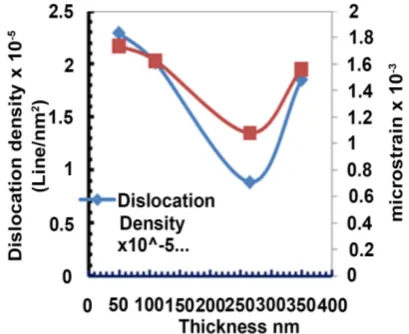
Figure 2 and Figure 3 represent the grain size and dislocation density δ and the microstrain ε of prepared thin films evaporated with different thicknesses on glass substrates. It was observed that the dislocation density and microstrain ex-hibit a decreasing trend with the deposition thin film thickness (except at 350 nm) which represents better lattice quality.
3.2. Surface Morphology
Atomic Force Microscope
This section of studies includes the effect of thickness on the morphology of prepared films were determined by Atomic Force Microscope with different thickness (50, 110, 265 and 350) nm taken in an area of 10 × 10 μm2 as shown in
[image:5.595.271.476.535.702.2]Figure 4. It is observed from the figure that the morphology of these films was uniform surface with clear grain boundaries and growth of crystal and the grain size increases from 48.33 - 203.28 nm with increasing thickness from 50 - 265 nm except at thickness 350 nm its decreased to 91.25 nm as in Figure 4 and Ta-ble 2, and it's decreased at 350 nm and this is agreement with the results of XRD. Also the typical topography of a polycrystal is observed, where each grain can be clearly individualized. Differences in the height of the grains can also be ob-served, as well as a visible dispersion of the grain size. It is observed that at 350 of thickness, the grains are somewhat smoothed out. The roughness (rms) of films at different thickness is given in Table 2. It is observed that the roughness increase with thickness increase, and this is agreement with other researchers [18][19][20].
DOI: 10.4236/ampc.2019.97010 128 Advances in Materials Physics and Chemistry Figure 4. 3-D AFM images of NiPc thin films with different thicknesses.
Table 2. Grain size and average roughness of NiPc thin films by AFM technique.
Thickness (nm) Roughness Average (nm) Grain Size (nm)
50 5.29 48.33
110 6.2 87.17
265 6.31 203.28
350 8.97 91.25
Electrical properties
The electrical conductivity of NiPc thin films was performed to determine the thermal activation energy. Measurements were carried out in the temperature range 303 to 473 K for films with different thickness ranging from 50 to 350 nm. The temperature dependence of the conductivity can be expressed by Arrhenius equation. [11]:
(
)
exp E k TB
σ σ= ∆ (5)
where ΔE is the thermal activation energy and kB is the Boltazmann’s constant.
[image:6.595.208.539.419.505.2]DOI: 10.4236/ampc.2019.97010 129 Advances in Materials Physics and Chemistry Figure 5. Lnσ as a function of (1000/T) of NiPc thin films for different thicknesses.
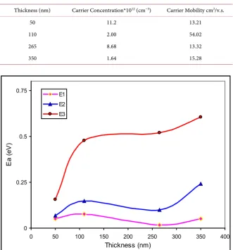
figure, there are three semiconductor distinct linear parts, which correspond to three activation energies ΔE1, ΔE2 and ΔE3. ΔE1 corresponds to extrinsic region
and represents transition process for carriers within localized states in the energy gap and this suggests the existence of high density of localized states in the energy gap, and ΔE2 and ΔE3 corresponds to intrinsic region and represents the
carriers transport across the grain boundaries by thermal excitation. The change in the slope and hence the activation energy is interpreted as a change from ex-trinsic to inex-trinsic conduction [21]. The value of the thermal activation energy ΔE1, ΔE2 and ΔE3 is shown in Table 3, which is in good agreement with those
obtained by other workers [22] [23]. The room temperature conductivity in-creases as the thickness inin-creases and this is attributed to the change in the de-gree of crystallinity. Also, as given in Figure 6, the activation energyvaries as the thickness increases and this is because of the improved crystallinity with the in-crease of the grain size.
3.3. Hall Effect
Carrier concentration and Hall mobility have been determined from Hall mea-surements for NiPc thin films, having different thicknesses which were depo-sited on glass substrates at 300 K. The Carrier concentration (n) is determined for all film thicknesses and it is of p-type. Hall coefficient (RH) was calculated,
then carrier concentration has been calculated for each thickness and it was of p-type. Carrier mobility was determined for each thickness. All these parameters are shown in Table 4. It can be inferred from the Table that carrier mobility creases with the decrease of the carrier concentration and varies with the in-crease of film thickness. This is consistent with the work of researchers [23]. -15.5
-15 -14.5 -14 -13.5 -13 -12.5 -12
2 2.2 2.4 2.6 2.8 3 3.2 3.4
1000/T (K-1)
Ln
(σ
)
DOI: 10.4236/ampc.2019.97010 130 Advances in Materials Physics and Chemistry Table 3. Values of activation energies and conductivity for NiPc thin films with different thicknesses.
Thickness nm
σR.T × 10−7
(Ω∙cm)−1 ΔE1 (eV) Temp∙Range(K) ΔE2 (eV) Temp∙Range(K) (eV) ΔE3 Temp∙Range(K) 50 18.524 0.051 307 - 333 0.0691 338 - 389 0.156 400 - 454
110 6.476 0.076 333 - 369 0.147 373 - 413 0.477 413 - 446
265 8.654 0.017 305 - 348 0.099 348 - 403 0.518 403 - 458
[image:8.595.207.539.233.589.2]350 4.948 0.051 307 - 353 0.241 363 - 403 0.603 418 - 473
Table 4. Values of carrier concentration and carrier mobility for NiPc thin films with different thicknesses.
Thickness (nm) Carrier Concentration*1012 (cm−3) Carrier Mobility cm2/v.s.
50 11.2 13.21
110 2.00 54.02
265 8.68 13.32
350 1.64 15.28
Figure 6. Effect of NiPc thin films thickness on activation energy.
4. Conclusions
Thin films of Ni-Pc were prepared by the thermal evaporation method on glass substrates with different thickness successfully. From the x-ray diffraction stu-dies, it is observed that the structure is single crystalline β-phase film-oriented preferentially (100) plane for all thickness. The structure properties are found to be very sensitive to the thickness of thin film. The grain size increases with
in-0 0.25 0.5 0.75
0 50 100 150 200 250 300 350 400
Thickness (nm)
E
a
(eV
)
DOI: 10.4236/ampc.2019.97010 131 Advances in Materials Physics and Chemistry creasing thickness. The change in grain size shows that the properties of NiPc are controlled by its structure and morphology depending on increases the thickness. The surface morphology of prepared films and the crystal morphology vary with thickness. From the electrical properties measurements, there are three semiconductor distinct linear parts, which correspond to three activation ener-gies ΔE1, ΔE2 and ΔE3. ΔE1 corresponds to extrinsic region and ΔE2 and ΔE3
correspond to intrinsic region. Hall effect measurements show that all the films are p-type. The carrier mobility increases with the decrease of the carrier con-centration and varies with the increase of film thickness.
Conflicts of Interest
The authors declare no conflicts of interest regarding the publication of this pa-per.
References
[1] Petraki, F., Papaefthimiou, V. and Kennou, S. (2005) A Study of the Ni-Phthalocyanine/Gold Interface Using X-Ray and Ultraviolet Photoelectron Spectroscopies. Journal of Physics: Conference Series, 10, 135-138.
https://doi.org/10.1088/1742-6596/10/1/033
[2] Newton, M.I., Starke, T.K.H., Willis, M.R. and McHale, G. (2000) NO Detection at Room Temperature with Copper Phthalocyanine Thin Film Devices. Sensors and Actuators B, 67, 307-311. https://doi.org/10.1016/S0925-4005(00)00542-6
[3] Narayanan Unni, K.N. and Menon, C.S. (2000) Electrical, Optical and Structural Studies on Nickel Phthalocyanine Thin Films. Materials Letters, 45, 326-330. https://doi.org/10.1016/S0167-577X(00)00127-0
[4] Kumar, G.A. (2002) Optical Studies of Phthalocyanine Molecules in PMMA Matrix. Materials Letters, 55, 364-369. https://doi.org/10.1016/S0167-577X(02)00394-4
[5] Kumar, G.A., Jose, G., Thomas, V., Unnikrishnan, N.V. and Nampoori, V.P.N. (2003) NIR to UV Absorption Spectra and the Optical Constants of Phthalocya-nines in Glassy Medium. Spectrochimica Acta Part A: Molecular and Biomolecular Spectroscopy, 59, 1-11. https://doi.org/10.1016/S1386-1425(02)00037-9
[6] Kalugasalam, P. and Ganesan, S. (2010) Compositional Analysis of Annealed Lead Phthalocyanine Thin Films. International Journal of Engineering Science and Technology, 2, 2574-2579.
[7] El-Nahass, M.M., Atta, A.A., El-Sayed, H.E.A. and El-Zaidia, E.F.M. (2010) Elec-trical Transport Mechanisms and Photovoltaic Characterisation of MgPc/p-Silicon Hybrid Organic-Inorganic Solar Cells. Current Organic Chemistry, 14, 84-88. https://doi.org/10.2174/138527210790226447
[8] Hussein, M.T., Eman, M.N. and Senaed, F.A. (2014) Optical Properties of Cobalt Phthalocyanine Thin Films. Indian Journal of Research, 3, 145-147.
[9] Hussein, M.T., Nasir, E.M. and Al-Aarajiy, A.H. (2012) Study on the UV-Visible of Ni-Phthalocyanine Thin Film Optical Properties. International Journal of Thin Films Science and Technology, 1, 71-76.
[10] Fiodorov, M.I. (1999) Gas Sensor. Russia Patent 2124719.
DOI: 10.4236/ampc.2019.97010 132 Advances in Materials Physics and Chemistry Physics and Chemistry, 3, 113-119. https://doi.org/10.4236/ampc.2013.31A014
[12] Joseph, B. and Menon, C.S. (2007) Studies on the Optical Properties and Surface Morphology of Nickel Phthalocyanine Thin Films. E-Journal of Chemistry, 4, 255-264. https://doi.org/10.1155/2007/643834
[13] Kalugasalama, P. and Ganesanb, S. (2010) Surface Morphology of Annealed Lead Phthalocyanine Thin Films. International Journal of Engineering Science and Technology, 2, 1773-1779.
[14] Shihub, S. and Gould, R. (1993) Structure and Phase-Change Phenomena in Eva-porated Thin Films of Cobalt Phthalocyanine. Physica Status Solidi (A), 139, 129-138. https://doi.org/10.1002/pssa.2211390110
[15] Ji, Z.G., Wong, K.W., Tse, P.K., Kwok, R.W.M. and Lau, W.M. (2002) Copper Phthalocyanine Film Grown by Vacuum Deposition under Magnetic Field. Thin Solid Films, 402, 79-82. https://doi.org/10.1016/S0040-6090(01)01702-3
[16] Kalugasalam, P. and Ganesan, S. (2010) Structural Analysis of Annealed Lead Phthalocyanine Thin Films. International Journal of Engineering Science and Technology, 2, 2567-2573.
[17] Gopal, S., Viswanathan, C., Karunagaran, B., Narayandass, S.K., Mangalaraj, D. and Yi, J. (2005) Preparation and Characterization of Electrodeposited Indium Selenide Thin Films. Crystal Research and Technology, 40, 557-562.
https://doi.org/10.1002/crat.200410383
[18] Aziza, F., Sulaimana, K., Muhammad, M.R., Sayyad, M.H. and Karimov, K. (2011) Influence of Thermal Annealing on the Structural Properties of Vanadyl Phthalo-cyanine Thin Films: A Comparative Study. International Journal of Materials and Metallurgical Engineering, 5, 693-695.
[19] Larramendi, E.M., Calzadilla, O., Gonzalez-Arias, A., Hernandez, E. and Ruiz-Garcia, J. (2001) Effect of Surface Structure on Photosensitivity in Chemically Deposited PbS Thin Films. Thin Solid Films, 389, 301-306.
https://doi.org/10.1016/S0040-6090(01)00815-X
[20] Neghabi, M., Zadsar, M. and Ghorashi, S.M.B. (2014) Investigation of Structural and Optoelectronic Properties of Annealed Nickel Phthalocyanine Thin Films. Ma-terials Science in Semiconductor Processing, 17, 13-20.
https://doi.org/10.1016/j.mssp.2013.08.002
[21] Locklin, J. and Bao, Z. (2006) Effect of Morphology on Organic Thin Film Transis-tor Sensors. Analytical and Bioanalytical Chemistry, 384, 336-342.
https://doi.org/10.1007/s00216-005-0137-z
[22] Soliman, H.S., El-Barry, A.M.A., Khosifan, N.M. and El Nahass, M.M. (2007) Structural and Electrical Properties of Thermally Evaporated Cobalt Phthalocyanine (CoPc) Thin Films. The European Physical Journal Applied Physics, 37, 1-9. https://doi.org/10.1051/epjap:2006135