1
Faculty of Electrical Engineering,
Mathematics & Computer Science
SLOW WIRELESS
COMMUNICATION TESTBED
BASED ON SOFTWARE-DEFINED RADIO
Zhiyuan Wang
Master Thesis
26 November 2017
I would first like to express my special thanks to all of my supervisors, Dr. Andre Kokkeler,Dr. Arjan
Mei-jerink, Siavash Safapourhajari and Zaher Mahfouz. Thanks for your sincere assistance and valuable guidance during my whole master project. Thanks for Siavash Safapourhajari. Your office was always open when I ran into trouble or had a problem in my project. Your careful review and modification on my thesis helps me a lot in improving my thesis. Thanks for Zaher Mahfouz who provides me support in experimental devices.
I would also like to thank my friends, Matheus Terrivel and Konstantino Fatseas. Thanks for your compan-ion and encouragement during my master project.
Finally, I must express my profound gratitude to my father Bin Wang and to my aunt and uncle Jian Zhang & Hao Lu for providing me with constant supports and continuous encouragements throughout my years of study in the Netherlands and through the process of my final project. This thesis would not have been possible without them. Thank you again.
Zhiyuan Wang
November 21, 2017
Enschede
The Netherlands
SUMMARY
The Internet of Things (IoT) extends the virtual cyber world into the real physical world by networking everyday smart physical objects, representing an upgraded version of Internet. The wireless sensor networks (WSN) are playing diverse sensing functions for IoT and feeding information from the physical world to the virtual cyber world. Nowadays, most of the WSNs are deployed to detect slow-changing physical quantities and data from every sensor node in these WSNs varies very slowly over a long time interval. Accordingly, a low data transmission rate is sufficient for the sensor nodes. Moreover, the low data rate makes it possible to apply very narrowband (VNB) radio communication with a bandwidth of a few kHz in wireless sensor nodes. It is noteworthy that most of wireless sensor nodes are transmitting data in the unlicensed 2.4GHz frequency band where the dominant interference is characterized by relatively wide bandwidth. Therefore, if a very narrowband (VNB) radio is adopted in a wireless sensor node, only a small portion of co-channel wideband interference will overlap with the VNB signal transmitted by the wireless sensor node. Because only a small portion of the wideband interferer’s power is superimposed onto the VNB signal, the VNB signal captured by a receiver has a relatively high signal-to-noise ratio (SNR). Therefore, it is possible to reduce the power of the transmitter or release the noise of the receiver.
Power consumption is a key factor that determines the lifetime of a sensor node because most of sensor nodes are powered by batteries. Once a battery is depleted, the lifetime of a sensor node will expire. The radio transceiver on a wireless sensor node consumes a lot of power when it is working. However, the VNB radio communication makes it possible for the radio transceiver to decrease its transmission power while guaranteeing the same bit error ratio (BER). Thus, the low power consumption is made possible by the VNB radio transceiver.
In this research project, the VNB radio transceiver is called “slow wireless radio”. It aims at the wireless sensor nodes that transmit data at very-low instantaneous bit-rates (100∼1000bps) in the 2.4GHz frequency
band full of wideband interference while achieving low power consumption. The goal of this project is to build up a point-to-point VNB radio communication testbed based on software-defined radio (SDR). This testbed will serve as a design reference to investigate the feasibility of the VNB radio communication when it is used in wireless sensor nodes and facilitate the development of a slow-wireless sensor node prototype.
The VNB radio communication testbed is composed of a VNB transmitter and a VNB receiver where binary phase shift keying (BPSK) is used as modulation format and double differential encoding/decoding helps the testbed eliminate the effects of frequency and phase offsets. The bit transmission rate can be adjusted by repeater at the transmitter side while the accuracy of received bits is improved by DC-offset compensation and timing recovery at the receiver side.
The testbed can conduct the real-time measurements of signal-to-noise ratio (SNR) and bit error ratio (BER). The experimental results indicate that successful VNB wireless communication can be implemented on the testbed.
List of Acronyms vi
1 INTRODUCTION 1
1.1 Research Background . . . 1
1.2 Research Motivation. . . 1
1.3 Works of Others . . . 2
1.4 Slow Wireless Radio. . . 3
1.5 Research Problem Description . . . 4
1.5.1 Research Scope . . . 4
1.5.2 Research Goals . . . 5
1.6 Thesis Outline . . . 5
2 EXPERIMENT PLATFORM 6 2.1 Software-defined Radio . . . 6
2.2 SDR Development Kit . . . 7
2.2.1 GNU Radio . . . 7
2.2.2 Survey on other SDR development tools . . . 8
2.2.3 Why is GNU radio chosen? . . . 9
2.3 SDR Platform . . . 10
2.3.1 What is SDR platform? . . . 10
2.3.2 Survey on SDR platforms . . . 11
2.3.3 Why is bladeRF chosen? . . . 12
2.3.4 bladeRF Introduction . . . 13
2.3.5 bladeRF Internal Structure . . . 14
2.4 LMS6002D Transceiver . . . 15
2.4.1 Introduction. . . 15
2.4.2 Internal Structure . . . 16
3 TRANSMITTER DESIGN 18 3.1 Transmitter Structure Overview . . . 18
3.2 BPSK Modulator . . . 19
3.3 Double Differential Encoder Design . . . 20
3.4 Repeater . . . 21
3.5 IQ Modulator . . . 23
4 RECEIVER DESIGN 27 4.1 Receiver Structure Overview . . . 27
4.2 IQ Demodulator . . . 28
4.2.1 IQ Demodulation . . . 28
4.2.2 IQ Imbalance . . . 31
4.3 DC Offset Compensation . . . 32
4.4 Double Differential Decoder Design . . . 33
CONTENTS v
4.5 Matched Filter and Sampler Design . . . 35
4.5.1 Repeater and Integrator . . . 36
4.5.2 Matched Filter. . . 37
4.5.3 Sampler . . . 39
5 TESTBED DESIGN AND EXPERIMENT 41 5.1 Testbed Design. . . 41
5.1.1 GNU Radio Data Types. . . 42
5.1.2 Sample Rate vs. Symbol Rate . . . 43
5.1.3 Transmitter Implementation . . . 44
5.1.4 Receiver Implementation. . . 45
5.1.5 Channel Model for Software Simulation . . . 46
5.1.6 RF Interface for Hardware Experiment . . . 47
5.2 SNR and BER . . . 47
5.2.1 SNR and Eb/No . . . 47
5.2.2 BER vs. Eb/No. . . 48
5.2.3 SNR Estimator . . . 48
5.2.4 BER Calculator . . . 50
5.2.5 Cross Correlator . . . 51
5.3 BER Performance . . . 52
5.3.1 Software Simulation for BER versus Eb/No. . . 53
5.3.2 Software Simulation for BER versus Phase Offset . . . 54
5.3.3 Software Simulation for BER versus Frequency Offset . . . 55
5.3.4 bladeRF Test. . . 56
6 CONCLUSION 60 6.1 Conclusions . . . 60
6.2 Recommendations . . . 60
Bibliography 62
Appendices
A IQ MODULATION AND DEMODULATION 66
AWGN additive white gaussian noise
ADC analog-to-digital converter
BER bit error ratio
BPSK binary phase shift keying
bps bits per second
DC direct current
DAC digital-to-analog converter
DSP digital signal processor
FPRF field programmable radio frequency
FPGA field programmable gate array
FIR finite-impulse response
HDL hardware description language
IF intermediate frequency
IC integrated circuit
ISM Industrial, Scientific and Medical
IoT Internet of Things
IADC in-phase analog-to-digital converter
IDAC in-phase digital-to-analog converter
IQ in-phase and quadrature
LE logic elements
LNA low-noise amplifier
LO local oscillator
LSB least significant bit
LPF low-pass filter
MAC medium access control
M2M4 second and fourth order moment
NRZ non-return-to-zero
CONTENTS vii
PLL phase-locked loop
PSK phase shift keying
PA power amplifier
QPSK quadrature phase shift keying
QADC quadrature analog-to-digital converter
QDAC quadrature digital-to-analog converter
RF radio frequency
RRC root-raised cosine
RX receive
SNR signal-to-noise ratio
SDR software-defined radio
SMA subminiature version A
SoC systems-on-chip
SPI serial peripheral interface
SWIG simplified wrapper and interface generator
TX transmit
USRP universal software radio peripheral
UWB ultra-wideband
VNB very narrowband
VGA variable-gain amplifier
WSN wireless sensor network
CHAPTER
1
INTRODUCTION
This chapter will start with a background introduction on the research. Then, it will state the motivation behind the research and reviews the works that have been done in this research field. Section1.4will propose the concept of slow wireless radio. The concrete research problems in this project will be formulated in section1.5. This chapter will be concluded by the outline of the thesis.
1.1
Research Background
Wireless communication is defined as the transmission of information over a distance between two or more terminals without relying on any form of electrical conductors such as cables and wires. The wireless trans-fer of information is usually achieved by various types of electromagnetic waves (such as radio waves, mi-crowaves and infrared light). Radio waves (with electromagnetic wave frequency between 3kHz to 300GHz) are the most common information carrier in most of wireless communication technologies. With radio waves, the wireless communication distance can span from a few meters to thousands of kilometers [1], [2]. In modern society, wireless communication technology is ubiquitous and applied in a wide range of portable electronic devices such as mobile phone, GPS receiver, laptop computer and so on.
The Internet of Things (IoT) refers to the inter-networking of a wide variety of smart physical objects. It represents an upgraded version of Internet which extends from virtual cyber world into real physical world by interconnecting everyday physical objects. With the help ofIoTtechnology, the physical objects in the real world are no longer disconnected from the virtual world but can communicate with the virtual world on the Internet anytime and anywhere. Every smart object is equipped with microprocessor, sensor, actuator, communication and networking modules. It is able to collect, process and exchange data. TheIoTmakes ubiquitous computing possible and has great application potentials to revolutionize the future society. It is expected that more than 30 billionIoT-based smart objects will be connected to the Internet by 2020 [3], [4]. Because it is impractical to interconnect a tremendous number of smart objects via wires, theIoTis completely based on the wireless communication technology.
The wireless sensor network (WSN) refers to the network formed by a large number of spatially distributed wireless sensor nodes. Equipped with sensor, microprocessor, wireless transceiver module and power module, each node can detect, process and transfer various physical quantities such as temperature, humidity, pressure, etc. The WSN is one of the most pivotal constituent parts in the IoT, playing diverse sensing roles for IoT and feeding information from the physical world to the virtual cyber world [5]. Hence, WSN has become a hot research topic in academia and industry.
1.2
Research Motivation
Nowadays, most ofWSNs are applied in monitoring environmental conditions such as temperature, humidity and pressure or structural conditions such as buildings and bridges. The data that is collected by each sensor node in a monitoring WSN typically varies very slowly over the time. The data packet that is transmitted by
CHAPTER 1. INTRODUCTION 2
each sensor node every time contains simply a very small amount of available information. That is to say, each sensor node only needs to transfer a small amount of data over a long time interval. Therefore, it is sufficient for wireless sensor nodes in monitoring applications to transfer data at very-low bit rate.
Meanwhile, the wireless transceiver modules which are embedded in most of wireless sensor nodes are working in 2.4 GHz Industrial, Scientific and Medical (ISM) band because the ISM band is an unlicensed radio frequency band. However, due to this advantage, the spectrum resources in this band are overused by other radio signals such as Wi-Fi and Bluetooth. As a result, strong radio interference is posing a major challenge for the wireless sensor nodes working in the ISM band [6].
Besides strong radio interference, a major challenge for wireless sensor nodes is power consumption. The amazing progress in integrated circuit (IC) manufacturing technology in last decades makes it possible to integrate sensor, microprocessor and transceiver within a tiny systems-on-chip (SoC). However, there has not been much progress in miniaturizing batteries with high-volume power density. The small structure of a wireless sensor node severely constrains the size of a battery that can be fitted on the sensor node. Ultra-thin button cell is the typical battery whose size fits for the wireless sensor node. In most of applications a large number of wireless sensor nodes are deployed in all kinds of harsh environments such that it is impossible to replace the battery for every sensor node. Hence, the lifetime of a sensor node is determined, to a large extent, by the lifetime of its battery. Once the battery is depleted, the lifetime of the sensor node will expire. In order to prolong the lifetime of a sensor node as much as possible (up to several years), the technologies achieving ultra-low power consumption are highly preferred in designing wireless sensor nodes. Otherwise, widespread deployment of wireless sensor nodes would still be infeasible in many applications.
In practice, the radio transceiver module consumes a large portion of energy in a sensor node [7]. Thus, it is absolutely necessary to design an energy-efficient radio transceiver with satisfying robustness to strong co-channel interference for the wireless sensor nodes working in monitoring applications.
1.3
Works of Others
Some solutions have been proposed to achieve low power consumption in radio transceiver modules used for wireless sensor nodes. These solutions are duty-cycling radio, wake-up radio and ultra-wideband (UWB) radio. Each solution has its own weaknesses and limitations.
The sensor node with duty-cycling radio [8]–[10] turns on its radio module in short bursts of time for data transmission and turns it off most of the time to conserve energy. Since the moments when data transmissions happen are uncertain, the duty-cycling radio needs very accurate timing but it is rather difficult to achieve accurate timings in aWSNformed by hundreds of sensor nodes.
The wake-up radio [11]–[13] enables a sensor node to consume very little power when listening the radio channel of interest and wake up its main radio module for data reception when the desired signal is detected. However, the wake-up radio is prone to co-channel interference. If the interference that exists in the channel of interest is strong and persistent, the wake-up radio would frequently activate its main radio module by mistake.
TheUWBradio [14]–[16] transmits data by generating pulse trains in specific time intervals while occu-pying a wide bandwidth. Because of the ultra-wide bandwidth of the UWB radio, it demonstrates its good coexistence with narrowband radios in the same channel. However, due to radio emission regulations [17], it is restricted to short transmission range of a few meters. Moreover, its power consumption is relatively high compared with other low power radio schemes.
1.4
Slow Wireless Radio
The slow wireless radio is a wireless communication scheme which is capable of transferring data at in-stantaneous bit-rates as low as 100 bits per second (bps) in interference-intensiveISMband while achieving ultra-low power consumption.
Due to the fact that the majority of wireless sensor nodes are applied in detecting slow-varying physical quantities, the data traffic produced by a single sensor node is extremely low. Thus, it is doable for a sensor node to transmit data at a low bit rate. The low bit rate makes it possible to utilize very narrowband (VNB) radio communication in the order of a few kHz.
Furthermore, most of wireless sensor nodes are transmitting and receiving signal in the unlicensed 2.4 GHz ISMfrequency band, which is overused by diverse radio signals such as Wi-Fi and Bluetooth. However, it is noteworthy that the dominant radio interference (like Wi-Fi) within the ISM band is spreading over wide bandwidth with relatively low power spectral density. This is because spread spectrum techniques are widely adopted in wireless communication technologies such as Wi-Fi and Bluetooth.
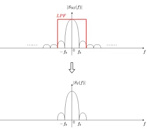
As a result, when aVNBsignal with high power spectral density coexists with the wideband interferer with low power spectral density in the ISM band, only a small portion of the interferer overlaps with the VNB signal as illustrated in Fig.1.1. In brief, the wideband interferer within the ISM band has limited impact on the VNB signal.
Figure 1.1:Wideband interference impact on very narrowband (VNB) signal
Therefore, the receiver can still capture the VNB signal with acceptable signal-to-noise ratio (SNR) in pres-ence of interferpres-ence. Moreover, due to higherSNRof the received VNB signal, it is also possible to reduce the transmission power at the transmitter side or relax the noise figure requirement at the receiver side while guaranteeing acceptable bit error ratio (BER) [18].
In a word, theVNBsignal enables the slow wireless radio to have reduced transmission power while guar-anteeing acceptable BER so that it is possible to achieve low power consumption on the slow wireless radio. To summarize, the slow wireless radio is aiming at the wireless sensor node that is transmitting data:
1. at very-low instantaneous bit-rate of 100∼1000 bps
2. in interference-intensive ISM frequency band
3. with ultra-low power consumption
CHAPTER 1. INTRODUCTION 4
1.5
Research Problem Description
1.5.1
Research Scope
From the perspective ofWSN, there are primarily four functional layers [19], [20] in its hierarchical model as shown in Fig.1.2:
Figure 1.2:The hierarchical model of a wireless sensor network
• The application layer is responsible for formatting data and managing data flow in an optimal scheme for specific applications.
• The network layer is responsible for assigning addresses for nodes and routing data through the net-work.
• The medium access control (MAC) layer provides error-free transfer of data frames from one node to another over the physical layer. It is also responsible for data stream multiplexing, data frame detection, channel access control and error control.
• The physical layer transmits and receives radio signals over physical medium between any two nodes. This layer is also responsible for carrier frequency selection and generation, radio channel access, signal detection, conversion between bits and radio signals, modulation/demodulation, encoding/decoding, etc.
[image:11.595.255.369.180.338.2]The hardware structure of a wireless sensor node that is illustrated in Fig.1.3generally includes four parts: a sensor, a microcontroller, a wireless transceiver and a power management module. The research scope is focused on the physical layer in aWSNor the wireless transceiver in a wireless sensor node.
1.5.2
Research Goals
In this research project, aVNBwireless communication testbed will be built up based on software-defined radio (SDR) for the purpose of simulating a real point-to-point VNB wireless communication link and mea-suring its relevant communication performance. ThisVNBcommunication testbed will assist researchers to investigate the feasibility of the VNB communication when it is applied in wireless sensor nodes. Further-more, this testbed can also serve as a slow-wireless-radio reference design to facilitate the development of a wireless sensor node prototype that is based on the slow wireless radio.
The objectives in this research project are formulated as follows:
1. AVNBtransmitter and aVNBreceiver will be modeled in software.
2. Successful communication through a channel model between theVNBtransmitter and theVNBreceiver will be simulated in software.
3. A real-world point-to-point wireless communication testbed that integrates theVNBtransmitter and theVNBreceiver will be implemented on anSDRplatform.
4. Real-time measurements onBERandSNRare conducted in software when theVNBcommunication link is running on theSDRplatform.
In this research project, GNU radio is chosen asSDRdevelopment kit and bladeRF asSDRplatform.
1.6
Thesis Outline
CHAPTER
2
EXPERIMENT PLATFORM
This chapter will start with an introduction to software-defined radio. Then, it will discuss the details with regard toSDRdevelopment toolkit (GNU radio) andSDRplatform (bladeRF) that are used in building up the VNBcommunication testbed in this research project. Finally, this chapter will conclude with the discussion of LMS6002D transceiver, which is a core component in bladeRFSDRplatform.
2.1
Software-defined Radio
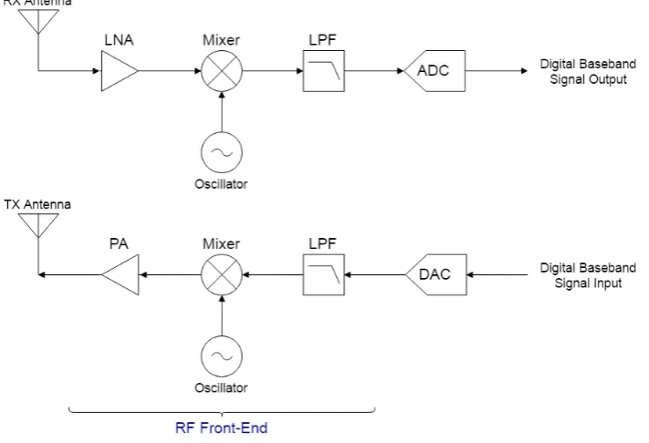
A radio communication system is a system which can communicate information via electromagnetic waves in radio frequency (RF) spectrum from 3kHz to 300GHz. A typical radio communication system is composed of a transmitter and a receiver. The transmitter modifies signal for efficient radio transmission and typically contains: modulator, encoder, digital-to-analog converter (DAC), filter, gain amplifier, mixer and power am-plifier (PA). The receiver captures theRFsignal and reconstructs the original signal. Typical components in the receiver are low-noise amplifier (LNA), mixer, gain amplifier, filter, analog-to-digital converter (ADC), demodulator and decoder.
Traditionally, all of the components in a radio communication system used to be implemented mostly by a variety of dedicated electronic circuits. As the processing capability of digital processors evolves rapidly, lots of signal processing tasks which used to be done by dedicated electronic circuits are now carried out by general-purpose high-performance digital processors instead. As a result, an emerging radio technology called software-defined radio (SDR) relies on signal processing software running on a personal computer or a general-purpose processor to implement as many components as possible in a radio communication system. The exact definition of the software-defined radio is as follows:
“Software-defined radio (SDR) is a radio communication system where some components that have been typ-ically implemented in hardware (e.g. amplifiers, filters, modulators/demodulators, encoders/decoders, etc.) are instead implemented by means of software on a personal computer or embedded system[22].”
The block diagram for a typical SDR transceiver system is depicted in Fig.2.1. It consists of:
• An SDR platform (such as bladeRF SDR).
• An SDR development kit and SDR software (such as GNU radio).
• A personal computer.
Figure 2.1:SDR transceiver system block diagram [23]
AnSDRplatform includesRFfront-end andADC/DAC. It serves as a bridge between analog RF signal and digital baseband signal, performing tasks such as mixing and analog-to-digital or digital-to-analog conversion which are impossible to be implemented by software.
Unlike the conventional radio system in which digital baseband processing is performed by dedicated circuit or specialized digital signal processor (DSP), anSDRsystem processes all of the digital baseband signals by means of SDR software which is running on a general-purpose computer. Relying on SDR development kit which is installed on the computer, user can easily configure SDR platform and develop SDR software for digital baseband signal processing.
The most significant advantages of theSDRsystem are reconfigurability, reusability and flexibility. The SDR platform can be easily reconfigured to work in varying frequencies, bandwidths, sample rate and so on. The SDR software can be easily developed and modified for a variety of digital baseband processing and the same software codes can be reused in different communication systems. Due to these features, the SDR system is considerably flexible in implementing diverse radio communication systems using the same hardware.
2.2
SDR Development Kit
TheSDRdevelopment kit is a software development platform where all digital signal processing algorithms used in software-defined radio can be developed in flowgraph or coding. In this section, GNU radio is intro-duced in detail and some other popular SDR development tools are also investigated briefly.
2.2.1
GNU Radio
GNU radio is a free-of-charge and open-source software development toolkit for developing various signal processing algorithms used in radio systems. GNU radio features a rich variety of signal processing blocks, which enable user to easily develop and implement diverseSDRapplications. Many signal processing blocks which can be found in conventional radio systems can also be found in the library of GNU radio such as filters, modulators/demodulators, coders/decoders and so on [24]. GNU radio development toolkit can be either used together with many kinds of SDR platforms to build up real-world radio communication systems or used alone without any SDR platform to simulate radio communication systems only by software [25].
CHAPTER 2. EXPERIMENT PLATFORM 8
written in C++ codes. However, the flow graphs in GNU Radio Companion are compiled and run in Python scripts. In case that some special signal processing blocks are missing in the library or unsatisfying users’ requirements, users are able to quickly create their own signal processing blocks in Python. In GNU radio, C++ is basically used for low-level signal processing blocks whose computational performance is critical while Python is used for high-level flow graph which serves as a framework to control the data flows among different blocks.
In order to make sure that all of the C++ signal processing blocks are accessible from the Python flow graph, simplified wrapper and interface generator (SWIG) is used in GNU radio. TheSWIGis a software interface compiler that connects programs written in C/C++ with a variety of high-level scripting languages such as Python. It works by parsing the interface of a C/C++ program and then generating the glue code for the target scripting language so that the scripting language can call or access the C/C++ program via the glue code [26]. Figure2.2reveals the GNU radio framework structure where theSWIGis used as an interface between the signal processing blocks written in C++ codes and the flow graph implemented by Python scripts. In order to communicate with SDR platform, GNU radio has some specialized SDR interface blocks which connect the GNU radio flow graph running on a computer with an SDR platform. The commonly-used SDR interface block is osmocom block, which supports most of available SDR platforms.
Figure 2.2:GNU radio framework structure [27]
2.2.2
Survey on other SDR development tools
In this section, we briefly investigate other twoSDRdevelopment tools: MATLAB Simulink and NI LabVIEW.
• MATLAB Simulink
MATLAB Simulink developed by MathWorks is a graphical programming and development environment for modeling, simulating, analyzing, testing and verifying model-based dynamic systems. User can easily build up a dynamic system by drawing flowgraph. Algorithms written in MATLAB codes can be incorporated into modules in the flowgraph and simulation results from model-based system in flowgraph can be exported into MATLAB for further analysis.
supported SDR platforms can directly exchange data with communication system models in the MATLAB Simulink. The parameters for these SDR platforms can also be configured in the MATLAB Simulink [28], [29].
• NI LabVIEW
The laboratory virtual instrument engineering workbench (LabVIEW) developed by National Instrument (NI) is a system design and development environment. Its intuitive graphical programming method enables user to design system model in visual flowgraph.
The LabVIEW communication system design suite provides all necessary functional blocks used for build-ing communication system models. C/C++ and MATLAB codes can also be embedded into functional blocks in LabVIEW flowgraph. The LabVIEW communication system design suite supports some popular SDR plat-forms such as Ettus SDR platplat-forms and NI SDR platplat-forms [30].
Table2.1summarizes and compares the main characteristics of the SDR development kits that we have investigated.
Table 2.1:Comparison on SDR development kits
Type GNU Radio MATLAB Simulink NI LabVIEW
Open source X × ×
Free-of-charge X × ×
Graphical programming X X X
C++ support X X X
Python support X × ×
SDR platform support XXX XX X
Online resource XXX XX X
2.2.3
Why is GNU radio chosen?
It can be seen in Tab. 2.1that GNU radio has more advantages than the other alternatives. GNU radio is chosen as SDR development kit in this project based on the following reasons:
1. It is supported by most of available SDR platforms on the market.
2. It is completely free-of-charge and open-source.
3. It is easy to use because of graphical programming support.
4. Both C++ and Python programming are supported, which gives great flexibility in programming.
5. Rich documentations are available online.
CHAPTER 2. EXPERIMENT PLATFORM 10
2.3
SDR Platform
2.3.1
What is SDR platform?
Figure2.3illustrates the block diagram of a typical SDR platform. The main function of SDR platform is to carry out conversion between analog RF signal and digital baseband signal.
Figure 2.3:SDR platform block diagram [23]
The RF front-end, which is directly connected with transmit (TX)/receive (RX) antennas, is primarily com-posed of several modules: amplifier (LNA,PA), mixer, oscillator and filter. Most of SDR platforms have two independent signal paths: one for signal reception and the other for signal transmission.
• The signal reception (RX) path:
The RX antenna captures RF signal over the air. Because the captured RF signal usually has weak strength, it has to be amplified by theLNAin the first place. TheLNAguarantees that only very low noise is added into the received RF signal after amplification. The mixer down-converts the received RF signal to the baseband signal using carrier which is generated by the oscillator. Then, the low-pass filter (LPF) removes high-frequency contents of the down-converted signal. In the end, theADCconverts the baseband signal from analog domain to digital domain for further digital baseband processing.
• The signal transmission (TX) path:
After digital baseband processing, the digital baseband signal is converted into analog by theDAC. Then, the bandwidth of the analog baseband signal is confined by theLPF. Next, the mixer up-converts the baseband signal to RF signal using carrier from the oscillator output. After up-conversion, the power of the RF signal is boosted up by thePAso that TX antenna can transmit the RF signal over the air for long distance.
An SDR platform has several important specifications which determine its performance and should be known before it is used.
[image:17.595.137.493.177.420.2]2. RFbandwidth: The RF bandwidth refers to the channel bandwidth that the SDR platform allows when it is running. It is the RF bandwidth that determines the minimal and maximal channel bandwidth. The bandwidths of band-pass filter and low-pass filter in the SDR platform determine the RF bandwidth.
3. ADC/DACresolution: The resolution decides the number of bits per digital sample that is going into DAC or out of ADC.
4. ADC/DACsample rate: The sample rate determines the number of digital samples per second at the input of the DAC or at the output of the ADC and it is measured insps!(sps!).
5. Duplex mode: The term ‘duplex’ signifies bidirectional communication between two devices. That is to say, both devices can transmit and receive signal. There are two duplex modes: full-duplex and half-duplex. The full-duplex SDR platform allows the signal to be transmitted and received simultaneously. In the half-duplex SDR platform, the transmission and reception of the signal must happen alternately. Most of SDR platforms have two independent signal paths that support the full-duplex communication but some low-end SDR platforms can only support the half-duplex communication.
6. Interface: The digital baseband signal between SDR platform and host computer is communicated via the interface, which limits the maximum bit rate between the SDR platform and the host computer. Most of SDR platforms support either USB interface or Ethernet interface. Since the Ethernet interface allows higher data throughput than the USB interface, it is mostly applied in high-end SDR platforms.
7. Power supply: Power supply via either USB-bus or DC power jack is supported by most of SDR plat-forms. If more transmission power is needed, the external power supply via DC power jack is recom-mended.
8. Software support: It means SDR software development kits such as GNU radio, MATLAB Simulink and NI LabVIEW that are supported by the SDR platform. Currently, GNU radio is the only SDR develop-ment kit that is compatible with most of SDR platforms.
9. Price: Because of limited project-budget, a reasonable price is also a key factor to be considered before an SDR platform is chosen.
Some popular SDR platforms will be introduced briefly in the following section.
2.3.2
Survey on SDR platforms
There are a number of commercial SDR platforms. An overview with regard to some commonly-usedSDR platforms is presented as follows:
• Ettus USRP
Ettus Research is a subsidiary company of National Instruments (NI) that provides the universal software radio peripheral (USRP) platforms. TheUSRPseries include a wide range of SDR platforms, enabling the RF tuning from direct current (DC) to 6 GHz [31].
• Nuand bladeRF
Nuand bladeRF is a low-cost SDR platform which covers the RF range from 300 MHz to 3.8 GHz. It is supported by many SDR development kits including GNU radio and MATLAB Simulink. Furthermore, it is completely open-source. This platform is equipped with an field programmable gate array (FPGA) and a LMS6002D field programmable radio frequency (FPRF) transceiver [32]. The subsection2.3.4will introduce it in detail.
CHAPTER 2. EXPERIMENT PLATFORM 12
UmTRX is a dual-channel wideband SDR platform with the RF range spanning from 300 MHz to 3.8 GHz. An FPGAand two LMS6002DFPRFtransceivers are integrated on the UmTRX board. Its firmware, driver and HDL codes are open-source for users [33].
• HackRF
HackRF designed by Great Scott Gadgets is an open-source SDR platform which can operate in the RF range from 1 MHz to 6 GHz. But the transceiver on HackRF only supports a half-duplex channel [34].
[image:19.595.105.524.235.474.2]Table2.2lists all important specifications on the SDR platforms that we have investigated.
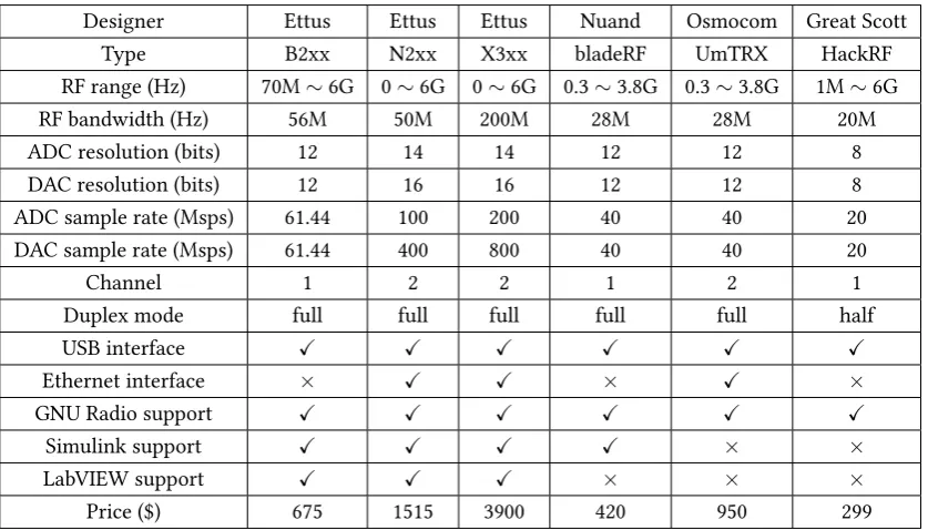
Table 2.2:Comparison on SDR platforms
Designer Ettus Ettus Ettus Nuand Osmocom Great Scott
Type B2xx N2xx X3xx bladeRF UmTRX HackRF
RF range (Hz) 70M∼6G 0∼6G 0∼6G 0.3∼3.8G 0.3∼3.8G 1M∼6G
RF bandwidth (Hz) 56M 50M 200M 28M 28M 20M
ADC resolution (bits) 12 14 14 12 12 8
DAC resolution (bits) 12 16 16 12 12 8
ADC sample rate (Msps) 61.44 100 200 40 40 20
DAC sample rate (Msps) 61.44 400 800 40 40 20
Channel 1 2 2 1 2 1
Duplex mode full full full full full half
USB interface X X X X X X
Ethernet interface × X X × X ×
GNU Radio support X X X X X X
Simulink support X X X X × ×
LabVIEW support X X X × × ×
Price ($) 675 1515 3900 420 950 299
2.3.3
Why is bladeRF chosen?
In this project aVNBwireless communication testbed is built based on bladeRF x40 SDR platform. There are several reasons to choose the bladeRF as SDR platform:
1. The testbed is designed to be operating in the 2.4GISMband. The RF tuning range (0.3∼3.8GHz) of the
bladeRF SDR platform covers the band.
2. The target signal bandwidth is only 1∼10kHz in the testbed. The minimum channel bandwidth of the
bladeRF SDR platform is 1.5MHz. Thus, it is wide enough for the required signal bandwidth in the testbed.
3. The bladeRF SDR platform supports full-duplex communication mode in which the transmission and reception of signal happens simultaneously. Therefore, the transmitter and receiver of the testbed can be implemented on the same bladeRF SDR platform.
4. The bladeRF SDR platform is open-source, well-documented and supported by abundant online tutorials and examples.
5. The bladeRF SDR platform is completely supported by GNU radio.
7. The telecommunication engineering group at the University of Twente possesses the bladeRF SDR platform at hand and it is possible to use the existing experiences from this group regarding the use of the bladeRF platform.
The bladeRF SDR platform that is used in this project is introduced in the next section.
2.3.4
bladeRF Introduction
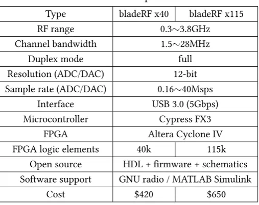
The Nuand bladeRF shown in Fig.2.4is a software-defined radio platform designed to carry out various radio communication experiments. It has a wide tuning range from 300 MHz to 3.8 GHz, covering a wide range of radio frequency spectrum. IndependentTXandRXsignal paths allow the bladeRF to achieve full-duplex communication mode, which means that signal transmission and reception can be conducted simultaneously on the same platform. The USB 3.0 port enables high-speed data transfer between the bladeRFSDR and host computer. Meanwhile, it supports full USB-power supply over the same USB cable. In analog-to-digital or digital-to-analog data conversion, an analog continuous-time signal corresponds to a stream of digital discrete-time samples with each digital sample representing the amplitude of the analog signal at the sampling moment. The sample rate on the bladeRF can be set arbitrarily in the range from 160ksps!up to 40Msps!with
[image:20.595.187.441.485.686.2]every digital sample being 12-bit wide. The bladeRF is able to implement the channel bandwidth from 1.5MHz to 28MHz. In addition, the bladeRF is equipped with high-performance Altera Cyclone IVFPGAon board, which is fully programmable via JTAG port. There are two types of bladeRF, each of which has a different number of logic elements (LE)s in itsFPGA. BladeRF x40 has an FPGA with 40kLEs while bladeRF x115 has an FPGA with 115kLEs [35]. There are two extensible gold-plated RF subminiature version A (SMA) connectors on the bladeRF platform, which can be used for external RFTXandRXantenna ports. The device driver for the bladeRF platform is stably compatible with the mainstream Linux, Windows and Mac operating systems. The last but not least, the bladeRFSDRplatform is supported by many popular third-partySDRdevelopment kits such as GNU radio and MATLAB Simulink. The main technical specifications of bladeRF platform are listed in Table2.3.
Table 2.3:bladeRF specifications
Type bladeRF x40 bladeRF x115
RF range 0.3∼3.8GHz
Channel bandwidth 1.5∼28MHz
Duplex mode full
Resolution (ADC/DAC) 12-bit
Sample rate (ADC/DAC) 0.16∼40Msps
Interface USB 3.0 (5Gbps)
Microcontroller Cypress FX3
FPGA Altera Cyclone IV
FPGA logic elements 40k 115k
Open source HDL + firmware + schematics Software support GNU radio / MATLAB Simulink
CHAPTER 2. EXPERIMENT PLATFORM 14
Figure 2.4:Nuand bladeRF software-defined radio platform [36]
2.3.5
bladeRF Internal Structure
The architecture within the bladeRF is illustrated in Fig. 2.5. The following paragraphs will briefly discuss the functionalities of main blocks in the bladeRF architecture.
Figure 2.5:Nuand bladeRF architecture [35]
The USB 3.0 port is the interface between a host computer and the bladeRF platform with up to 5Gbps high-throughput. This USB port is also backwards compatible with USB 2.0 (480Mbps) but has some sample rate limitations. The resolution of theADCorDACon the bladeRF is 12-bit. The theoretical maximum sample rate on the bladeRF is 40 Msps!. As a result, the maximum bit rate via USB port should be40M×12 = 480M bps.
But, in practice, many host computers which only support USB 2.0 port can not fully achieve the maximum USB 2.0 throughput (480Mbps) so that theADCorDACon the bladeRF is unable to reach its maximum sample rate (40Msps). In addition, the USB port can also deliver power to the bladeRF while it is transferring data. For those who want to run the bladeRF standalone, the bladeRF also supports 5V DC power input jack.
The FPGA not only provides the interface between the Cypress FX3 USB 3.0 controller and the Lime Micro LMS6002D RF transceiver but also carries out additional signal buffering and processing as well as control on the LMS6002D RF transceiver. The data is communicated through independent RXIQ (for receive IQ signal) and TXIQ (for transmit IQ signal) paths between the FPGA and the RF transceiver, enabling the bladeRF platform to work in full-duplex mode. The Altera FPGA on the bladeRF possesses embedded hardware 18×18
multipliers and many general logic elements for custom digital signal processing and hardware acceleration. Since the bladeRF is designed to be fully programmable, all firmware codes for the Cypress controller and VHDL codes for the FPGA logic are available for free modification. allows The Cypress controller and the Altera FPGA on the bladeRF platform can be reprogrammed through JTAG port or USB port. With the free development tool suites provided by the hardware vendors (Cypress and Altera), controller firmware and FPGA logic can be easily customized to fulfill special signal processing tasks.
A voltage-controlled and temperature-compensated crystal oscillator (VCTCXO) in the bladeRF is running at 38.4MHz and supplying a stable frequency reference with the accuracy of±1 ppm for the Cypress controller
and the SI5338 clock generator. The 16-bitDACbefore the crystal oscillator (VCTCXO) provides precise voltage control on the VCTCXO to allow precise tuning of the frequency reference output from VCTCXO. The Silicon Labs SI5338 clock generator synthesizes highly-accurate and low-jitter clock signals for the Altera FPGA and the Lime Micro RF transceiver. TheADCandDACwithin the RF transceiver are driven by clocks from the SI5338 clock generator so that the flexible setting ofADCorDACsample rate is possible on the bladeRF.
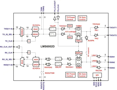
The core component in the bladeRF SDR platform is the Lime Microsystems LMS6002D field programmable RF transceiver chip, which is placed in a silver electromagnetic interference (EMI) shield as shown in Fig.2.4. The EMI shield is designed to protect the RF transceiver from the outside electromagnetic interference and meanwhile to minimize the amount of electromagnetic interference radiated by the RF transceiver. Since the LMS6002D RF transceiver chip contains all of the amplifiers, mixers, filters,ADCandDAC, it performs all of the RF front-end tasks such as gain control, mixing, filtering and A/D or D/A conversion. The RF antennas can be directly connected with the LMS6002D transceiver for RF signal transmission [36], [37].
2.4
LMS6002D Transceiver
2.4.1
Introduction
The most pivotal component in bladeRFSDRplatform is the Lime Microsystems LMS6002D RF transceiver. It is aFPRF transceiverICcontainingLNA, PA, TX/RX mixer, LPF, TX/RX variable-gain amplifier (VGA) andADC/DAC. It converts digital baseband signal up to analog RF signal for radio transmission or converts received analog RF signal down to digital baseband signal for further signal processing.
CHAPTER 2. EXPERIMENT PLATFORM 16
Table 2.4:The specifications for LMS6002D transceiver
Type LMS6002D
RF range (GHz) 0.3∼3.8
Channel bandwidths (MHz) 1.5, 1.75, 2.5, 2.75, 3, 3.84, 5, 5.5, 6, 7, 8.75, 10, 12, 14, 20, 28
Duplex mode full
ADC dual 12-bit paths
DAC dual 12-bit paths
2.4.2
Internal Structure
The LMS6002D RF transceiver whose internal architecture is depicted in Fig.2.6has two independent signal paths: transmit (TX) path and receive (RX) path. Each signal path has its own mixer that is driven by its own phase-locked loop (PLL)s (TXPLL or RXPLL). Although both the TXPLL and RXPLL share the same exter-nal reference clock source (PLLCLK), they can independently generate different carrier frequencies between 0.3 and 3.8GHz for their own mixer. EachPLLproduces a pair of cosine carriers with 90 degrees of phase difference. The TX and RX signal paths are explained in the following.
Figure 2.6:LMS6002D architecture [39]
• Transmit Path:
identifies I and Q samples from a stream of IQ samples on the TX data bus (TXD). When an I sample appears on the TX data bus (TXD), the IQ select-flag-bit (TX_IQ_SEL) is set to 1, controlling the de-multiplexer to push the I sample to the in-phase DAC (IDAC). When a Q sample is available on the TX data bus (TXD), the IQ select-flag-bit (TX_IQ_SEL) is set to 0, controlling the de-multiplexer to push the Q sample to the quadrature DAC (QDAC).
The IQDACis made up of a 12-bit IDAC and a 12-bit QDAC. The IQ DAC sample rate varies from 0.16∼40MHz,
meaning that the IQ DAC is capable of converting 0.16∼40M I and Q samples per second. Since an IQ sample
is the combination of an I sample and a Q sample, the input IQ sample rate is the half of the IQ DAC sample rate, ranging from 0.08∼20MHz. After the IQ DAC, the digital I and Q samples become analog I and Q ones.
The TXLPFdelimits the bandwidths of I and Q baseband signals and smoothens the waveforms of I and Q baseband signals. The LPF has 16 selectable bandwidths, spanning from 0.75∼14MHz. Hence, after the TX
LPF, the bandwidth of the I or Q baseband signal is limited in the range of 0.75∼14MHz. Since the passband
bandwidth of the channel is double the bandwidth of the I or Q baseband signal, the channel bandwidth is in the range of 1.5∼28MHz.
On the TX branch there are two variable-gain amplifiers (TXVGA1 and TXVGA2), whose amplification gains can be configured by internal registers. TXVGA1, which is implemented on the I and Q branches, amplifies the I and Q baseband signals. Located between TXVGA1 and TXVGA2 is the TX mixer. After being amplified by the TXVGA1, the I and Q signals are mixed with the outputs of the transmitPLL(TXPLL) to up-convert both the I and Q baseband signals to the IQ-modulated RF signal. The RF signal is then split into two TX RF branches and amplified by TXVGA2, which serves as TX power amplifier (PA). There are two RF output ports (TXOUT1 and TXOUT2) for RF signal transmission but only one of them is active at any time.
• Receive Path:
Along theRXpath, there are three different RF input ports (RXIN1, RXIN2 and RXIN3) for multi-band recep-tions. RXIN1 receives 0.3∼2.8GHz RF signal input. RXIN2 receives the RF signal in the range of 1.5∼3.8GHz.
RXIN3 is the input port for 0.3∼3.0GHz RF signal.
On the RX branch, there are three amplifiers: RXLNA, RXVGA1 and RXVGA2. The received RF signal is usually weak. So, it is first amplified by low-noise amplifier (RXLNA). Next, the RF signal is mixed with the outputs of the receivePLL(RXPLL) to down-convert the IQ-modulated RF signal to I and Q baseband signals. The variable-gain amplifier (RXVGA1) is intended for automatic gain control (AGC) to clamp the amplitudes of the I and Q baseband signals within a suitable level. Then, the I and Q baseband signals pass through RX low-pass filter (RXLPF). The RXLPF restricts the bandwidths of the I and Q baseband signals, allowing the I and Q signals within the selected bandwidth to pass through while rejecting the I and Q signals outside the chosen bandwidth.
The IQADChas a certain dynamic range between its noise floor and its maximum level of the input am-plitude. In a communication system, the signal strength may vary dramatically. If the signal strength is too small, the signal may get overwhelmed by the quantization noise of the ADC. Conversely, if the signal strength is so large that it goes beyond the maximum input level of the ADC, it may result in the saturation of the ADC output. Therefore, prior to the IQ ADC, the I and Q baseband signals have to go through another automatic gain control performed by RXVGA2 in order to further limit the I and Q signal amplitudes within the dynamic range of the ADC. Like the IQ DAC, the IQ ADC also consists of a 12-bit in-phase ADC (IADC) and a 12-bit quadrature ADC (QADC). An I sample and a Q sample constitutes an IQ sample. The IQ ADC allows the sample rate between 0.16∼40MHz. In other word, the IQ ADC can produce 0.08∼20M digital IQ
samples per second or equivalently 0.16∼40M digital I and Q samples per second.
CHAPTER
3
TRANSMITTER DESIGN
In this chapter, the design of the transmitter will be explained in detail. This chapter will start with giving an overview about the transmitter structure. Then, follows the discussion of BPSK modulator where incoming binary bits are mapped into complex symbols. The rest of this chapter will explain the following issues. How are the complex symbols encoded by double differential encoder? Why do the encoded symbols pass through the repeater? How is IQ modulator working?
3.1
Transmitter Structure Overview
The transmitter part is made up of several blocks as shown in Fig.3.1.
• Random signal source generates a stream of random binary bits to be transmitted.
• BPSK modulator maps a stream of binary bits (1’s and 0’s) into a stream of complex symbols (-1+0j and 1+0j).
• Double differential encoder encodes a stream of complex symbols (1+0j and -1+0j) and outputs an en-coded sequence of complex symbols.
• Repeater takes in a complex symbol with one complex sample per symbol. After repeating an incoming sample N times, it outputs a complex symbol with N complex samples per symbol.
• IQ modulator accepts a complex sample and splits it into real part (in-phase component) and imagi-nary part (quadrature component). Both the in-phase and quadrature components are converted by ADCfrom digital domain to analog domain. Then, both the in-phase and quadrature signals are up-converted to RF signal that is transmitted via antenna. In contrast with the preceding blocks which are implemented by software, the IQ modulator is implemented bySDRplatform.
Figure 3.1:Transmitter block diagram
The following sections will present the detailed insights into BPSK modulator, double differential encoder and repeater. Working principle of IQ modulator/demodulator is explicated in appendixA.
3.2
BPSK Modulator
The phase shift keying (PSK) modulation is a digital modulation method which conveys information bits by the phase of a modulated signal. ThePSKmodulator maps information bits into a finite number of phases while the IQ modulator mixes thePSK-modulated signal with the carrier. After the IQ modulator, the carrier signal to be transmitted contains several phases.
Leti(t)be the information bit from the signal source at any time instanttwhilex(t)denotes the complex symbol output byPSK modulator at time t. The relation betweenx(t)and i(t) can be expressed in the following equations:
φ(t) =2π·i(t)
M i(t) = 0,1· · ·M −1 (3.1)
x(t) =A·ej·φ(t) (3.2)
whereAis the magnitude of the complex symbol,φ(t)denotes the phase that is mapped fromi(t)andM
refers to the modulation order. The orderM determines the number of different symbols that a modulation
scheme can transmit. LetNdenote the number of bits that a symbol conveys. NandMhave the following
relation:
N = log2M (3.3)
For binary phase shift keying (BPSK) modulation scheme,M = 2andN = 1bit/symbol. So, theBPSK
scheme can transmit two different complex symbols with each symbol standing for one bit. For quadrature phase shift keying (QPSK) modulation scheme,M = 4andN = 2bits/symbol. So, theQPSKscheme can
transmit four different complex symbols with each symbol representing two bits.
According to (3.1),BPSKscheme has two complex symbols whose phases are0andπ. According to (3.2)
and assuming unit magnitude (A = 1) for each complex symbol for simplification, the outputx(t)of the
BPSKmodulator in Fig.3.1is expressed as follows:
x(t) =ej·φ(t)
= cosφ(t) +j·sinφ(t)
=
1 +j0 i(t) = 0
−1 +j0 i(t) = 1 (3.4)
The real and imaginary parts of a complex symbolx(t)at timetare called in-phase componentI(t)and quadrature componentQ(t)respectively:
I(t) =Re{x(t)}= cosφ(t) =
1 i(t) = 0
−1 i(t) = 1 (3.5)
Q(t) =Im{x(t)}= sinφ(t) = 0 (3.6)
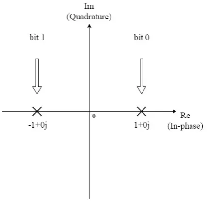
The constellation diagram of BPSK in Fig.3.2reveals the mapping relationship between information bits and complex symbols. The bits 0 and 1 are mapped into the complex symbols1 + 0jand−1 + 0j. Both the
CHAPTER 3. TRANSMITTER DESIGN 20
Figure 3.2:BPSK mapping
In allPSKschemes, BPSKis the simplest one since there are only two symbols used. Compared with otherPSKschemes, the distance between different symbols is the largest inBPSKscheme. As a result, BPSK demodulator can make a correct detection on a symbol while tolerating the highest level of signal distortion and background noise. However, BPSK is only able to modulate 1 bit per symbol. Thus, it is not a suitable choice for high bit-rate transmission [40].
On one hand, this transmitter is applied for wireless transmission at very-low bit rate under strong in-terference and background noise. On the other hand,BPSKscheme can achieve a required lowBERwith less power while other high-orderPSKschemes need more power to maintain the sameBER. Therefore, the BPSKis selected as the modulation scheme. Besides, the BPSK scheme leads to simpler differential encoder and decoder.
3.3
Double Differential Encoder Design
Due to the presence of an arbitrary and unknown phase shift that is introduced by the communication chan-nel, the received symbols may contain a phase offset. It means that the received constellation points are rotated by a phase angle. If the phase angle is greater than 90 degrees, the constellation points fall onto the opposite-half of complex plain. As a result, the BPSK demodulator is unable to distinguish the correct con-stellation points. In order to overcome the phase offset, a differential encoder is needed prior to IQ modulator. Furthermore, due to mismatch between transmitter and receiver’s local oscillators, there is usually a quency offset in the down-converted baseband signal at receiver side. Another reason which results in fre-quency offset is communication channel, which introduces a random frefre-quency shift into the carrier signal because of Doppler effect or channel fading. The introduced frequency offset will constantly rotate the re-ceived constellation points over time, resulting in incorrect symbol detection by BPSK demodulator. A single differential encoder is sensitive to frequency offset. Thus, another single differential encoder is needed to eliminate the frequency offset, resulting in a double differential encoder.
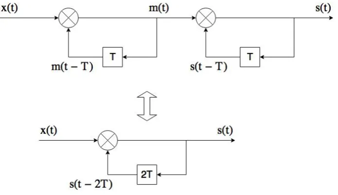
The double differential encoder is composed of two single differential encoders which are connected in series as illustrated in Fig.3.3. Each single differential encoder outputs a complex symbol which depends not only on the current input symbol but also on the previous output symbol.
BPSK-modulated complex signal,m(t)ands(t)also take values +1 or -1.
Figure 3.3:Double differential encoder structure
The output signals(t)is derived from the second encoder.
s(t) =s(t−T)·m(t) (3.7)
From (3.7), we can get:
s(t−T) =s(t−2T)·m(t−T) (3.8) The intermediate signalm(t)is derived from the first encoder.
m(t) =m(t−T)·x(t) (3.9)
Substituting (3.8) and (3.9) into (3.7) while considering thatm(t)·m(t) = 1, we have:
s(t) =s(t−2T)·m(t−T)·m(t−T)·x(t)
=s(t−2T)·x(t) (3.10)
Hence, the two structures in Fig.3.3are equivalent according to the above derivations [41] [42]. For BPSK-modulated signals, a single differential encoder with the delay of two symbol periods2T can supplant two
cascaded single differential encoders with the delay of one symbol periodT to implement double differential
encoding and meanwhile simplify the structure. With regard to how the double differential encoder and decoder are working together to remove phase and frequency offsets, please refer to the appendixB.
3.4
Repeater
The repeater repeats each incoming sample several times. Before the repetition, every symbol is represented by a sample. After the repetition by an integer factor N, every symbol is represented by N samples. The purpose of the repeater is to adjust the symbol rate1on the testbed.
CHAPTER 3. TRANSMITTER DESIGN 22
The whole communication testbed has a definite sample rate (or sample frequency)fsamplewhich is deter-mined byADCandDAC. As a result, the sample durationTsample= f 1
sample is fixed.
LetTsymbol be the symbol duration andRsbe the symbol rate (or symbol frequency). The symbol rate (sometimes called baud rate) is the number of symbols which are transmitted per second through the com-munication channel. Before the repetition, one symbol contains one sample.
Tsymbol=Tsample (3.11)
Thespsis referred to as the number of samples per symbol. After the repetition by an integer factorsps,
one symbol includesspssamples.
Tsymbol=sps·Tsample (3.12)
The symbol rate (or baud rate) is determined by the sample rate and the number of samples per symbol (sps).
Rs=
fsample
sps (3.13)
The bit rateRbis dependent on the symbol rateRsas well as the number of bits that a symbol can represent. The number of bits that a symbol can represent relies on the modulation scheme in use. ForBPSKmodulation, one symbol represents one bit.
Tbit=Tsymbol=sps·Tsample (3.14)
Rb=Rs=
fsample
sps (3.15)
Listed in Table3.1are several bit ratesRb and correspondingsps(samples per symbol) when the sample ratefsampleis fixed at 80 kHz. As we can see in Table3.1, increasingspsleads to decreasing bit rateRb.
Table 3.1:Bit rate and sps whenfsample= 80 kHz
Rb(bps) sps
10000 8
1000 80
100 800
Lets(t)be the input of the repeater andsN(t)be the output of the repeater. Since the outputsN(t)is a BPSK-modulated complex signal, it has in-phase componentI(t)(real part) and quadrature componentQ(t) (imaginary part) as follows:
I(t) =Re{sN(t)}=±1 (3.16)
Q(t) =Im{sN(t)}= 0 (3.17)
Figure 3.4:Non-return-to-zero pulse in time domain
The in-phase componentI(t)is a train of rectangular pulses in time domain. The Fourier transform ofI(t) isI(f)which is a sinc function in frequency domain. Figure3.5displays the power spectrum forI(f).
Figure 3.5:Power spectrum for non-return-to-zero pulses
The power spectrum|I(f)|2is a sinc function with zero-crossing points at±k·R
bwhere k is any integer andRbis bit rate. Since the main lobe contains most of the pulse energy, the baseband bandwidthBW of the BPSK-modulated signal is equivalent to the bandwidth occupied by the main lobe.
BW =Rb= 1
Tbit
= fsamp
sps (3.18)
Whensps(samples per symbol) increases, one symbol contains more samples and anNRZrectangular pulse
has longer pulse durationTbit. Accordingly, the pulses vary less frequently and the bit rateRbdecreases. The main lobe compresses and the baseband bandwidthBW of the BPSK-modulated signal becomes narrower.
Asspsdecreases, one symbol includes less samples and the pulse durationTbit becomes shorter. Corre-spondingly, the pulses change more frequently and the bit rateRbincreases. The main lobe outspreads and the baseband bandwidthBW of the BPSK-modulated signal becomes wider. To summarize, by adjusting the
parameter ‘sps’ (samples per symbol) in the repeater, transmission at different bit rates can be easily achieved
on the testbed.
3.5
IQ Modulator
The IQ modulator up-converts the baseband signal to theRFpassband with carrier frequencyfc. After that,
CHAPTER 3. TRANSMITTER DESIGN 24
by bladeRFSDRplatform. In GNU Radio, there is a special block called ‘osmocom sink’ which is an interface between the digital baseband signal and the bladeRF. The structure of the IQ modulator is shown in Fig.3.6.
Figure 3.6:IQ modulator structure
The input signalsN(t)to the IQ modulator is a stream of complex samples. In this case, the inputsN(t)is a BPSK-modulated complex signal with information bits stored in phaseφ(t).
sN(t) =ej·φ(t)
=cosφ(t) +j·sinφ(t)
=
1 +j0 φ(t) = 0
−1 +j0 φ(t) =π (3.19)
At first, the complex signalsN(t)is decomposed into real part along the in-phase path and imaginary part along the quadrature path. The in-phase digital-to-analog converter (IDAC) and quadrature digital-to-analog converter (QDAC) perform digital-to-analog conversions on the real and imaginary parts of the signal
sN(t)respectively. After the digital-to-analog conversion, both the real partRe{sN(t)}and imaginary part
Im{sN(t)}become analog signals. Let us assumesN I(t) =Re{sN(t)}andsN Q(t) =Im{sN(t)}:
sN I(t) =Re{sN(t)}=cosφ(t) =±1 (3.20)
sN Q(t) =Im{sN(t)}=sinφ(t) = 0 (3.21)
Figure 3.7:In-phase signal spectrum and its filtered spectrum
Then, the real partSN I(f)passes through theLPFwhere high-frequency side lobes are suppressed while low-frequency main lobe is allowed to pass through. Due to the suppression over the high-frequency side lobes, theLPFoutput along the in-phase pathsI(t)is a train of slightly distorted pulses instead of strictly rectangular pulses in time domain. To be precise, the transition between two different successive pulses (such as -1 up to 1 or 1 down to -1) gets smoother instead of jumping between two discontinuous points. In frequency domain, theLPFoutput does not include high-frequency side lobes but keeps low-frequency main lobe which contains most of the energy and information as shown in Fig.3.7. Hence, theLPFoutputssI(t) andsQ(t)hold the same information contents as the theLPFinputssN I(t)andsN Q(t).
sI(t) =sN I(t) =cosφ(t) =±1 (3.22)
sQ(t) =sN Q(t) =sinφ(t) = 0 (3.23)
After passing through theLPF, the in-phase baseband signalsI(t)and quadrature baseband signalsQ(t) are mixed separately with the in-phase and90o-shifted quadrature carriers which are generated by the local oscillator (LO1). Mathematically, the mixer is treated as a multiplier, performing multiplication in time do-main or convolution in frequency dodo-main. The in-phase signalsI(t)is multiplied with the in-phase carrier
cos2πfctin time domain. In frequency domain, the multiplication turns into convolution operation and the mixed in-phase signalsI(t)·cos2πfctbecomes:
F {sI(t)·cos2πfct} =SI(f)∗[
1
2δ(f+fc) + 1
2δ(f−fc)]
=1
2·SI(f+fc) + 1
CHAPTER 3. TRANSMITTER DESIGN 26
where the spectrum of the in-phase signalsI(t)is split into two parts: one centered at the carrier frequency
[image:33.595.93.529.137.415.2]fc and the other centered at the negative carrier frequency−fc. Figure 3.8illustrates this up-conversion (mixing) process.
Figure 3.8:In-phase signal up-conversion
After mixing, the output RF signalsIQ(t)is the sum of the mixed in-phase and quadrature signals [43].
sIQ(t) =sI(t)·cos 2πfct−sQ(t)·sin 2πfct = cosφ(t)·cos 2πfct−sinφ(t)·sin 2πfct
= cos(2πfct+φ(t)) (3.25)
From (3.25), it can be seen that the output signalsIQ(t)is a cosine wave with carrier frequencyfc and binary phaseφ(t). The information bit (0 or 1) determines the phaseφ(t), which has two values0andπ.
CHAPTER
4
RECEIVER DESIGN
In this chapter, the design of the receiver will be discussed. First of all, the overall structure of the receiver will be presented. Then, five important blocks in the receiver will be discussed separately. They are IQ demodulator, DC-offset compensator, double differential decoder, matched filter and sampler.
4.1
Receiver Structure Overview
In comparison with the transmitter, the receiver structure is far more complicated. The block diagram of the receiver is shown in Fig.4.1. The receiver processes complex samples at baseband, which are the output of the IQ demodulator onSDRplatform. In this diagram, the receiver is composed of several blocks: IQ demodulator, DCoffset compensator, double differential decoder, integrator and BPSK demodulator.
Figure 4.1:Receiver block diagram
The received complex samples pass through a series of functional blocks before being demodulated into information bits. The following part will briefly introduce the basic function of every block in the path:
• IQ demodulator: The IQ demodulator takes in analogRFsignal and down-converts the signal from radio frequency to baseband. Then, the analog baseband signal is converted into digital baseband signal by theADC. It outputs a stream of complex samples. Section4.2presents how IQ demodulator works in detail.
• DC offset compensator: The DCoffset refers to the degree by which the mean value of a group of received samples deviates from zero. Let us take theBPSKsignal as an example. If the absolute value ofDCoffset is so large that all of received complex samples fall on the negative-side or positive-side of constellation diagram, it will bring about incorrect symbol detection and wrong information bits. The
CHAPTER 4. RECEIVER DESIGN 28
DCoffset compensator estimates the mean value of a group of incoming samples and subtracts this mean value from every received sample to correct every sample so that theDCoffset of the received samples stays close to zero. This block improves the accuracy of symbol detection. The details of DC offset compensation will be presented in section4.3.
• First differential decoder: Since phase offset and frequency offset are introduced into received com-plex samples, the first differential decoder removes the already existing phase offset and meanwhile it converts frequency offset into constant phase offset. Section4.4provides the details on how it works.
• Matched filter: In the output of the first differential decoder, each symbol is represented by multiple samples. The matched filter, which is implemented by a moving average filter, integrates successive N incoming samples where N is the number of samples per symbol. It actually matches the pulse shape of the received symbol with the rectangular pulse shape of the transmitted symbol. Its outgoing sample sequence has triangle shapes where the peaky samples are extracted by the following sampler.
• Sampler: The sampler block looks for the peaky samples in the sequence output by the matched filter and samples them for the second differential decoder. The matched filter and the sampler together play a role of integration where all samples per symbol output by the first differential decoder are summed up and the sum result (one sample per symbol) is fed to the second differential decoder. The design details about the matched filter and the sampler are presented in section4.5.
• Second differential decoder: The second differential decoder eliminates the remaining phase offset, which is a result of the frequency offset from the first differential decoder. Section4.4provides the detail explanations on how it works.
4.2
IQ Demodulator
4.2.1
IQ Demodulation
The IQ demodulator is implemented by theSDRplatform. It down-converts the RF signal to baseband signal for further signal processing. Figure4.2exhibits the internal structure of the IQ demodulator. In this testbed, the IQ demodulation work is done in bladeRFSDRplatform. In GNU radio, there exists a special block called ‘osmocom source’, which is an interface between the IQ demodulator in bladeRF and the signal processing blocks in GNU radio .
Figure 4.2:IQ demodulator structure
to the RF signalsIQ(t)that is transmitted from the IQ modulator.
rIQ(t) =sIQ(t) = cos(2πfct+φ(t)) (4.1)
The carrier frequency generated by the local oscillator (LO2) is tuned to befc, which is equal to the
fre-quency of the received RF signalrIQ(t). Firstly, the received RF signalrIQ(t)is split into in-phase path and quadrature path respectively. The RF signal on the in-phase path is mixed with the in-phase carriercos 2πfct while the RF signal on the quadrature path is mixed with the quadrature carrier−sin 2πfct. After mixing, the mixed signals along the in-phase and quadrature paths are formulated as follows:
rIQ(t)·cos 2πfct
= cos(2πfct+φ(t))·cos 2πfct =1
2cosφ(t) + 1
2cos (2π·2fct+φ(t)) (4.2)
rIQ(t)·(−sin 2πfct)
= cos(2πfct+φ(t))·(−sin 2πfct)
=1
2sinφ(t)− 1
2sin (2π·2fct+φ(t)) (4.3)
Both of the mixed signals contain high-frequency contents around2fc. After theLPFs, the high-frequency
components1
2cos (2π·2fct+φ(t))and 1
2sin (2π·2fct+φ(t))are removed from the mixed signals. TheLPF
outputs along the in-phase and quadrature paths arerI(t)andrQ(t)respectively. Since the phaseφ(t)takes the value of0orπ, we get
rI(t) = 1
2cosφ(t) =± 1
2 (4.4)
rQ(t) = 1
2sinφ(t) = 0 (4.5)
The in-phase analog-to-digital converter (IADC) and quadrature analog-to-digital converter (QADC) con-vert the in-phase and quadrature signals from analog domain to digital domain for further signal processing. After theADC, the in-phase signalrI(t)(real part) and quadrature signalrQ(t)(imaginary part) are combined into complex signal. The output of the IQ demodulator is
rN(t) =rI(t) +jrQ(t)
= 1
2(cosφ(t) +jsinφ(t))
= 1
2e
jφ(t) (4.6)
Now we can understand the IQ demodulation from the frequency-domain perspective. From section3.5, it is known that the quadrature baseband signalsQ(t)from the IQ modulator is always zero while the in-phase baseband signalsI(t)from the IQ modulator is a sequence ofNRZpulses (+1 or -1). In frequency domain, the Fourier transform ofsI(t), which is denoted bySI(f), is a sinc function. After passing through a zero-noise channel, the received RF signalrIQ(t)is equal to the transmitted RF signalsIQ(t).
rIQ(t) =sIQ(t)
=sI(t)·cos 2πfct−sQ(t)·sin 2πfct
CHAPTER 4. RECEIVER DESIGN 30
The Fourier transform of the RF signalrIQ(t)is derived as follows:
RIQ(f) =F {rIQ(t)}
=F {sI(t)·cos 2πfct}
= 1
2·SI(f+fc) + 1
2 ·SI(f−fc) (4.8)
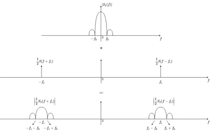
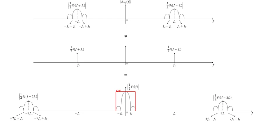
[image:37.595.96.532.246.463.2]In the IQ demodulator, the received RF signalrIQ(t)is split into the in-phase and quadrature paths and then mixed with carrierscos 2πfctand−sin 2πfct. The mixing process down-converts theRFsignalrIQ(t) to the baseband and Figure4.3illustrates the down-conversion process performed by the in-phase mixer. It is noteworthy that the mixing process is a convolution (denoted by∗) in frequency domain.
Figure 4.3:Received RF signal down-conversion
The output of the in-phase mixerrIQ(t)·cos2πfctis expressed in frequency domain as follows:
F {rIQ(t)·cos2πfct} =RIQ(f)∗[
1
2δ(f+fc) + 1
2δ(f −fc)]
=1
2·RIQ(f +fc) + 1
2·RIQ(f−fc)
=1
4·SI(f+ 2fc) + 1
2·SI(f) + 1
4 ·SI(f−2fc) (4.9)
The output of the quadrature mixerrIQ(t)·(−sin2πfct)is formulated in frequency domain as follows:
F {rIQ(t)·(−sin2πfct)} =RIQ(f)∗[−
j
2δ(f+fc) +
j
2δ(f −fc)]
=−j
2·RIQ(f+fc) +
j
2·RIQ(f−fc)
=−j
4·SI(f + 2fc)−
j
4 ·SI(f) +
j
4 ·SI(f) +
j
4·SI(f−2fc)
=−j
4·SI(f + 2fc) +
j
![Figure 1.3: Hardware structure of a wireless sensor node [21]](https://thumb-us.123doks.com/thumbv2/123dok_us/9760380.477071/11.595.255.369.180.338/figure-hardware-structure-wireless-sensor-node.webp)