High-Performance CMOS Current Mirrors: Application
to Linear Voltage-to-Current Converter Used for
Two-Stage Operational Amplifier
Radwene Laajimi, Mohamed Masmoudi
Department of Electrical Engineering Electronics, Micro-Technology and Communication (EMC) Research Group Sfax (ENIS), University of Sfax, Sfax, Tunisia
Email: [email protected]
Received May 3, 2012; revised June 28, 2012; accepted July 5,2012
ABSTRACT
This paper presents two schemes of high performance CMOS current mirror, one of them is used for operational trans-conductance amplifier (OTA) in analog VLSI systems. The linearity, output impedance, bandwidth and accuracy are the most parameters to determine the performance of the current mirror. Here a comparison of two architectures based on same architecture of the amplifier is presented. This comparison includes: linearity, output impedance, bandwidth and accuracy. These two circuits are validated with simulation in technology AMS 0.35 µm. An operational amplifier based on the adapted current mirror is proposed. Its frequency analysis with large bandwidth is validated with the same tech-nology.
Keywords: Analog Circuits; Current Source; Current Mirror; Low Voltage; Operational Transconductance Amplifier
1. Introduction
In the last few years, the demand for analog circuits which can operate at low voltage is an established fact and does not need any further justification. In particular structures of current mirrors which have increased rap-idly and become one of the most interesting areas of re-search [1]. Many configurations of current mirror are discussed and used for many applications. Especially cascode current mirror which is one of the main building blocks of analog and mixed-signal integrated circuits. For low voltage design circuit and high speed application, the important parameters to determine high performance current mirror are [2-4]:
Low input and output voltage.
Low input impedance.
High output impedance.
Minimum error of copying accuracy and settling time. The four transistors circuit shown in Figure 1(a) is a
simple cascode current mirror and it is characterized by moderately low input and output voltages.
Equation (1) of input voltage is:
in 2 DSAT 2 T
V V V
out 2 DSAT T
V V V
(1) Equation (2) of output voltage is:
(2) (VDSAT and VT denote is the minimum drain-source satu-ration voltage and the transistor’s threshold voltage.)
This circuit has higher output impedance than the sim-ple current mirror and moderately high input impedance.
Equation (3) of input impedance is:
in
11 12
1 1
Z
gm gm
(3)
Equation (4) of output impedance is:
9 out
9. 10
gm Z
go go
(4)
(where gm and go are the small-signal transconductance gain and the conductance of the MOS transistor, respec-tively.)
(a)
[image:2.595.81.262.85.536.2](b)
Figure 1. Current mirror configuration. (a) Simple cascode current mirror; (b) Cascode current mirror with regulated voltage.
voltage of M10 and M12 and results in a loss of accuracy, so degraded linearity (due to channel length modulation).
To overcome this limitation, we are proposing two novels structures of current mirror which offers both the low compliance voltage and a minimum error of copying accuracy. The two proposed approaches are based on using a differential amplifier to compare the drain volt-ages of the input and output mirror transistors, to force the equality between these voltages, thereby improving the accuracy of the current copy, and improving linearity.
The paper is organized as follows. The second section presents the amplifiers structures used for voltage to
cur-rent (V-I) converter. In the third section, the design of proposed version 1 of V-I converter is presented with simulations results. The proposed version 2 of V-I con-verter is presented in section four. Section 5 presents an application of V-I converter in two-stage operational amplifier. Conclusion is drawn in the last section.
2. Amplifier Structures
In order to achieve high current copy accuracy, it is nec-essary to use an amplifier between the mirror’s input and output transistors.
The amplifier architectures are: simple differential amplifier [6] and amplifier proposed by [5]. As shown in
Figure 2(a), this structure is formed by the input
differ-ential pair (MP1 and MP2) and the active charge (MN1 and MN2). The Figure 2(b) shows a differential
ampli-fier with two MOS transistors (MN1 and MN2) in which MN1 is operated in the weak version region (source gate voltage of MN1 equal to zero). This version can operate either in the linear region or in the saturation region for achieving low voltage and low consumption.
Moreover, the amplifier, which has many transistors, causes the increase of the power dissipation and the chip area. The advantages of the scheme proposed by [7] are low voltage operation, small chip area, high output resis-tance and no bias current. For this reason we use this structure in our two versions of voltage to current con-verter which are more described in the following para-graph.
MP1
MP2
MN2
MN1
Vdd
Vss
1 2
3
MN2 Vdd
MN1
1 3
2
(a) (b)
3
[image:2.595.313.531.447.691.2]2 1
3. Proposed Version 1 of Voltage to
Current Converter
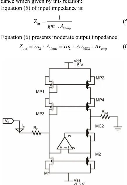
3.1. Description
According to Figure 3 the version 1 of V-I converter is
composed of three blocks: polarisation, correction and output load.
The polarisation block is formed of four transistors (MP1, MP2, MP3, MP4) with variable input voltage Vin
and input resistance Rin. The correction block is
com-posed of three transistors (M1, M2, MC2). It character-ized by minimum error of copying accuracy due to the equality of drain source voltage between M1 and M2. This equality thanks to an amplifier between the mirror’s input and output transistors M1 and M2 and causes high accuracy and good linearity. High output impedance is obtained by the output current of amplifier and passes to the gate of transistor MC2. The output load block is a simply resistance (Rout).
This scheme offers a comparison between drain source voltage of M1 and M2 by using a differential amplifier to provide higher accuracy of the current copy. The input injection current signal Iin is replaced by another source
formed by variable input voltage Vin with resistance Rin.
On the one hand, we obtain a reduction of the input im-pedance which given by this relation:
Equation (5) of input impedance is:
in
Z
1 olinp
1 .
gm A
MC2 omp
(5)
Equation (6) presents moderate output impedance
out 2 olout 2
Z ro A ro Av Av (6)
Figure 3. Proposed version 1 of voltage to current con-verter.
where gm and ro are the small-signal transconductance gain and the output resistance of the MOS transistors. In this case we assume that the amplifier have an input open-loop gain Aolinp and output open-loop gain Aolout
(Aolout = AvMC2·Avomp). AvMC2 and Avomp denote the
volt-age gain of the transistor MC2 and amplifier gain respec-tively.
On the other hand, the drain source voltage of the mirror transistor M1 achieves a small constant value thanks to current source Iin and variable voltage source
Vin. Drain source voltage can be decreasing to a
mini-mum value, by selection of Vin and consequently a very
low input voltage of the circuit.
3.2. Simulations Results
Different schemes are simulated using Tspice based on BSIM3V3 transistor model for the technology AMS 0.35 µm at ±1.5 V power supply voltage.
Tspice simulations are carried for an input voltage Vin
varied from −1.1 V to 0 V, Figure 4 shows the DC
char-acteristic for the V-I converter for different values of resistance (Rout = 100 Ω, Rout = 1 KΩ, Rout = 5 KΩ) in
which the full input voltage swing capability is evident with truly linearity.
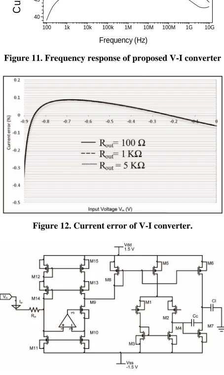
As shown in Figure 5, from DC output characteristics
simulations, the output resistance presents a moderate value of 0.18 MΩ.
The Figure 6 shows the AC characteristic of the
pro-posed V-I converter. For a resistance of 100 Ω, we
achieved a common gain bandwidth (GBW) equal to 750 MHz for different values of resistance (Rout = 100
Ω, Rout = 1 KΩ, Rout = 5 KΩ) and variable gain (Av) from
53 dB to 80.2 dB at minimum resistance (Rout = 100 Ω).
According to Figure 7, the deviation of the DC output
current from the ideal characteristic for different values of resistance Rout. The large error is reached for the
low-est input voltage Vin of −1.1 V. On the other hand the
variation of Vin between −0.9 V to 0 V provide a small
current error under 0.1% for different values of resistance (Rout = 100 Ω, Rout = 1 KΩ, Rout = 5 KΩ). Moreover for
the maximum current error of 0.5%, Vin varied from −1.1
V to −0.95 V in particular for output resistance Rout = 5
KΩ.
4. Proposed Version 2 of Voltage to
Current Converter
4.1. Description
The version 2 of V-I converter is presented in Figure 8. It
is like the structure of version 1 shown in Figure 3 and
[image:3.595.65.283.390.708.2]-1.1 -1.0 -0.9 -0.8 -0.7 -0.6 -0.5 -0.4 -0.3 -0.2 -0.1 -0.0
Vin (V) 0
50 100 150
R
R
R
out= 100 Ω out= 1 KΩ out = 5 KΩ
For Vin = - 1V Iout=10µA
Ou
tp
ut
C
urre
nt
(
μ
A)
[image:4.595.78.265.82.225.2]Vin (v)
Figure 4. DC characteristics of V-I converter for different values of resistance Rout.
-1.5 -1.0 -0.5 0.0 0.5 1.0 1.5
Vout (V) 0
10 20 30 40 50 60 70
(-1.00, 57.16u) (1.30, 69.17u) dx=2.30 dy=12.01u m=5.22u
Meg 18 . 0
out out out
I V R
Ou
tp
ut
C
urre
nt
(
μ
A)
[image:4.595.319.525.83.307.2]Vout (v)
Figure 5. Output current vs output voltage variation of proposed V-I converter.
Cu
rr
e
n
t Ga
in
(
d
B
)
100 1k 10k 100k 1M 10M 100M 1G 10G
Frequency (Hz) 45
50 55 60 65 70 75 80
Rout= 100 Ω
Rout= 1 KΩ
Rout = 5 KΩ
Figure 6. Frequency response of proposed V-I converter.
Figure 7. Current error of V-I converter.
Figure 8. Proposed version 2 of voltage to current con-verter.
with an amplifier between M1 and M2 in order to mini-mise error of copying accuracy.
In this case of structure an approach is used to increase the output impedance without sacrificing the equality between input and output of drain source voltage (M1 and M2), consists in integrating a connection between the gate of transistor MC2 and the gate of transistor M2. We achieved very high output impedance due to the output current of amplifier. This current is passed through each gate of transistors MC2 and M2. Equation (8) shows the value of output impedance which is:
Zoutro2 Aolout ro2 AvMC2AvM2Avomp (8)
olout MC2. M2. omp
ro2 denote the output resistance of the MOS transistor
M2. The amplifier has an output open-loop gain Aolout.
Equation (9) give this relation:
A Av Av Av (9)
We assume that AvMC2, AvM2 and Avomp denote the
voltage gain of the transistor MC2, M2 and amplifier gain respectively.
4.2. Simulations Results
From Tspice simulations, an input voltage Vin varied
from −1 V to 0 V, the DC characteristic for the V-I con-verter for different values of resistance (Rout = 100 Ω, Rout
= 1 KΩ, Rout = 5 KΩ) is shown in Figure 9. We find that
the linearity is evident for each value of resistance. To confirm the high output resistance given by the proposed version 2 of V-I converter, Figure 10 shows
[image:4.595.76.271.263.401.2] [image:4.595.79.273.440.579.2] [image:4.595.58.287.605.716.2]-1.0 -0.9 -0.8 -0.7 -0.6 -0.5 -0.4 -0.3 -0.2 -0.1 -0.0
Vin (V) 0
50 100
Rout= 1
Rout= 1
Rout
00 Ω KΩ = 5 KΩ For Vin = - 0.85 V Iout=10µA
Ou
tp
ut
C
urre
nt
(
μ
A)
[image:5.595.67.279.85.228.2]Vin (V)
Figure 9. DC characteristics of V-I converter for different values of resistance Rout.
-1.5 -1.0 -0.5 0.0 0.5 1.0 1.5
Vout (V) 0
5 10 15 20 25 30 35 40 45 50 55
(1.30, 55.75u) (-1.00, 49.02u) dx=-2.30 dy=-6.73u m=2.92u
Meg 34 . 0
out out out
I V R
O
utp
ut
C
urre
nt
(
μ
A)
[image:5.595.319.527.228.377.2]Vout (V)
Figure 10. Output current vs output voltage variation of proposed V-I converter.
From AC characteristic, we note an improvement of the gain (Av). Its maximum value is 73 dB but it is 80.2 dB for the proposed version 1 of V-I converter. The bandwidth responses for different values of resistance are presented in Figure 11.
From Figure 12, we present a current error of V-I
converter for different values of resistance Rout. On the
one hand, the variation of Vin from −0.9 V to 0 V give the
same characteristic of error for different values of resis-tance (Rout = 100 Ω, Rout = 1 KΩ, Rout = 5 KΩ). On the
other hand for the maximum current error of 0.35%, Vin
is lower than −0.95 V.
5. Application of V-I Converter in
Two-Stage Operational Amplifier
Voltage to current V-I converter becomes the most inter-esting element of interface measurement in the field of mixed signal systems [8].
The most important parameters to determine high per-formance of current V-I converters are:
High linear range.
Large bandwidth and gain.
Because the large bandwidth and gain of the proposed
version 1 of V-I converter, it is possible to use this ap-proach for Operational amplifier[9,10]. The Figure 13
shows a practical implementation of the two-stage Op-erational amplifier.
The simulated output frequency response of our appli-cation is shown in Figure 14. The bode diagram gives an
open loop gain of 60 dB with a large GBW of 82 MHz, a 97 KHz of cut-off frequency and a phase margin of 62˚. We note that the input current passes through M8 using for polarisation is equal to 10 µA and this corresponds to an input voltage Vin of −1 V.
Cu
rr
e
n
t G
a
in
(
d
B
)
100 1k 10k 100k 1M 10M 100M 1G 10G
Frequency (Hz)
40 45 50 55 60 65 70
Rout= 100 Ω
Rout= 1 KΩ [image:5.595.70.279.265.411.2]
Rout = 5 KΩ
Figure 11. Frequency response of proposed V-I converter
Figure 12. Current error of V-I converter.
[image:5.595.309.536.332.712.2] [image:5.595.310.536.409.569.2] [image:5.595.307.540.580.705.2]100 1k 10k 100k 1M 10M 100M
Frequency (Hz) -100
-50 0 50
M
agni
tude (dB
),
P
has
e
(deg
[image:6.595.74.271.86.234.2])
Figure 14. Frequency response of proposed V-I converter.
6. Conclusion
Current mirror play an important role in analog circuits used for V-I converter. This work presents two novels design of V-I converter. The version 1 of V-I converter is implemented in Two-Stage Operational Amplifier. How- ever the version 2 gives high output impedance. The use of version 1 due to its large bandwidth of 750 MHz and gain of 80.2 dB. Simulations results of application of V-I converter in two-stage operational amplifier indicated that phase margin is 62˚ to ensure a good stability, gain of 60 dB for ±1.5 V, and GBW of 82 MHz.
REFERENCES
[1] M. H. Li and H. L. Kwork, “The Application of Current- Mode Circuits in the Design of an A/D Converter,” IEEE Canadian Conference on Electrical and Computer Engi- neering, Vol. 1, 1998, pp. 41-44.
[2] K.-H. Cheng, C.-C. Chen and C.-F. Chung, “Accurate Current Mirror with High Output Impedance,” 8th IEEE International Conference Electronics on Circuits and
Systems, Vol. 2, 2001, pp. 565-568.
[3] K.-H. Cheng, T.-S. Chen and C.-W. Kuo, “High Accu-racy Current Mirror with Low Settling Time,” Proceed-ings of the 46th IEEE International Midwest Symposium on Circuits and Systems, Vol. 1, 2003, pp. 189-192.
[4] M. S. Sawant, J. Ramirez-Angulo, A. J. Lopez-Martin and R. G. Carvajal, “New Compact Implementation of a Very High Performance CMOS Current Mirror,” 48th Midwest Symposium on Circuits and Systems, Vol. 1,
2005, pp. 840-842.doi:10.1109/MWSCAS.2005.1594232 [5] J. Ramirez-Angulo, R. G. Carvajal and A. Torralba, “Low Supply Voltage High Performance CMOS Current Mirror with Low Input and Output Voltage Requirements,” IEEE Transactions on Circuits and Systems-II Express Briefs,
Vol. 51, No. 3, 2004, pp. 124-129.
[6] A. N. Mohieldin, E. Sánchez-Sinencio and J. Silva- Martínez, “Nonlinear Effects in Pseudo Differential OTAs with CMFB,” IEEE Transactions on Circuits and Systems-II: Analog and Digital Signal Processing, Vol.
50, No. 10, 2003, pp. 762-770.
[7] K. tanno, O. Ishizuka and Z. Tang, “Low Voltage and Low Frequency Current Mirror Using a Two-MOS Sub-threshold op-amp,” Electronics Letters, Vol. 32, No. 7,
1996, pp. 605-606.
[8] V. Srinivasan, R. Chawla and P. Haster, “Linear Current to Voltage and Voltage to Current Converters,” 48th Midwest Symposium on Circuits and Systems, Vol. 1,
2005, pp. 675-678.
[9] B. H. Soni and R. N. Dhavse, “Design of Operational Transconductance Amplifier Using 0.35 μm Technol-ogy,” International Journal of Wisdom Based Computing,
Vol. 1, No. 2, 2011, pp. 28-31.
![Figure 2. Amplifier configuration. (a) Simple differential amplifier structure [6]; (b) Two-transistor apmlifier struc-ture [7]](https://thumb-us.123doks.com/thumbv2/123dok_us/9976292.498289/2.595.313.531.447.691/figure-amplifier-configuration-differential-amplifier-structure-transistor-apmlifier.webp)