High Voltage CUK Based DC-AC Converter for
Renewable Energy Resources Using VLSI Module
Padmarasan. M1, Manimurugan. M2, Aravindhan. B3, Chanthru. E4, Devanand. K5, Devanathan. S6 1, 2, 3, 4, 5, 6
First-Sixth Department of Electrical and Electronics Engineering, First-Sixth Panimalar Institute of Technology. Chennai
Abstract: In this thesis, an improved structure of modified CUK converter (MCCVLSI) is presented using Voltage Lift Switched Inductor (VLSI) module. The proposed converter provides a negative high DC voltage which is then converted into AC supply using inverter domestic applications. A three new modified CUK converter structures are derived with the help of VLSI module as; MCCVLSI-XLL, and MCCVLSI-LLZ. The complete mathematical analysis is provided to calculated voltage conversion ratio. Moreover, the proposed structures are compared with each other’s in terms of voltage conversion ratio and number of components. The working mode of MCCVLSI-XLL is explained in details. The qualities of the presented structures are reviewed in details. The simulation results are provided and the obtained results show a good agreement with theoretical analysis. The proposed scheme is simple and easy to implement.
Keywords: Modified Cuk Converter; Voltage Lift Technique; Negative Output; High Voltage; DC-AC; Renewable Energy
I. INTRODUCTION
In recent years, many power electronics researchers are engaged to find a new converter structure to utilize renewable energy sources efficiently. Due to free of cost, availability, plentiful in nature, pollution free and advancement in technologies, many researcher claims that photovoltaic is one of the leading energy sector . The output terminal voltage of photovoltaic cell is low and thus series-parallel arrangement of photovoltaic cells is used to achieve required high voltage and high current. But series connection of photovoltaic cells is not suitable technique to achieve high voltage due to large number of photovoltaic cell requirement. A converter is necessary, which step-up the output voltage according to requirement. As a result, DC to DC power converter plays the important block in photovoltaic system. Based on the input and output terminals, DC to DC power converters are categorized into two types; isolated and non-isolated. In isolated structure of DC-DC converter, transformer and coupled inductors are utilizing to isolate the input and output terminal. These converters provides a higher voltage at the output port by utilizing proper transformer windings turns ratio and coupling ratio of coupled inductors . However, size, cost and bulkiness of the converter is increases due to utilization of transformer and coupled inductor. Furthermore, the efficiency of converter is reduced due to Electromagnetic Interference (EMI) and leakage inductance of transformer.
Recently several non-isolated converters structures are proposed with high conversion ratio, higher efficiency and without using transformer and coupled inductor. Thus, size and bulkiness of power converter is reduced. Traditional buck and boost converters are the two types of DC to DC converter which provides positive output voltage and designed by using single inductor, switch and diode arrangement. To combine the feature of buck and boost converter, a new arrangement is designed called buck-boost converter. Buck- boost converter provides a negative output voltage with step- down and step-up capability. The discontinuous input current is the main drawback of boost converter which proves the less utilization of input source. To overcome the downside of buck-boost converter, derived converters (CUK, SEPIC and Zeta) are proposed by hybridization of traditional buck, buck-boost and buck-buck-boost converter. CUK converter provides a negative output voltage with continuous output and input current. But the voltage conversion ratio of these converters is low; due to this reason modification in CUK converter is required to step-up the voltage with large conversion ratio. Quadratic and cascaded boost converter is employed to achieve high voltage but, large number of inductor and synchronization of several switches is main drawback of these converters.
structure of CUK converter (MCC) is presented by combining the features of boost and CUK converter. This CUK converter structure provides an inverting voltage with high voltage conversion ratio compared to traditional DC-DC converter.
In this thesis, new two converter structures are derived to enhance the voltage generated from renewable energy source with high value. The presented converter provides a higher voltage conversion ratio compared to MCC.
II. MODIFIED CUK CONVERTER STRUCTURES WITH VLSI MODULE (MCCVLSI)
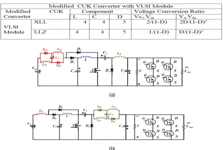
[image:2.612.161.449.214.367.2]The modified CUK converter is shown in Fig. 1. To achieve high voltage conversion ratio, a VLSI module is adopted in MCC. The proposed work is extension of [19]. The VLSI module is placed on position of inductor LX called as Modified CUK Converter with XLL configurations (MCCVLSIXLL). Similarly, and in (MCCVLSI-LLZ), VLSI module is replaced on position of inductor LZ as shown in Fig. 2 (a)-(c). The VLSI module consists of one capacitor, two diodes and two inductors.
[image:2.612.83.529.412.712.2]Fig. 1 Modified Cuk Converter with VLSI module (MCCVLSI)
TABLE I. PROPOSED CONVERTER
(a)
(b)
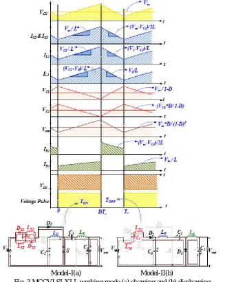
A. Operation of MCCVLSI Structure
The operating mode of three proposed converter structures is similar to each other. To understand the working of the proposed converter structures, the operation of MCCVLSI-XLL is explained in detail. In conducting state of switch S, two inductor LX1 and
LX2 are charged from input supply Vin. The inductor LY and capacitor CX are charged from capacitor C1 and input supply Vin
respectively. Inductor Lz is charged from voltage algebraic addition of capacitor C2 and C3. The equivalent circuit with characteristic waveforms for the ON state is shown in Fig. 3(a). In non-conducting state of switch S, capacitor C1 is charge from combination of input supply Vin,two inductor LX1, LX2 and capacitor CX. Capacitor C2 and C3 are charged from inductor LY and
LZ respectively. The equivalent circuit with characteristic waveforms for the OFF state is shown in Fig. 3(b).
[image:3.612.151.478.184.595.2]Model-I(a) Model-II(b)
Fig. 3 MCCVLSI-XLL working mode (a) charging and (b) discharging
III. MATHEMATICAL ANALAYSIS OF MCCVLSI STRUCTURES
The mathematical analysis of three proposed converter structures is done according to the voltage second balance method. The internal voltage drop across the circuit components is neglected or consider as zero. To analyze the circuits, two inductor of VLSI module should be equal in rating (LX1=LX2=LX).
A. MCCVLSI-LLL
The voltage conversion ratio of configuration is given in below reference paper.
B. MCCVLSI-XLL Configuration
The ON state equations of three inductors are VLX1=VLX2=VCX= Vin
VLY = VC1 VLZ = VC2-V0
The OFF state equations of three inductors are
VLX =
VLY = VC1-VC2 VLZ = -V0
According to volt second balance method for inductor LX, LY and LZ are
VC1 = in
VC2 =
V0 = DVC2
Using the above equation,
V0 = Vin
C. MCCVLSI-LYL Configuration
The ON state equations of three inductors are VLX = Vin
VLY1 =VLY2=VCY=VC1 VLZ = VC2-V0
The OFF state equations of three inductors are VLX = Vin- VC1
VLY = VLZ = -V0
According to volt second balance method for inductor LX, LY and LZ are
VC1 =
VC2 = VC1V0 =
DVC2
Using above three equations,
V0 = Vin
D. MCCVLSI-LLZ Configuration
The ON state equations of three inductors are VLX = Vin
VLY = VC1
VLZ1 = VLZ2=VCZ=VC2 –V0
The OFF state equations of three inductors are VLX = Vin- VC1 VLY =
VC1-VC2 VLZ =
VC1 = in
VC2 = C1
V0 = C2
Using the above three equations we get, V0 = in
IV. SIMULATION RESULT AND DISCUSSION
The proposed converter structures are simulated in Matlab R2014a with resistive load and at the power of 250W. All
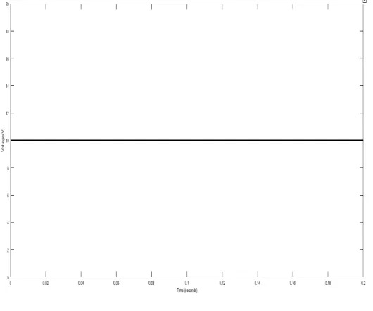
[image:5.612.176.441.264.485.2]three configurations are simulated with 70 % duty ratio at 50 kHz switching frequency. The proposed converters drive on regulated 10V DC supply with time constant of 0.04 as shown in Fig. 4.
Fig. 4 Regulated input supply
In MCCVLSI-XLL structures, capacitor C1 is charge up to 35.5V as shown in Fig. 5(a). The pulse output as shown in Fig. 5(b). The dc output voltage is 97.5V as shown in Fig. 5(c).The dc output current is 0.48A as shown in Fig. 5(e).The ac output voltage is 97.4V as shown in Fig. 5(d).The ac output current is 0.48A as shown in Fig. 5(e).
(d) Ac Output Voltage (e) Dc output Current (f) Ac output Voltage
Fig. 5 Simulation result of MCC-XLL structure converter outputs
In MCCVLSI-LLZ structures, capacitor C1 is charge up to 29.7V as shown in Fig. 6(a). The pulse output as shown in Fig. 6(b). The dc output voltage is 76.3V as shown in Fig. 6(c).The dc output current is 0.38A as shown in Fig. 6(e).The ac output voltage is 76.3V as shown in Fig. 6(d).The ac output current is 0.38A as shown in Fig. 6(f).
(a)Capacitor output voltage (b) Pulse Output (c) Dc Output Voltage
(d) Ac Output Voltage (e) Dc output Current (f) Ac output Voltage
Fig. 6 Simulation result of MCC-LLZ structure converter outputs
V. CONCLUSION
REFERENCES
[1] F. Blaabjerg, Y. Yang, K. Mam, X. Wang, “Power Electronics-The key Technology for Renewable Energy System Integration” Conf. Proc. Of 4th Intl. conf. on Renwable Energy Research and Application (IEEEICRERA’, Palermo, Italy, 2015..
[2] B. Baddipadiga, M. Ferdowsi, “A High-Voltage-Gain DC–DC Converter Based on Modified Dickson Charge Pump Voltage Multiplier”, IEEE Trans. on Power Electron., Vol. 32, No. 10, pp.7707-7715, Oct. 2017..
[3] M. Forouzesh, Y. Shen, K. Yari, Y. P.Siwakoti, F.Blaabjerg,”High- Efficiency High Step-Up DC–DC Converter With Dual Coupled Inductors for Grid-Connected Photovoltaic Systems”, IEEE Trans. On Power Electronics, Vol. 33, Issue 7, pp. 5967-5982, July 2018.
[4] L.Schmitz, D. C. Martins Roberto, F. Coelho, “Generalized High Step- Up DC-DC Boost-Based Converter With Gain Cell”, IEEE Trans. On Circuits and Systems, Vol. 64, No. 2, pp. 480-493, Feb. 2017.
[5] R. Wai, C. Lin, R. Duan, Y. Chang, “High-Efficiency DC-DC Converter With High Voltage Gain and Reduced Switch Stress”, IEEE Trans. on Industrial Electronics, Vol. 54, No. 1, pp 354-364, Feb. 2007.
[6] T. Sreekanth, N. Lakshminarasamma, M. Mishra, “Coupled inductorbased single-stage high gain DC–AC buck–boost inverter”, IET Power Electronics, Vol. 9, No. 8, pp. 1590–1599, Aug. 2016.
[7] Y. P. Siwakoti, F. Blaabjerg, P. C. Loh, “Quasi Y-source boost DC-DC converter”, Power Electronics and Applications (EPE'15 ECCEEurope), 2015 17th European Conference on, pp. 1-10, Sept. 2015.
[8] Y. P. Siwakoti, F. Blaabjerg, P. C. Loh,“Trans-inverse (Tx−1) high stepup DC-DC converter”, Power Engineering Conference (AUPEC), Australasian Universities, pp. 1-5, Sept.2015.
[9] L. M¨uller, J. Kimball, “High Gain DC–DC Converter Based on the Cockcroft–Walton Multiplier”, IEEE Trans. on Power Electronics, Vol. 31, No. 9, pp. 6405-6415, Sept. 2016.
[10] V. Prabhala, P. Fajri, V. Gouribhatla, B. Baddipadiga, M. Ferdowsi, “A DC–DC Converter With High Voltage Gain and Two Input Boost Stages”, IEEE Trans. on Power Electronics, Vol. 31, No. 6, pp. 4206- 4215, June 2016.
[11] F.L.Tofoli, P.Dênis de Castro, W.Josias de Paula, O.J.Demercil de Sousa, “Survey on non-isolated high-voltage step-up dc–dc topologies based on the boost converter”, IET Power Electron., pp. 1–14, July 2015.
[12] S.B. Mahajan, P. Sanjeevikumar, K.M. Pandav, R.M. Kulkarni, Sherke Vaibhav, “A Buck-Boost Current Converter Using Duality Concept and its DC Transformer Modelling” Lecture Notes in Electrical Engineering book- Springer, Advnaces in power system and energy management, Vol.436, pp.315-324, Dec-2016.
[13] B. Poorali, E. Adib, H. Farzanehfard, “ Soft-switching DC–DC Cuk converter operating in discontinuous-capacitor-voltage mode”, IET Power Electronics, Vol. 10, No. 13, pp 1679-1686, Nov. 2017.
[14] R. Moradpour, H. Ardi, A. Tavakoli, “ Design and Implementation of a New SEPIC-Based High Step-Up DC/DC Converter for Renewable Energy Applications”, IEEE Trans. on Ind.Electron., Vol. 65, No. 2, pp 1290-1297, Feb. 2018.