Implementation of Inter-Integrated Circuit (I2C)
Multiple Bus Controller on FPGA using VHDL
Mrs. Jaya Malviya1, Mr. Arif Mohammad2 1
M Tech (VLSI Design), Gyan Ganga Ins titute of Technology and Sciences, Jabalpur, Madhya Pradesh 2
Dept. of Electronics and Co mmunicat ions Gyan Ganga Ins titute of Technology and Sciences Jabalpur, Madhya Pradesh
Abstract: The Inter - Integrated C ircuit bus commonly called as I2C (I squared C) or I2C bus is a serial bus invented by Philips Semiconductors during early 80’s for interconnecting integrated circuits. In this paper, the design and implementation of a I2C Multiple Bus Controller (IICMB) core is presented.
Keywords: I2CMB, I2C Protocol, Avalon Memory mapped Interfaces, I2C Communication (key words)
I. INTRODUCTION
I2C bus was developed by P hilips Semiconductors during 1980’s for connecting computer peripherals together using a common protocol .This specification defines the architecture, hardware interface and parameterization options for the I2C Multiple Bus Controller (IICMB) core.
The IICMB core provides a low-speed, two-wire, bidirectional l serial bus interfaces compliant to industry standard I2C protocol. The key feature of the core is its ability to control several connected I2C buses effectively reducing complexity of system.
At any given moment the IICMB core works with a single I2C bus chosen from the range of connected buses (throughout this document such bus is called selected bus). When work with a particular selected bus is finished, user can switch to another one to continue configuring other peripherals. Every connected I2C bus is recognized by its number, or bus ID.
Note: The current version of the core supports master only functionality. S lave mode is under development. Proposed Features
1) Compatible with P hilips I2C standard 2) Works with up to 16 distinct I2C buses
3) Statically configurable system bus clock frequency
4) Statically configurable desired clock frequencies of I2C buses 5) Multi- master clock synchronization
6) Multi- master arbitration 7) Clock stretching
8) Digital filtering of SC L and SDA inputs
9) Standard (up to 100 kHz) and Fast (up to 400 kHz) mode operation 10) Connects as 8-bit slave on Wishbone bus
11) Connects as 32-bit slave on Avalon-MM bus
A. Architecture
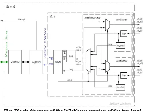
The core is provided with three examples of its top level (iicmb_m_wb.vhd, iicmb_m_av.vhd and iic_m_sq.vhd). Two of them are designed for Wishbone and Avalon-MM buses, while third version is a sequencer based one for deeply embedded applications without any system bus at all.
Fig. Block diagram of the Wishbone version of the top level
The wishbone.vhd module connects Wishbone b us to register block (regblock.vhd), which converts system bus accesses to byte- level commands of the Generic Interface. SCL and SDA inputs are digitally filtered to suppress unwanted spikes and to cope with long rising time of the I2C bus signals. The bus_state.vhd modules independently monitor busy states of all connected buses.
The conditioner_mux.vhd module, controlled by bus_id input, performs switching between connected I2C buses. The mbit.vhd and mbyte.vhd implement bit-level and byte- level FSMs, generating appropriate SCL and S DA waveforms in accordance to I2C Bus Specification
B. Operation
Some of the basic features on which have been implemented are as follows.
1) Implementation of IICMB core which provides low-speed, two-wire, bidirectional serial bus interfaces compliant to industr y standard I2C protocol.
2) “Manchester encoded UART” which enables running small peripherals with parasitic power derived from the TXD line, and allowing large clock differences typical of RC oscillators.
3) The key feature of the core is its ability to effectively reducing complexity of the system and control several connected I2C buses.
Signal Name I/O Description
Clk Inp ut Avalon-MM clock. M ain clock for the controller.
s_rst Inp ut Sy nchronous reset. Active high. waitrequest Outp ut Wait request.
readdata[31:0] Outp ut Data outp ut.
readdatavalid Outp ut Data validity indication. writedata[31:0] Inp ut Data inp ut.
Write Inp ut Indicates a write transfer. Read Inp ut Indicates a read transfer.
byteenable[3:0] Inp ut Enables sp ecific by te lane(s) durin g
Keeping in mind all the above specifications the key features of our design are
4) Works with up to 16 distinct I2C buses
8) Multi- master arbitration 9) Clock stretching
10) Digital filtering of SC L and SDA inputs
11) Standard (up to 100 kHz) and Fast (up to 400 kHz) mode operation 12) Example connection as 32-bit slave on Avalon-MM bus
C. Byte-level FSM
The byte-level FSM module (mbyte. vhd) communicates with upper level through so called Generic Interface. It accepts several byte- level commands listed in the Table 1 below.
After completion, each command is answered with an appropriate response. The main responsibility of the mbyte.vhd module is to translate byte- level commands to one or more commands for bit- level FSM (mbit.vhd).
Reception of a response is a mark of completion of the previously issued co mmand. It is an error to send next command before previous command is responded. S uch a command is ignored.
Byte- level commands
Byte- level responses Comma nd Code Para meter Description
Start “100” – If bus is not captured yet: issue Start Condition and
capture selected bus. If bus captured: issue Repeated Start Condition.
Stop “101” – Issue Stop Condition and free selected bus.
Read With Ack “010” – Receive a byte w ith acknow ledge.
Read With Nak “011” – Receive a byte w ith not- acknow ledge.
Write “001” Byte
of data
Transmit the byte given as a parameter.
Set Bus “110” Bus numbe
r (ID)
Connect to the specified bus (select bus).
Wait “000” Millise
conds
Do nothing for specified amount of time.
Respons e
Code Para mete
r
Description
Done “000” – Command completed.
Arb itrati on Lost
“010” – Arb itration lost. Selected bus is freed, FSMs are set to their idle states.
No Acknow ledge
“001” – Byte w ritten got no acknow ledge.
Byte “100” Byte
of data
Byte of data received.
The following diagram depicts the byte- level FS M
Byte- level FSM
D. Bit-level FSM
Bit-level commands and responses are hidden from the user of the core, but listed here for better understanding of how the two FSMs interact with each other.
Bit-level commands and responses have no parameters.
Level FSM
II. IMPLEMENTATION RESULTS
A. Setup 1
Top level module: iicmb_m_wb. vhd. Number of I2C buses (g_num_bus) = 1. System clock frequency (g_f_clk) = 100 MHz. I2C bus clock frequency (g_f_scl_0) = 100 kHz.
Device Utilization S ummary
Family Device Fmax Registe r Logics
Virtex-6 xc6vcx75t- 2-ff484
B. Setup 2
Top level module: iicmb_m_wb. vhd. Number of I2C buses (g_num_bus) = 16. System clock frequency (g_f_clk) = 100 MHz. I2C bus clock frequencies: g_f_scl_0 = 100 kHz, g_f_scl_1 = 120 kHz, g_f_scl_2 = 130 kHz, g_f_scl_3 = 200 kHz, g_f_scl_4 = 50 kHz, others = 30 kHz.
Family Device Fmax Registe r Logics
Virtex-6 xc6vcx75t- 2-ff484 325MHz 154 264LUT
III. HIERARCHY OF MODULES
Hierarchy of modules with Avalon-MM top level A. iicmb_pkg.vhd
B. iicmb_int_pkg.vhd C. iicmb_m_av.vhd
1) avalon_mm.vhd 2) regblock.vhd 3) iicmb_m.vhd a) mbyte.vhd b) mbit.vhd
c) conditioner_mux.vhd d) conditioner.vhd
i) filter.vhd ii) bus_state.vhd
Device Utilization S ummary
Slice Logic Utilization Used Available Utilization
Number of Slice R egisters 182 12,480 1%
Number used as Flip Flops 182
Number of Slice LUTs 318 12,480 2%
Number used as lo gic 307 12,480 2%
Number using O6 outp ut only 280
Number using O5 outp ut only 7
Number using O5 and O6 20
Number used as exclusiv e route-thru 11
Number of route-thrus 18
Number using O6 outp ut only 17
Number using O5 and O6 1
Number of occup ied Slices 147 3,120 4%
Number of LUT Flip Flop p airs used 375
Number with an unused Flip Flop 193 375 51%
Number with an unused LUT 57 375 15%
Number of fully used LUT -FF p airs 125 375 33%
Number of unique control sets 15
Number of slice r egister sites lost 22 12,480 1%
to control set restrictions
Number of bonded IOBs 59 172 34%
IOB Flip Flop s 1
Number of BUFG/BUFGCTRLs 1 32 3%
Number used as BUFGs 1
IV. CONCLUSION
In this project work, the multi- master facility of I2C protocol is implemented successfully. Address resolution is the major concern while using multiple masters in I2C bus. Arbitration procedure must be perfect for the bus to work properly when dual masters are present. A dual master I2C bus controller system with an EEP ROM 24CXX series as the slave devices has been developed for realizing both the read and write cycles of the I2C bus and tested. The design has got successfully implemented in Spartan 3A FPGA and the outputs are verified. Also DS1307 RTC is connected as the slave device and performed the WRITE and READ operations following I2C protocol. This design can be used in systems where multiple devices needs to be interconnected by ensuring with low complexity and efficient resource utilization.
REFERENCES
[1] I2C Bus Specification, P hilips Semico nductor, vers ion 2.1, Ja nuary 2000. [2] DS1307 64 x 8, Serial, I2C Real Time Clock , Maxim integrated, 2008.
[3] E. Allier, G. S icard, L. Fesquet, and M. Re na udin, “A new clas s o f async hro nous A/D converter s based o n time qua ntiza tio n,” in Proceed ings o f Inter nationa l S ymposium on Async hronous C ircuits a nd Syste ms, Ma y 2003, pp. 196–205..
[4] Prototyping o f Dua l Master I2C Bus Controller, Ana gha A , M. Mathuraka ni, Inte r nationa l Confere nce on Communication and S igna l Processing, April 6-8, 2016, India.
[5] Pro f. Ja i Kara n Singh et a l “Design a nd I mp le me nta tion o f I2C master controller on FPGA using VHDL,” IJ ET, Aug-Sep 2012.
[6] Raj Ka ma l, “Devices a nd Co mmunication Buses fo r De vice s Network,” in Embedded sy stem: Architecture programming and Design, S ha lini Jha Ed. New Delhi, I ndia : Tata McGra w-Hill Educatio n, 2008, pp.160- 165.
[7] I mp le me nta tion o f I2C Master Bus Controller on FPGA, Bolla m Es wari, N.Ponma ga l, K.Preethi, S.G.Sr eejee s h, Internatio na l conference o n Co mmunication a nd S igna l Processing, April 3-5, 2013, Ind ia
[8] I2C Hardwa re Master Ser ia l Inter face for As ync hro nous ADCs. Wojciech Andrysiewic z, Dariusz Ko´scielnik, Ma rek Mi´skowicz AGH University o f Scie nce a nd Technolo gy. 2015 IEEE.
[9] A.P.Godse, D. A.Godse, “Bus S ta ndard s,” in M icropro cessors and its Applications, 3rd Ed. Pune, I ndia : Technica l publications, 2008. [10] Syste ms with PIC Microcontroller s: Princ iples a nd Applicatio ns, 2 nd Ed. Burlinto n: Newne s, 2009, pp.307-327.
[11] Spartan-3A/3AN FPGA Starter Kit Board User Guide, Xilinx, versio n1.1, 2008.
[12] Vincent Himpe, “Histor ica l back ground o f I2C,” in Mastering the I2C Bus, Aachen, Germa ny: Elek tor Verla g publicatio ns, 2011.
[13] Interfacing of digital TPH sen sors with FPGA using I2C interface. Muha mmed Raees PC, Ana nd Lokapure, Sa ra f Ma ndar N, B.Satya na ra ya na. 2016 IEEE Bo mba y Section Symposium.
[14] BMP280 Digita l Pressure Se nsor Data sheet, Bosc h Se nsortec, October 15th, 2015. [15] AN10216-01 I2C Manual, P hilipsSemico nductor, Ma rch 2003.