warwick.ac.uk/lib-publications
Original citation:
Vesper, Malte, Koch, Dirk, Vipin, Kizheppatt and Fahmy, Suhaib A. (2016) JetStream : an
open-source high-performance PCI express 3 streaming library for to-host and
FPGA-to-FPGA communication. In: International Conference on Field-Programmable Logic and
Applications, Lausanne, Switzerland, 29 Aug - 2 Sep 2016. Published in: Proceedings of the
International Conference on Field-Programmable Logic and Applications
Permanent WRAP URL:
http://wrap.warwick.ac.uk/81284
Copyright and reuse:
The Warwick Research Archive Portal (WRAP) makes this work by researchers of the
University of Warwick available open access under the following conditions. Copyright ©
and all moral rights to the version of the paper presented here belong to the individual
author(s) and/or other copyright owners. To the extent reasonable and practicable the
material made available in WRAP has been checked for eligibility before being made
available.
Copies of full items can be used for personal research or study, educational, or not-for profit
purposes without prior permission or charge. Provided that the authors, title and full
bibliographic details are credited, a hyperlink and/or URL is given for the original metadata
page and the content is not changed in any way.
Publisher’s statement:
© 2016 IEEE. Personal use of this material is permitted. Permission from IEEE must be
obtained for all other uses, in any current or future media, including reprinting
/republishing this material for advertising or promotional purposes, creating new collective
works, for resale or redistribution to servers or lists, or reuse of any copyrighted component
of this work in other works.
A note on versions:
The version presented here may differ from the published version or, version of record, if
you wish to cite this item you are advised to consult the publisher’s version. Please see the
‘permanent WRAP url’ above for details on accessing the published version and note that
access may require a subscription.
JetStream: An Open-Source High-Performance
PCI Express 3 Streaming Library for FPGA-to-Host
and FPGA-to-FPGA Communication
Malte Vesper, Dirk Koch
School of Computer Science The University of Manchester [email protected]
Kizheppatt Vipin
Mahindra École Centrale [email protected]
Suhaib A. Fahmy
School of Engineering University of Warwick [email protected]
Abstract—Many FPGA-based accelerators are constrained by the available resources and multi-FPGA solutions can be necessary for building more capable systems. Available PCIe solutions provide only FPGA-to-Host communication. In this paper we present JetStream, an open-source1 modular PCIe 3 library, supporting not only fast FPGA-to-Host communication, but also allowing direct FPGA-to-FPGA communication which fully bypasses the memory subsystem. The direct mode saves memory bandwidth for multicast modes and permits to connect multiple FPGAs in various software defined topologies. We show the benefits of JetStream with a large FIR filter spanning four FPGA boards, achieving throughputs of up to 7.09 GB/s per link. Utilizing direct FPGA-to-FPGA transfers reduces the required memory bandwidth by up to 75%.
I. INTRODUCTION
Many FPGA-based accelerators need to communicate with other devices, either because the logic does not fit on a single FPGA (i.e. Catapult [2]) or since the data calls for pre- or post-processing for which another platform is better suited (e.g. a GPU in a heterogenous compute environment). PCI Express (PCIe) is a natural choice for linking FPGAs to other devices; it is prevalent, the first choice for PC extension cards, and many FPGA prototyping boards are designed to support PCIe at high speed. There are many applications (e.g., linear algebra, neural networks, and signal processing) that can substantially benefit from multi-FPGA solutions and commercial systems like Microsoft Catapult [2] and the MPC-X series from Max-eler [3] are designed for this scenario.
Nevertheless, the IP provided by FPGA vendors still re-quires complex additional logic to manage packets and a user-supplied driver before the PCIe connection can be actually used. There are several commercial and academic solutions available that provide drivers and wrap the vendor-supplied IP with stream interfaces.
All these solutions have chosen different trade-offs regard-ing speed, size and feature set as revealed in Section II. While we include commercial solutions for completeness, these are not suited for many projects due to their monetary cost and limited adaptability for fine tuning as they are not open source.
1Available at https://maltevesper.github.io/JetStream/
To overcome this, we present JetStream [1], a PCIe 3 solution, which adds direct FPGA-to-FPGA communication, a feature we have not found in any other solution. In addition, we incorporated several performance tweaks commonly not considered. Furthermore, our solution supports PCIe 3 on an 8-lane link. Currently, ffLink is the only other open-source solution we have found that supports PCIe 3 on 8 lanes despite most FPGA boards supporting 8 lanes. All other PCIe 3 solutions support only 4 lanes, limiting them to half the speed. A distinctive feature of JetStream is support for direct FPGA-to-FPGA transfers. We use direct FPGA-FPGA-to-FPGA transfers to implement broadcasts, allowing us to reduce the required memory bandwidth by up to 75 %.
JetStream allows to build Multi-FPGA solutions that can be beneficial since large capacity FPGAs can cost over-proportional more money per available resources. Another rea-son for using multiple smaller FPGAs can be if this improves the aggregated capacity and/or throughput of the memory over all boards. Finally, there could be power constraints that may prevent using large capacity FPGAs. For example, when not considering optional power connectors, an x8 PCIe half height card is bound to 10W and up to 25W for a full height card in high power mode, according to the PCIe specification [4].
The rest of the paper is organized as follows: Section II gives an overview of related work and other available so-lutions, Section III gives a brief introduction to PCIe fun-damentals. Afterwards we present the internal hardware in Section IV and follow with a description of the hard- and software-API provided (Section V). Performance results are collected in Section VI and Section VIII concludes the paper.
II. AVAILABLEPCIE SOLUTIONS
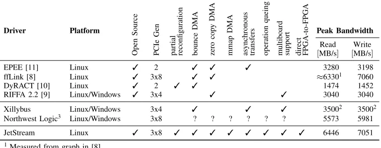
Driver Platform Peak Bandwidth
Read
[MB/s]
Write
[MB/s]
EPEE [11] Linux 3 2 3 3 3 3280 3198
ffLink [8] Linux 3 3x8 3 3 ≈63301 7060
DyRACT [10] Linux 3 2 3 3 1474 1452
RIFFA 2.2 [9] Linux/Windows 3 3x4 3 3 3040 3040
Xillybus Linux/Windows 3x4 3 3 3 35002 35002
Northwest Logic3 Linux/Windows 3x8 ? ? ? ? ? ? 5573 5981
JetStream Linux 3 3x8 3 3 3 3 3 3 3 3 6446 7051
1Measured from graph in [8]. 2According to estimate limit in [6].
[image:3.612.116.500.58.207.2]3Driver is closed source, thus analysis is not possible.
TABLE I: FPGA PCIe framework comparison.
Open
Source
PCIe
Gen
partial reconfiguration bounce
DMA
zero
cop
y
DMA
mmap
DMA
asynchronous transfers operation
queing
multiboard support direct FPGA-to-FPGA
coherent memory between the FPGA and a host. Its advantage is that no software stack is involved in transfers, hence, reducing latency. However, this requires a special interface at the processor on the host side, currently only found in IBM’s Power8 processors. For this reason, we will not consider CAPI any further.
On the academic side ffLink [8] and RIFFA 2.2 [9] support third generation PCIe. While ffLink is built from a chain of Xilinx-supplied AXI IP-blocks and supports 8 lanes, RIFFA provides software APIs for several languages and a windows driver. However, RIFFA only supports 4 lanes.
DyRACT [10], EPEE [11], FlexWAFE [12], Speedy [13] as well as the implementation of Kavianipour et al. [14], are PCIe solutions supporting generation 2. Kavianipour is slow, peaking at 52 % of the theoretical bandwidth. EPEE focuses on the idea of a PCIe library; besides streaming interfaces, it allows for a user register file and user generated interrupts. DyRACT is a stripped-down version of the system level FPGA driver presented in [15]. Both systems focus on the idea to provide partial reconfiguration over PCIe, allowing the user to swap modules during runtime and to set the clock frequency for the user logic. FlexWAFE is a framework to stitch image processing nodes together for stream processing. It uses PCIe to configure the FPGAs (not partially) and to stream the data through the FPGAs. It uses multiple FPGAs on one board: one is used as the PCIe router that is not reconfigured, and the rest as processing FPGAs that are linked to the PCIe router FPGA by an FPGA-to-FPGA connect.
Table I gives an overview over the features and performance of the different solutions. The last row of the table lists the features of JetStream.
III. PCI EXPRESS FUNDAMENTALS
The PCIe 3 protocol stack [4] is organized in three layers: transaction layer, data link layer and physical layer. The user application generates packets on the transaction layer consist-ing of a 12 B/16 B header (the latter is for 64-bit addresses), the payload of 0...4096 B, and an optional 4 B ECRC checksum.
STP
4 B
Header
12. . .16 B
Payload
0. . .4096 B
[ECRC]
0. . .4 B
LCRC
4 B
Fig. 1: PCIe Memory Packet.
The data link layer adds a 4 B LCRC checksum and handles flow control with ack messages to confirm successful transfers. The link CRC (LCRC), secures the link layer. However, since the LCRC is computed over parts of the header that change during routing, it is recomputed in switches, thus potentially masking errors introduced in the switch. The end-to-end CRC (ECRC) on the other hand is computed over the invariant parts of the header and the payload. It adds another (optional) layer of data integrity control.
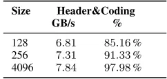
The link layer also provides a credit system. The credit system keeps track of the buffer-space on the receiving end. The physical layer adds a frame around each packet and applies 128 b/130 b coding to it (which is 18 % more efficient than the 8 b/10 b coding used by PCIe 2). The frame is 4 B for transaction layer packets (TLP), and 2 B for data link layer packets (DLLP) used for flow control. In total the minimum overhead per packet of 20 B/24 B is composed of a 4 B frame, a 12 B/16 B header and a 4 B LCRC checksum as shown in Figure 1.
After the packets have been assembled, they are transferred over the link. A link is composed of 1. . .32 lanes, each lane consists of two differential pairs, one to and another one from the endpoint. Since PCIe 3 operates at 8 GT/s2, an 8 lane
PCIe 3 (PCIe 3x8) link provides a theoretical bandwidth of 8 GBs.
Not accounting for flow control and assuming a maximal payload of 4096 B and a 12 B header this results in a theo-retical throughput of 7.84 GB/s (97.98 %) for a 8 lane link. However, in practice the PCIe root complexes3 found on
2Gigatransfers per second
3Toplevel node in the PCIe hierarchy, interfaces to the host CPU and main
Request
Engine arbiter
Channel 3 Channel 2 Channel 1
Registerfile Completion
Engine
Xilinx PCIe
core
User Module 1 User Module 2 User Module 3
ICAP User register file
[image:4.612.98.509.50.199.2]Userlogic
Fig. 2: System overview. Note that user modules can utilize channels as needed. The green dotted arrow represents a sink channel.
Size Header&Coding
GB/s %
128 6.81 85.16% 256 7.31 91.33% 4096 7.84 97.98%
TABLE II: Theoretical throughput.
consumer CPUs do not allow for unlimited credit, making flow control mandatory and limit the maximum payload to 128 B or 256 B. Table II gives an overview of the relevant theoretical limits. For further details on estimating theoretical throughput we refer to [16]. To understand possible discrepancies between theoretical and practical performance see [17].
PCIe differentiates between two transaction types: posted and non-posted transactions. Posted transactions are transac-tions that are considered complete by the sender by the time the last byte is dispatched, i.e. a memory write transaction. Non-posted transactions on the other hand warrant a reply, i.e. memory read transactions. The transaction does not complete after the request header has been sent, but only when the requested data arrives (or when the transaction times out).
IV. JETSTREAM HARDWARE
In this section we present the JetStream hardware imple-mentation, starting with the system overview in Figure 2 and explaining details for separate modules and our performance tweaks towards the end.
The Xilinx IP core [18], around which our design is built, has four AXI interfaces for data transfers: CompleterComple-tion, CompleterRequest, RequesterCompleCompleterComple-tion, and Requester-Request. The interfaces form two pairs: the Completer*-interfaces handle transactions initiated by the host, while the Requester*-pair is used for transactions initiated by the FPGA. The Completer-andRequesterEngine are connected to the corresponding interface pair. The engines create/decode the headers and realign the data, as it arrives DWORD-aligned and we return it address-aligned on a 256 bit interface.
The register file, into which the host programs the address and size for DMA transfers, is connected to the
Completion-Engine. Since the number and kind of channels provided is parameterizable, we have registers to reflect this information so that the driver can autoconfigure itself. Furthermore, we have a channel register group for every channel. This group contains FIFOs that serve as size- and address-registers al-lowing the host to issue multiple commands as well as a channel control register. The completion counter, which tells the host how many operations have completed, is actually a part of the register file itself. This way, multiple counters can be combined into one register, requiring the host driver to read less registers when checking for command completion. While JetStream does not give the user direct access to the register file (ensuring that single modules cannot break the system) we provide a register file interface that maps read-and write-addresses in a configurable range to the user logic. This allows users to implement their own registers. However, this user register file is global. If per module register files are desired, it is the user’s responsibility to divide the user address space accordingly.
The arbiters are responsible for picking valid commands and arbitrating between them. We implemented one arbiter for send-commands and another arbiter for receive-commands, as PCIe is a full-duplex system. Each arbiter is split into two parts, thecommand logicand thearbitration logic. The former determines the size of potential transfers by looking at the commands stored in the register file and the available data. It also updates the transfer’s start address and remaining size, if it has to be split into multiple transfers, due to PCIe’s payload or request size limitations [4]. The command logic also manages the multiplexing of data between the user modules and the request engine. It generates a vector indicating which channels currently have valid requests available which is fed into the arbitration module. The arbitration module contains the arbitration logic, which returns a one-hot encoded vector, indicating which channel is arbitrated. By default, this is a priority encoder, but it can be swapped easily by the user since it is implemented in a separate module.
[image:4.612.113.234.248.305.2]commands to interfere with each other. This is resolved by the requester which tries to keep a minimum number of requests in flight, to ensure that both directions of the link are fully utilized.
The user modules can be filled with custom logic, given that they are able to receive/create at least min(MAX_Payload,MAX_command_size)data at wire speed and announce the amount they can currently provide/receive. This policy prevents slow modules from blocking the entire system by clogging a central buffer and allows for further optimization. Firstly, if one implements a module that requires data in a RAM anyway, there is no need to have a buffer-FIFO in between. Secondly, modules with one input and one output, which are able to process data at wire-speed, only require a buffer at one end.
To ease the implementation of user logic, we provide parameterizable buffer-FIFOs for the latter case, as well as a buffer for the send- and another FIFO for the receive-side. For convenience we also provide a send- and receive-buffer for the common case of modules which employ one input and one output stream. The FIFOs of our buffers provide AXI stream interfaces [19] to the user, while the arbiter has a data, valid, and amount interface. The arbiter interface handles back pressure on a per transfer basis via the amount signal.
While the general purpose channels are managed by the FPGA to provide DMA access from the CPU’s view and thus go through the RequestEngine, sink channels are connected directly to the CompletionEngine. The main purpose of sink channels is to serve as endpoints for direct FPGA-to-FPGA transfers. In case of such a transfer, one FPGA will be the master controlling the transfer and the other FPGA will inevitably receive the data on its completer interface.
Even though, our implementation does not limit the number of channels, a larger arbiter might not meet timing. This can be circumvented by hierarchical arbitration, at the expense of latency.
To make our library universal we allow master mod-ules which enable user logic to generate send- or receive-commands. Master modules are connected to the arbiter in-stead of a channel register group and provide the size and address of the next command. This can be used to create DMA-engines, or to implement direct FPGA-to-FPGA trans-fers without host intervention.
While the arbiter generates interrupts to signal command completions automatically, we provide 31 user interrupts for custom signaling.
In summary, the user can configure the number of channels and their types by providing a list of channel types. Providing this list is sufficient to start implementing user logic. Apart from instantiating an appropriate buffer module, no further work is required. Interrupts can be triggered by the user logic by asserting bit lines in a vector and a global register file can be created easily by filling in a provided template.
The arbitration logic can be adjusted by generating a one hot encoded signal from a vector of available channels. Additional predefined modules are available that can either be used
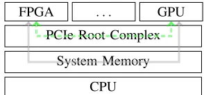
CPU System Memory PCIe Root Complex
[image:5.612.361.508.49.118.2]FPGA . . . GPU
Fig. 3: Direct transfer (green, dashed) between two PCIe devices vs indirect DMA transfer (gray).
directly or used as a template. The predefined modules include a partial reconfigurator, which allows partial reconfiguration over PCIe through the internal configuration access port (CAPI).
A. Direct FPGA-to-FPGA communication
Back pressure for transfers between host and FPGA is handled by the FPGA. When the driver programs a command into the register file, it already set aside sufficient memory on the host side. The arbiter in the FPGA then checks for each transfer that it has enough data available before starting the transfer of each packet. However, for FPGA-to-FPGA transfers, there are limited buffers on both ends. Since we do not want to block the PCIe core, which would stall all other channels as well, we cannot rely on the PCIe credit system. Therefore, one of the two communicating FPGAs needs to tell the other FPGA when sufficient buffer space is available.
JetStream uses a mechanism where the target FPGA sends requests for data to the source whenever it has sufficient buffer space available. The requests are sent to the source-FPGA, where a master module generates an according send-command. The arbiter then ensures that the send is not started before sufficient data is available. The target receives the data via its completer-interfaces. The data is routed to the correct sink channel based on the destination memory address. We chose to implement FPGA-to-FPGA transfers this way since it requires only an extension of the CompleterRequest side (the package arrives as a request from the source).
Figure 3 highlights the advantages of direct point-to-point transfers. While a DMA transfer (gray arrow) causes an addi-tional memory write and an addiaddi-tional read, a direct transfer bypasses the main memory thus saving memory bandwidth. Furthermore, PCIe is not a bus but rather a fully switched point-to-point network. On a normal mainboard, all PCIe links can be active at the same time.
To implement broadcasts we daisy chain the data from one FPGA to the next. This reduces the required memory bandwidth tremendously as we will show in Section VI.
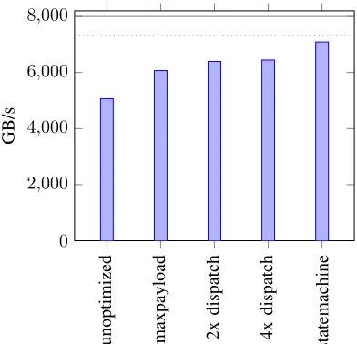
B. Performance optimizations
unoptimized maxpayload 2x
dispatch
4x
dispatch
statemachine
0 2,000 4,000 6,000 8,000
[image:6.612.55.251.49.238.2]GB/s
Fig. 4: Speed gain by successively adding optimizations.
since the request size rises from 128 B to 512 B, reducing the number of requests needed by a factor of four. If the system does not have enough credits, the system has to wait for credits before it can dispatch further requests. This can lead to gaps in the data stream, resulting in a 300 % increase for receive. However, since the remaining optimizations had little effect on receive operations, they are not shown here.
Our dispatch queues, which allow to have multiple requests in flight, increased performance by another 8 %. With only one request in flight there is always a small gap between successive requests, since the next request can’t be dispatched to the FPGA before the interrupt is handled by the host. However, as the graph shows, there is little benefit in deeper dispatch queues if operations can be orchestrated in sufficiently large chunks.
The last optimization is related to the state machine. The Xilinx PCIe core requires a 256 bit interface running at 250 MHz when using 8 PCIe lanes. Consequently the data can be supplied at 8 GB/s. A 256 B packet needs 9 cycles to transfer (8 data beats and half a beat for the header), which means that each cycle lost per packet reduces throughput by 11 %. By modifying our state machine to dispatch the next packet in the same cycle as the previous one completes, we were able to achieve optimal performance. We found that our fastest measured send rate was 7.09 GB s which is below the theoretical 7.31 GB/s reported in Table II. The cause for this stems from the used Xilinx IP core. Because the core can not accept multiple packets on the RequesterRequest interface, it needs 9 cycles per packet. At 250 M cycles, this results in 27.7M 256 B-packets or7.1GB/s.
V. JETSTREAMAPI
The JetStream C++ API provides three transfer modes as depicted in Figure 5. The modes differ in their speed and complexity: zero copy DMA, single buffering and double buffering. The modes differ in how the driver ensures that the data ends up in a DRAM area that is accessible by PCIe.
driver PCIe
userspace kernel space FPGA
swap
swap
Fig. 5: Different DMA modes. From top to bottom: zero copy DMA, single buffering, and double buffering.
The buffering modes copy the data from the user memory space into a bounce buffer allocated by the driver. The FPGA then operates on this buffer for host-to-FPGA transfers. The direction and order of the copy operations is reversed for transfers from the FPGA to the host. Whereas single buffering works with only one buffer and has to wait for the FPGA to finish before copying data between the user and the buffer, double buffering employs two buffers. While the FPGA copies data into/out of one buffer, the driver can already transfer data between the user program and the other buffer.
The buffering methods imply an extra copy of the data; the data is copied between the programs memory and the buffer. Zero copy DMA on the other hand supplies the program with memory that is FPGA accessible (i.e. a pinned down memory region in the address space accessible by the FPGA). This way it is unnecessary to copy the data around in main memory reducing data movement to a minimum.
The C++-API provided by JetStream is built around four objects: FPGA, Buffer, Channel and Operation. FPGA is the only object that can be constructed directly by the user, Channel- andBuffer-objects are subsequently obtained from theFPGA-object. For brevity, only the send case is described, receiving data works analogous.
Every program using JetStream will start with the creation of an FPGA-object, either explicitly requesting an FPGA by inspecting the list of FPGAs available (FPGA::list()) or implicitly grabbing one that is currently not used. For bounce buffer transfers, all that is needed is FPGA().bufferedSend(channelId, start*, size,
[image:6.612.312.563.52.229.2]Buffer- orOperation-objects. In each case these functions check if all operations on the object have finished. For in-stance, FPGA.finsihed() checks if there are any transfers outstanding for the FPGA, while Operation.finished() simply checks if a particular operation has completed.
Apart from Operation objects, all other objects wait() when they are destroyed. For Channel and Buffer objects this synchronization can be suppressed by calling noSync(). The FPGA object will ensure that the buffers persist until all transfers are completed before the program terminates.
For zero copy transfers, the mechanism is only slightly different. The first step is to allocate zero copy memory by calling FPGA.malloc() which returns a buffer. After filling the memory belonging to the buffer with data, the buffer is passed either to theFPGA’ssend()function or transferred by callingsend()on theBuffer. This brings us to the difference betweenChannel.send,Buffer.sendandFPGA.send. As a matter of fact, all three methods perform the same operation, however they need different parameters since their objects contain different information. While FPGA.send needs to know the channel and buffer, Channel.send only requires the buffer to operate on. WhileBuffer.senddoes not require any particular parameters for convenience, it should be stated that a buffer is independent from an FPGA or channel. Thus, one can specify these in Buffer.send() to send a buffer to a different FPGA. The sync* versions of the transfer functions are blocking, while the other transfer functions execute asynchronously.
The JetStream driver handles multithreading, ensuring that it is save to operate on the same FPGA from different threads or processes. While this has to be requested by creating the FPGA object with the exclusive flag set to false, it also brings one problem: Consider a filter that should be shared. To share this accelerator, one has to en-sure that the result arrives back at the source of the cor-responding input. To ensure this we can either lock() the FPGA and issue a corresponding send/receive pair, or make use of FPGA.transaction. FPGA.transaction returns a Transaction-object that works likestd::lock_guard, i.e. access to the FPGA is exclusive while the object exists.
The JetStream API also provides functions to access the register file (readRegister(), writeRegister()), and to handle user generated interrupts. The user can either check whether an interrupt has occurred in the past, block until one occurs, or register an asynchronous callback.
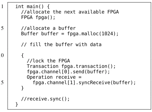
A. A FIR Filter with JetStream
The following shows how a FIR filter can be implemented. We assume that the filter itself is already implemented; the next step is to connect the FIR filter to JetStream. The FIR filter has one input channel and one output channel. Therefore, we set the CHANNELS parameter in JetStream to 2, and specify the CHANNEL_TYPES as {CHANNEL::INPUT, CHANNEL::OUTPUT}. Next we create a module to be instanti-ated by JetStream. As ports we specify the signals for one send channel and one receive channel. To fulfill JetStreams buffer
1 int main() {
//allocate the next available FPGA FPGA fpga();
5 //allocate a buffer
Buffer buffer = fpga.malloc(1024);
// fill the buffer with data
10 {
//lock the FPGA
Transaction fpga.transaction(); fpga.channel[0].send(buffer); Operation receive =
15 fpga.channel[1].syncReceive(buffer);
}
[image:7.612.312.568.47.235.2]//receive.sync(); }
Fig. 6: FIR code example.
requirement, we instantiate the two way buffer provided by JetStream. This creates a buffer for the input and onther one for the output channel and connects the FIR filter to these buffers.
We will now introduce how a user program can access the FIR accelerator module running on the FPGA, as shown in Figure 6. As shown in Section V, the API is built around the FPGA-object. We start by accessing the first available FPGA in the system (line 3), next we allocate a zero copy buffer (line 6). After the buffer is filled, we send the data to the FPGA (line 13) and setup the response from the filter (line 14). To ensure that no other thread reads our data, by issuing a read before we can, we lock the FPGA (line 12) while setting up the transfers. This gives us exclusive access to the FPGA and ensures that no other process can queue an operation in between our send and receive. As we specified the INPUT channel first in the channel list, it will have the channel ID 0. Therefore, we send our data to channel 0 and receive data from channel 1. Since there won’t be enough data to receive before the send operation completes, it is enough if we synchronize on the receive operation. We can either synchronize on the spot usingsyncReceive, or let the operation run asynchronously (usingreceive) to perform other work before synchronizing (indicated in line 18). Accounting for the main boilerplate code, sending and receiving data can be done in only six lines of code.
VI. PERFORMANCEHOST TOBOARDS
For our experiments, reported in this section, we used the Xilinx VC709 development board in a host PC featuring an Intel Core i7-5930K running at 3.5 GHz and 1-4 memory channels with 64 GB of DDR4-RAM at 2133 MHz. This CPU provides 40 PCIe 3 lanes, and allows for up to four 8-lane links4.
JetStream Northwest Riffa 2.2 Xillybus 0
2 4 6
0 200 400 600
·104
Luts/FF BRAM
7k
0k
57k
7k
17 16
173
12
LUT LUTRAM FF BRAM
8.6k
69.5k
49.6k
[image:8.612.50.301.51.246.2]7.1k
Fig. 7: Resource usage comparison.
JetStream Northwest Riffa 2.2 Xillybus
LUT 8571 69500 49565 7053
LUTRAM 392 0 1552 377
FF 6955 0 57147 6634
BRAM 17 16 173 12
TABLE III: Resource usage comparison.
We tested three modes supported by our driver, bounce-buffering, double-buffering and zero copy DMA, with one to four boards.
The resource usage is shown in Figure 7 and Table III. As can be seen, JetStream is very close to the smallest reference solution (which is Xillybus), but provides almost double the throughput of that solution (see Table I). The fine granularity which allows the user to decide buffer sizes for each channel helps in saving resources.
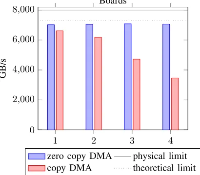
Figure 8 shows the bandwidth achieved per board, for the case that multiple boards are sending at the same time. Figure 9 shows the same for multiple FPGAs receiving at the same time. In both figures it can be seen that the chosen transfer type affects the result. While the per board bandwidth stays constant for zero copy transfers, it drops significantly for bounce buffer transfers after the second FPGA. This is caused by the twofold increase in memory access compared to zero copy DMA. For bounce buffer transfers the data has to be read from the user space and copied to the DMA buffer before the FPGA can actually read it. This requires three times the memory bandwidth of the actual throughput. At 6.4 GB/s write speed this means 38.4 GB/s for two FPGAs and 57.2 GB/s for three FPGAs (close to the theoretical maximum of 60 GB/s which our system provides). While zero copy DMA is 3 fold more throughput efficient, we would hit the available host PC memory bandwidth with four FPGA boards that send and receive simultaneously. Even though, receive starts out significantly faster at 6.85 GB/s it declines considerably faster since it is limited to the same maximum main memory
1 2 3 4
0 2,000 4,000 6,000
8,000 Boards
GB/s
[image:8.612.319.526.55.235.2]zero copy DMA physical limit copy DMA theoretical limit
Fig. 8: Send bandwidth per board for one to four FPGAs.
1 2 3 4
0 2,000 4,000 6,000 8,000
Boards
GB/s
[image:8.612.320.525.276.456.2]zero copy DMA physical limit copy DMA theoretical limit
Fig. 9: Receive bandwidth per board for one to four FPGAs.
bandwidth.
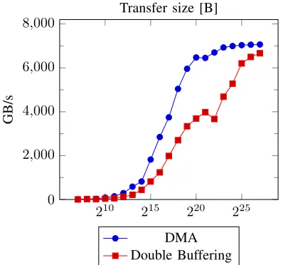
Figure 10 shows the relation between transfer size and speed. The speed seems to increase since larger transfers offset the initial time of issuing the first command to the FPGA better. Another explanation could be measuring inaccuracies, since we did not offset for the time of the measuring code.
VII. PERFORMANCEBOARD TOBOARD
To show the performance benefits of direct FPGA-to-FPGA transfers we implemented a large FIR filter. The FIR filter is so large that it does not fit into a single FPGA board. Therefore, we split the logic across four FPGAs and linked them using JetStream. We implemented two variants: in the first variant, the host PC supplies all the data to the FPGAs. In the second variant the host PC only sends data to the first FPGA which then daisy chains it to the next. The last FPGA in the daisy chain returns the data to the host.
[image:8.612.68.282.281.335.2]210 215 220 225
0 2,000 4,000 6,000 8,000
Transfer size [B]
GB/s
[image:9.612.316.559.49.128.2]DMA Double Buffering
Fig. 10: Send bandwidth vs. transfer size.
Function
Stream result [GB/s]
FPGAs
0 1 2 3 4
Copy 30.593 28.120 26.200 24.087 21.686
Scale 30.529 28.281 26.417 24.182 22.730
Add 33.499 31.740 29.890 28.057 26.234
[image:9.612.54.253.52.238.2]Triad 33.461 31.200 29.650 27.341 25.093
TABLE IV: Stream results with the host sending data to each FPGA.
transfers. As these transfers also access the memory, they re-duce the bandwidth available to the benchmark, thus reducing performance as more FPGAs are transferring data. Since direct FPGA-to-FPGA transfers do not go through the host memory, they should have no impact on the benchmark.
We ran the benchmark Stream [20] with 640 million ele-ments on 12 cores to measure the memory bandwidth on the host. To show the scaling, we varied the number of FPGAs involved in the FIR filter. As a baseline, we measured the system memory bandwidth while the system was idle apart from Stream. Table IV shows Stream results for the different configurations where the host supplies the data to each FPGA and Table V shows the results of the benchmark when direct FPGA-to-FPGA transfers are used.
Interestingly, we found that the DMA speed barely suffered from the running benchmark, although this might be caused by the fact that we send chunks of 1 GB and have timing code in between chunk transfers. This leaves gaps where the FPGAs are idle. Table V shows a slight performance drop even for direct FPGA-to-FPGA transfers compared to no active FPGAs. This is because we have to send the data from the host to the first FPGA.
VIII. CONCLUSIONS
Integrating FPGAs through PCIe is an ideal solution for many acceleration solutions. PCIe is widely available through various hardware platforms, it provides high throughput, and
Function
Stream result [GB/s]
FPGAs
0 1 2 3 4
Copy 30.593 28.120 28.215 29.040 28.761
Scale 30.529 28.281 28.151 28.645 29.217
Add 33.499 31.740 31.756 30.057 29.463
[image:9.612.55.295.269.348.2]Triad 33.461 31.200 29.650 31.341 30.953
TABLE V: Stream results with the FPGAs using direct FPGA-to-FPGA transfers.
PCIe does not occupy or need a CPU socket on a motherboard. Unfortunately, the FPGA vendors often provide only very rudimentary PCI support with only very limited features and with poor performance.
In this paper we present the JetStream PCIe infrastructure consisting of a PCIe core around the Xilinx vendor core, a Linux driver, and application examples. JetStream does not only provide high throughput (close to the theoretical maxi-mum) but it also features a rich API that supports direct FPGA-to-FPGA communication through PCIe without involving the memory subsystem of the host PC. This distinct mode allows connecting FPGAs together in arbitrary topologies that are fully software definable. Such multi FPGA solutions provide new opportunities for performance scaling, cost reduction, fault tolerance, and energy management in larger compute servers.
JetStream is open-source under GNU General Public Li-cense (GPL) and was developed and tested for the popular VC709 and the NetFPGA SUME Virtex-7 boards running Linux kernel version 4.35. JetStream works with the Vivado
tool suite from Xilinx and user modules can be easily inte-grated using standard AXI interfaces. JetStream is available at [1].
For future work, we aim at successively testing further boards and at providing corresponding reference projects. We intend to stimulate a wider usage of FPGAs as compute accelerators with this.
While we have not ported JetStream to Altera devices yet, we are very confident that JetStream can be easily ported. Xilinx provides two pairs of send and receive interfaces (one for host- and one for FPGA-initiated transfers, see Section IV), while Altera provides only one interface that is shared for host-and FPGA-initiated transfers [21]. This requires to combine the Completer- and the RequesterEngine. RIFFA [9] is a PCIe solution that has been ported to Xilinx and to Altera FPGAs, demonstrating the feasibility of a port.
ACKNOWLEDGMENT
This work is kindly supported by the project Reconfig-urable Tera Stream Computing funded by the Defence Sci-ence and Technology Laboratory, UK under grant DSTLX-10000092266.
REFERENCES
[1] M. Vesper, “JetStream GitHub page,” 2016. [Online]. Available: https://maltevesper.github.io/JetStream/
[2] K. Ovtcharov, O. Ruwase, J.-Y. Kim, J. Fowers, K. Strauss, and E. S. Chung, “Accelerating deep convolutional neural networks using specialized hardware,”Microsoft Research Whitepaper, vol. 2, 2015. [3] Maxeler Technologiesm, “MPC-X Series,” 2010,
https://www.maxeler.com/products/mpc-xseries/ accessed 28.03.2016.
[4] PCI-SIG,PCI Express Base Specification, Revision 3.0, PCI-SIG Std., 2010.
[5] N. Logic,IP Core Size & Speed (Xilinx FPGAs) v4.56, Northwest Logic, 2016.
[6] Xillibus,IP core product brief v1.8, Xillibus, Jan 2016.
[7] J. Stuecheli, B. Blaner, C. Johns, and M. Siegel, “Capi: A coherent accel-erator processor interface,”IBM Journal of Research and Development, vol. 59, no. 1, 2015.
[8] D. de la Chevallerie, J. Korinth, and A. Koch, “ffLink: A Lightweight High-Performance Open-Source PCI Express Gen3 Interface for Recon-figurable Accelerators,” inInternational Symposium on Highly Efficient
Accelerators and Reconfigurable Technologies (HEART), 2015.
[9] M. Jacobsen and R. Kastner, “RIFFA 2.0: A reusable integration framework for FPGA accelerators,” inInternational Conference on Field
Programmable Logic and Applications (FPL), 2013.
[10] K. Vipin and S. A. Fahmy, “DyRACT: A partial reconfiguration enabled accelerator and test platform,” in International Conference on Field
Programmable Logic and Applications (FPL), Sept 2014.
[11] J. Gong, T. Wang, J. Chen, H. Wu, F. Ye, S. Lu, and J. Cong, “An efficient and flexible host-FPGA PCIe communication library,” in In-ternational Conference on Field Programmable Logic and Applications
(FPL), 2014, pp. 1–6.
[12] A. d. C. Lucas, S. Heithecker, and R. Ernst, “FlexWAFE-a high-end real-time stream processing library for FPGAs,” inDesign Automation
Conference (DAC), 2007.
[13] R. Bittner, “Speedy bus mastering PCI express,” inInternational
Con-ference on Field Programmable Logic and Applications (FPL), 2012.
[14] H. Kavianipour, S. Muschter, and C. Bohm, “High performance FPGA-based DMA interface for PCIe,”IEEE Transactions on Nuclear Science, vol. 61, no. 2, 2014.
[15] K. Vipin, S. Shreejith, D. Gunasekera, S. A. Fahmy, and N. Kapre, “System-level FPGA device driver with high-level synthesis support,”
inInternational Conference on Field-Programmable Technology (FPT),
2013, pp. 128–135.
[16] A. Goldhammer and J. Ayer Jr, “Understanding performance of PCI express systems,”Xilinx WP350, Sept, vol. 4, 2008.
[17] R. Scherzinger, “Avoiding PCI Express link performance surprises,” 2006.
[18] Xilinx, Virtex-7 FPGA Gen3 Integrated Block for PCI Express v4.1, Xilinx, Sep 2015.
[19] Arm, “AMBAR 4 AXI4-Stream protocol specification,” Mar. 2010. [Online]. Available: http://infocenter.arm.com/help/ index.jsp?topic=/com.arm.doc.ihi0051a/index.html
[20] J. D. McCalpin, “STREAM: Sustainable Memory Bandwidth in High Performance Computers,” University of Virginia, Charlottesville, Virginia, Tech. Rep., 1991-2007. [Online]. Available: http://www.cs.virginia.edu/stream/