1
Faculty of Electrical Engineering,
Mathematics & Computer Science
OPTIMIZING FPGA DESIGNS
FOR MAXIMUM THROUGHPUT
USING RAPIDWRIGHT
Timon Kruiper B.Sc. Thesis
July 2019
Abstract
Nowadays the number of resources inside a field-programmable gate array (FPGA) are rapidly increasing. This opens up new research fields, because most designs wont use all the resources a FPGA has to offer. These extra resources can be used for several appli-cations, e.g. increasing security or improving throughput.
This research looks into the possibility to use the extra resources to increase throughput of FPGA designs. Throughput in a FPGA design goes hand in hand with the frequency at which the FPGA is running, being able to run the FPGA at a higher frequency results in a higher throughput. The limiting factor of the maximum frequency is the combinational logic and routing delays. By adding registers in between the logic these delays are reduced, which in turn increases the maximum frequency and thus increases the throughput. This method is called pipelining.
In this thesis an automatic approach to add pipeline stages is developed, instead of manually adapting the design. The Java tool RapidWright is used which allows for editing the netlist and is a perfect tool to do CAD for FPGAs. The algorithm is tested on several designs and it is shown that it does indeed improves the maximum frequency of FPGA designs up to 35% depending on the amount of latency that is desirable. For future research it should be looked into how RapidWright can place or route a design to further increase the throughput.
Contents
Abstract iii
1 Introduction 1
2 Background 3
2.1 FPGA Architecture . . . 3
2.1.1 Configurable Logic Blocks . . . 3
2.1.2 Block RAM . . . 5
2.1.3 Digital Signal Processing . . . 5
2.2 Vivado Design Flow . . . 6
2.2.1 Constraints . . . 6
2.3 RapidWright . . . 7
2.3.1 Checkpoint Interface . . . 7
2.3.2 Xilinx Architecture . . . 8
2.3.3 RapidWright Structure . . . 8
2.4 FPGA delays . . . 9
3 Method 13 3.1 Automatic Pipelining . . . 13
3.1.1 Netlist Analysis . . . 13
3.1.2 Iterative Approach . . . 14
3.2 Placement . . . 14
4 Implementation 17 4.1 RapidWright . . . 17
4.1.1 Automatic pipelining . . . 17
4.1.2 Recycling . . . 18
4.2 Tcl Commands . . . 18
5 Results 23 5.1 Advanced Encryption Standard (AES) . . . 23
5.1.1 AES core with feedback loop . . . 24
5.2 8 Bit Multiplier . . . 24
5.3 Discussion . . . 26
Chapter 1
Introduction
The field offield-programmable gate arrays(FPGAs) is continuously growing. New
technolo-gies allow for more resources to be placed on the chip and new physical structures enable even higher frequencies than before. Not only the chip designers have a lot of challenges to overcome, but also the vendors of the FPGA tools. These tools need to be optimal in finding the solution in a ever increasing solution space and use several strategies to optimize for power, size or speed. There is a lot of research going on to find new techniques for opti-mization, however the implementation can only be done by the vendors of the FPGA tools. Xilinx is the first big FPGA manufacturer to break the closed source nature of FPGA tools. An open source Java framework called RapidWright enables developers to implement the algorithms themselves.
Especially increasing the throughput is becoming more and more important, because a lot of data is nowadays generated and should be processed as fast as possible. Previous research has been done and it is shown that a technique called pipelining can significantly improve the throughput [1]. In this thesis several methods will be studied that will further increase the throughput of FPGA designs with the use of RapidWright. The methods can be categorized in two main categories, namely changing the design or changing how the design is placed and routed. Both these methods will be studied in the thesis.
Chapter 2
Background
This chapter will explain the architecture and design flow details of an FPGA. This includes the transformation of a hardware description language (HDL) into a bitstream that can be
used to program the FPGA. Moreover, the use of an external program which can modify the design flow will be explained in detail.
2.1 FPGA Architecture
A field programmable gate array (FPGA) is a device which in terms of functionality lies
between a processor (CPU) and an application-specific integrated circuit (ASIC). An ASIC
is designed specifically for a single application and is most of the times really efficient in doing that operation. At the other end a CPU can execute any general purpose software, and thus do anything. An FPGA is in the middle of theses two ends. An FPGA consists of thousands or even millions of small hardware elements that can be configured to do a logic function. Also the interconnection between these hardware elements can be programmed. In that way basically any hardware can be programmed on an FPGA. Currently, there are two major vendors of FPGA devices, namely Xilinx and Altera (Now part of Intel).The focus in this thesis will be on Xilinx FPGAs. In particular the Zynq-7000 SoC XC7Z020-CLG484-1 [2], however the architecture that will be explained in the next sections is valid for most of the modern FPGA chips from Xilinx.
2.1.1 Configurable Logic Blocks
The main building block of a Xilinx FPGA is a so called configurable logic block (CLB). A
CLB consists of 2 slices, namely a SLICEL or a SLICEM. The slices are connected to a
switch matrix for routing and the slices have carry wires to nearby CLBs [3]. This structure can be seen in Figure 2.1.
Every slice consists of four lookup tables (LUTs) which can be configured as a 6-input
LUT with one output or a 5-input LUT with two outputs. In addition to these LUTs, a slice consists of eight flip-flops which can be used to store a bit and can be configured to have a synchronous or asynchronous reset. In between the LUTs and the flip-flops multiplexers
Figure 2.1: Overview of a CLB in a Xilinx FPGA, showing the connections to other CLBs and the switch matrix [3].
Figure 2.2: A single section inside a slice consisting of, from left to right, a LUT, carry logic, a flip-flop, multiplexers and another flip-flop [3].
are used to select which LUT is connected to which flip-flop. An overview of a single section inside a slice can be seen in Figure 2.2.
As stated before there are two different types of slices, namely SLICEL and SLICEM. The slice explained above and shown in Figure 2.2 is of type SLICEL. This is the simplest slice and is also the one that is mostly used. Approximately two thirds of the slices are SLICEL and the rest is SLICEM. The difference between these two type of slices is that the SLICEM has more options when configuring the LUTs inside the slice. The LUTs can also be configured asdistributed RAM (DRAM) or as a 32 bit shift register. This can be seen in
2.1. FPGA ARCHITECTURE 5
[image:11.595.89.512.101.230.2](a)Distributed RAM (b)32 bit shift register
Figure 2.3: Configurations for LUT inside a SLICEM slice [3].
flip-flops inside the slice can still be used for other purposes.
2.1.2 Block RAM
Figure 2.4:True Dual-Port Data Flows for a RAMB36 [4]. As stated before the LUTs inside the FPGA can be
used as DRAM. However, implementing all the mem-ory with the CLBs is way to expensive, since only a maximum of 256 bits can be stored per slice. Thus Xilinx added block RAM (BRAM) tiles to the FPGA
which can be used as general purpose memory. A single BRAM tile can store up to a maximum of 36 Kbits of data [4]. They can be configured as one 36 Kb RAM or two independent 18 Kb RAMs and can have two independent read/write ports with indepen-dent clocks. Moreover, two 32 Kb blocks can be cas-caded to form a block of 64 Kbits. The usual signals that are available for memory are also available for the BRAM as can be seen in Figure 2.4.
2.1.3 Digital Signal Processing
One other common operation in a digital system is to do math operations like multiplication and addi-tion. These operation are expensive to build using only CLBs, which is why there are digital signal pro-cessing (DSP) slices. A DSP48E1 slice consists of
a 25x18 twos-complement multiplier, 48 bit accumu-lator, an arithmetic logic unit and additional logic to
[image:11.595.344.508.366.646.2]Figure 2.5:Overview of the DSP48E1 slice [5].
2.2 Vivado Design Flow
Designs for FPGAs are defined using a hardware description language (HDL). The most
popular and most used languages are VHDL and Verilog. However, to transform this HDL to an actual bitstream that can be used to program an FPGA, the design has to go through several steps. With the Xilinx FPGAs a program called Vivado is used to do these steps. It starts with defining a project with the HDL files, including simulation files. Step one in the design flow is synthesis. During synthesis the HDL files are transformed into building blocks of the FPGA, like LUT and flip-flops and the connections between those blocks. This is stored into an file called a netlist. After synthesis, simulations can be done to check if the netlist produces the same behaviour as before. The next step in the design flow is the implementation step. This step consists of 2 sub steps, placing and routing the design. In between these steps optimizations can take place, such as removing unused elements. When placing the design, Vivado tries to map all the logical blocks inside the netlist to physical block on the FPGA. It tries to place all the elements as close together as possible, to increase the maximum frequency. After the successful placement of the logic cells, Vivado tries to map all the nets inside the netlist to actual wires inside the FPGA. The switch matrixes are configured such that the physical connections between two blocks can be made. If any of the steps fail, the designer has to change their design accordingly. If not, Vivado will continue with the last step which is to create a bitstream that can be used to program an FPGA. This bitstream contains all the configuration data for the LUTs, flip-flops, memory, routing etc and is specific to an FPGA device [6]. A summary of this design flow is shown in Figure 2.6.
2.2.1 Constraints
2.3. RAPIDWRIGHT 7
Figure 2.6: Overview of the Vivado design flow for Xilinx FPGAs [7].
primitives, placement and routing to meet the timing. However, if these constraints can’t be met, Vivado will warn the designer, because the design will probably not work on physical hardware. Physical constraints are used to physically constrain the location of logic. It is up to the designer which elements he/she want to constrain. A common physical constraint is to constrain the location of IO ports, when the designer wants to connect an internal signal to the outside world. Vivado uses the Xilinx Design Constraints (XDC) format. This
format is based on the constraints format of Synopsys, which uses the constraints for ASIC design. [8].
2.3 RapidWright
RapidWright is an open-source Java framework that enables netlist and implementation ma-nipulation of modern Xilinx FPGA and SoC designs [9]. It is the successor of RapidSmith2 and enables to directly manipulate the checkpoint files of Vivado, where as RapidSmith2 used the Tcl interface. In the following sections the different parts of RapidWright’s frame-work will be explained.
2.3.1 Checkpoint Interface
RapidWright imports the netlist, constraints, and implementation data through a so called
checkpoint in Vivado. Checkpoints are snapshots of the design at different stages in the
Figure 2.7:Interface between RapidWright and Vivado usingcheckpoints [9].
possible to do the routing and placement manually with RapidWright.
2.3.2 Xilinx Architecture
RapidWrights API is based on the hierarchical structure of Xilinx FPGAs. There are 6 major levels, from a basic element to a complete device. This structure can be seen in Figure 2.8. A basic element of logic (BEL) is the smallest unit in Xilinx hierarchy. There are logic
BELs and routing BELs. Logic BELs can support one or more primitive cells, which are for example a FDRE (flip-flop with a synchronous reset), LUT4 or a RAM32M. A routing BEL is not directly mapped to a instance in a netlist, but is obviously used to connect several logic BELs together. The next layer is a site. This basically corresponds to a slice as explained in Section 2.1.1. It is a group of BELs, site pins (which connect to other sites) and site wires (connections inside the site). One layer higher comes a tile. A tile is a collection of sites. There can be one or multiple sites inside a tile. The difference is that there are no user visible pins. Inside a tile there are uniquely named wires that can connect to site pins or other neighbouring tiles through a programmable interconnect point (PIP). When multiple
wires are connected together and span different tiles, this is called a node. The next layer is afabric sub region(FSR) or clock region. This is a 2D array of tiles and inside this FSR the
same clock source is used. Inside the bigger FPGA chips of Xilinx, multiple dies are packed together to form one FPGA. One such a die is called asuper logic region(SLR). The highest
layer is represented as a device [9].
2.3.3 RapidWright Structure
The Device classis the main class that stores all the relevant data for the layers below. All
2.4. FPGADELAYS 9
Figure 2.8: Hierarchical structure of Xilinx FPGAs [9]
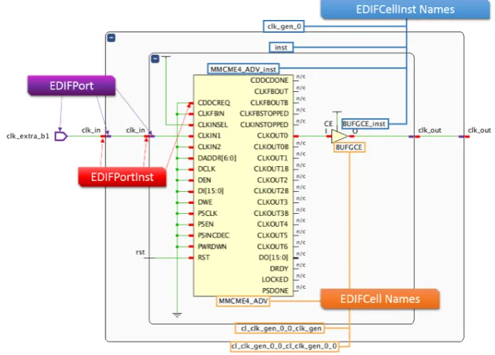
There are two major classes in theDeviceclass, theEDIFNetlist andDesignclass. The ED-IFNetlist class represents the logical netlist which is part of every checkpoint is imported into
RapidWright. TheEDIFCell andEDIFCellInst classes represent a component in the logical
netlist. That can be for example a LUT, flip-flop or an in-output buffer. TheEDIFCell class is
also used to represent a component instance in HDL, however the API is not mature enough to change a hierarchical netlist and it recommends to flatten the design before importing it into RapidWright. Each EDIFCell has one or more EDIFPorts connected. The EDIFPort
and EDIFPortInst classes are used to describe these ports. EDIFPorts are also used to
represent ports on a component instances in a HDL. A overview of these classes can be seen in Figure 2.9. The Design class stores the physical netlist and the constraints. The
physical netlist contains all the information regarding placement and routing. When a placed and routed design is imported into RapidWright using the classes in the Designclass, it is
possible to change the location of certain elements, or just look where the design is placed.
2.4 FPGA delays
One limiting factor to the maximum achievable frequency in a FPGA design is the delay that results from combinational logic and routing. When a signal arrives at an input of a logic circuit it takes some time until the output is starting to change. This is called the
contamination delay. After some time this signal stabilises and that is called thepropagation delay. It also takes time for a signal to travel from one flip-flop to the next one, because
a signal travels at a fixed speed through a conductor. This is called the routing delay. Of
Figure 2.9: An example design showing a overview of how different classes in the ED-IFNetlist class map to ports and cells [9].
[image:16.595.208.378.410.698.2]2.4. FPGADELAYS 11
Figure 2.11: On the left the initial design is shown and on the right a pipeline stage is added [1].
the design.
The maximum frequency a design can have is the maximum delay between two consec-utive flip-flops. Let’s say we have a design that has a delay of 4ns between two flip-flops,
but between two different flip-flops a delay of1ns. In that case the maximum frequency of
the whole design will be the maximum delay, thus fmax = 41ns = 250M Hz. The path that
consists of this maximum delay is also called the critical path. Now to solve this problem additional flip-flops can be added in between these flip-flops and combinational logic. This is called pipelining. As can be seen in figure 2.11, we first start with a design that has a maximum frequency of 250M Hz, but by adding the register in the critical path, the
Chapter 3
Method
There are several methods to increase the maximum achievable frequency of a design. There are 2 main things that can be done, adjusting the design itself or changing the place-ment and routing of the design. This chapter will explain these 2 different methods.
3.1 Automatic Pipelining
As explained in the previous chapter, pipelining is a suitable method to increase the through-put of FPGA designs. However, this becomes quite cumbersome when the designer has to add all these pipeline stages manually, figure out the parallel paths and rerun the synthe-sis/implementation after every iteration. Thus the possibly to do the pipelining automatically was looked into. Ilya Ganusov et al. (2016) [1] describe the process of analysing the netlist to find the flip-flops that can be added as pipeline stages in the design. A summary of how this works will be given in the next section. The authors of this paper are part of Xilinx and added the feature to Vivado. However, the feature only reports which registers can be added to the design and does not automatically adds these registers. In the next chapter it will be explained how this is done automatically.
3.1.1 Netlist Analysis
In an FPGA design not all the paths are like the one in Figure 2.11. The figure shows feed-forward paths only. The output of a flip-flop can also be connected to an input of a LUT that is in the same path. This creates a sequential loop. However, when adding pipeline stages inside such a sequential loop the functional behaviour cannot be guaranteed and thus no pipeline stages can be added to these loops. As can be seen in the Figure 3.1, the behaviour is changed when an extra flip-flop is added in the sequential loop.
The paper describes a method that makes sure that no pipeline stages are added to sequential loops. This starts with modeling the design as a graph. The critical path is known and a flip-flop has to be inserted somewhere in that path. To ensure that flip-flops are also inserted in all the parallel paths of the critical path, every path from I to O must only contain exactly one flip-flop [1]. Figure 3.2 shows an example where this criteria is demonstrated.
Figure 3.1: On the left the initial design with feedback loop and on the right a pipeline stage is added, showing that it chances the behaviour of the design [1].
In the top figure the red line shows two paths that are invalid, because they contain more or less than one flip-flop. However, in the bottom figure the criteria is met. For the complete algorithm the Xilinx paper can be accessed [1].
3.1.2 Iterative Approach
The pipeline report generator that is added to Vivado by [1] is an estimation of the frequency improvement that can be gained. To see if the pipeline stages actually increase the maxi-mum frequency, the registers have to be inserted in the design. The generated report could for example insert 20 pipeline stages at once. The disadvantage of this approach is that the algorithm has no information about the timing during the insertion of the pipeline stages. This is where the iterative approach comes into play. The iterative approach only inserts one pipeline stage, does the placement and timing and then runs the algorithm again such that it can use the newly available timing information. The algorithm is shown in Figure 3.3. According to the Xilinx paper [1] this is the optimal approach and this will be implemented using RapidWright. Now if there are no loops detected, in theory we could add pipeline stages until the maximum frequency of the FPGA is reached.
3.2 Placement
Instead of actually changing the design, it is also possible to change or restrict the placement and/or routing with RapidWright. A method called floorplanning is used for this.
3.2. PLACEMENT 15
Figure 3.2: An invalid pipeline stage on top and a valid pipeline stage below. The red arrows show the invalid paths [1].
ment, on the right logic is restricted to a certain area. [11]
[image:22.595.187.401.84.195.2]Chapter 4
Implementation
Two methods are described in the previous section for improving the throughput of FPGA designs. After some investigation on the feasibility of both methods the pipeline method is chosen and implemented using RapidWright, because at the moment of writing, for such optimizations the placement methods available in RapidWright are not sophisticated enough yet.
The implementation consists of two main parts, which are an implementation in Java using RapidWright and an implementation in Vivado using Tcl commands. The following sections describe these two parts.
4.1 RapidWright
The Java part which actually parses the pipeline report and adds the registers is based on the implementation given in [12]. The implementation used RapidSmith2 which is the predecessor of RapidWright. The code has been ported to RapidWright and some changes have been made. Fortunately the API of RapidWright is similar to that of RapidSmith2. The structure of the code has been changed quite a lot to make the Java program execute faster by using a HashMap instead of the linear algorithm that was used before. Other changes
have been made to make the code more readable.
4.1.1 Automatic pipelining
Using the report pipeline analysis Tcl command, Vivado generates the report which
con-tains all the relevant information to add the pipeline stages [13]. The report can be written to a file and this file is used by the Java program to parse the data. In addition a checkpoint from Vivado is exported which contains the netlist files as discussed in Section 2.3. These two files are passed to the Java program through command-line arguments and imported into relevant Java classes inside the program. RapidWright uses an simple API to import the checkpoint file, namelyDesign.readCheckpoint and the pipeline report is parsed using
the classes: IntraClockSummary,PipelineSummary andCriticalLoops, which corresponds
to the three sections in the pipeline report. Every flip-flop that has to be added, has a
(b) If there are loops, check whether the maximum frequency is reached and quit the program if the maximum frequency is reached.
3. Insert the registers from the pipeline report into a HashMap, where the key is the StartPoint, and the value is a list of EndPoints and then sort the list on the highest
amount of delay.
4. Loop through theHashMapand do the following for every entry:
(a) Take the output port of theStartPoint and loop through theEndPointslist.
(b) Add a flip-flop before everyEndPointand connect the input to theStartPoint.
5. Export the design into a Vivado checkpoint.
4.1.2 Recycling
The pipeline report that Vivado exports can contain pipeline stages that have the same
StartPoint but a different EndPoint. In [12] it was discovered that this can be optimized by
reusing the registers. This is called recycling. As can be seen in Figure 4.1 instead of adding all the registers (Figure 4.1b), less registers can be added and the nets can be reused (Figure 4.1c). Because of this, step 4b listed in the previous section has to be changed. Instead of adding the flip-flops for every EndPoint in the list, we only add the flip-flops for
the first entry in the list ofEndPoints. Because the list is sorted, the first entry will always be
the EndPoint that needs the most delays. All the other EndPoints with less delay but with
the same StartPoint can reuse the flip-flops and connect the EndPoint to correct flip-flop
according to the delay needed.
4.2 Tcl Commands
The iterative approach described in Section 3.1.2 is implemented using Tcl commands in
4.2. TCLCOMMANDS 19
which can be used to for example program the design to hardware, or simulate the design in Vivado.
i f { $argc ! = 3 } {
puts ” Usage: vivado −mode batch −source a u t o . t c l −tclargs <checkpoint> <num of loops>
<max latency added per loop>”
} else {
open checkpoint [lindex $argv 0] place design
for {set i 0} {$ i < [lindex $argv 1]} {incr i} {
r e p o r t p i p e l i n e a n a l y s i s −f i l e p i p e l i n e . t x t −i n c l u d e p a t h s t o p i p e l i n e −max added latency [lindex $argv 2] −report loops
w r i t e c h e c k p o i n t checkpoint.dcp −force w r i t e e d i f c h e c k p o i n t . e d f −force
set s t a t u s [catch {exec −ignorestderr java −jar / home / timon / p i p e l i n e r . j a r checkpoint.dcp p i p e l i n e . t x t >> p i p e l i n e l o g . t x t} r e s u l t ]
i f {$status == 0} {
} e l s e i f {[string equal $::errorCode NONE]} { } else {
switch −exact −− [lindex $::errorCode 0] { CHILDSTATUS {
foreach {− pid code} $::errorCode break i f {$code == 1} {
break
}
}
}
}
open checkpoint c h e c k p o i n t p i p e . d c p place design −unplace
place design
}
4.2. TCLCOMMANDS 21
r e p o r t t i m i n g −f i l e t i m i n g r e s u l t . t x t w r i t e c h e c k p o i n t checkpoint done.dcp −force
f i l e d e l e t e {∗ }[glob ∗. l o g ] f i l e d e l e t e {∗ }[glob ∗. j o u ] f i l e d e l e t e {checkpoint.dcp} f i l e d e l e t e {c h e c k p o i n t . e d f} f i l e d e l e t e {c h e c k p o i n t p i p e . d c p}
}
Chapter 5
Results
For the results, several designs will be tested and the results will be discussed. This will include designs that have sequential loops, but also designs that are already pipelined which can be further pipelined.
5.1 Advanced Encryption Standard (AES)
AES is an encryption standard used by a lot of applications to secure data. Since the research group CAES does a lot of research on AES cores, e.g. how to protect against attacks, it was chosen to test how the pipeline algorithm can increase the throughput of an AES core. There are several implementation of AES, but the unrolled version has no se-quential loops and thus is optimal for pipelining. To compare results with [12], it was chosen to use the exact same VHDL implementation, namely the open-source implementation pro-vided by FreeCores [14]. The design can be synthesised in two ways, using block RAM or using LUTs as RAM. Both options are shown in the results. In addition the design is fully flattened and synthesised inout of context mode. This means that the in and output ports
are not included in the netlist.
Figure 5.1 shows the result of the pipeline implementation for the AES core with LUTs only (DRAM). Before the pipelining the design uses 21% of the LUTs and 7% of the reg-isters on the Zynq FPGA [2]. The design by itself has 30 clock cycles of latency and the x-axis shows the extra latency that is a result of the added pipeline stages. On the left y-axis the increase in maximum frequency is shown. As can be seen in the figure the maximum frequency increases significantly up till 28%, depending on the amount of latency that is desirable. The frequency increases exponentially and thus the most performance can be gained when adding the first pipeline stages. The number of registers added increases lin-early and is in the order of 10000 registers.
The other version of the AES core uses BRAM to implement the memory. With this implementation less LUTs are being used. The results are shown in Figure 5.2. With this implementation the exponential increase in frequency is less steep than Figure 5.1. How-ever, it ends up with almost the same frequency increase of 25%. The linear increase in
Figure 5.1: Showing the maximum frequency and the number of registers added when run-ning the pipeline algorithm for the AES core with LUTs only.
registers is similar to Figure 5.1. Post implementation simulations show that the behavior of the design is not changed and it outputs the correct result for a known input. However, be-cause of the added latency the simulation needs to wait more clock cycles to get the correct output.
5.1.1 AES core with feedback loop
The CAES group of the University of Twente provided another implementation of AES which is different than the previous implementation and does have sequential loops. This limits the pipelining which results in only one pipeline stage that can be added. The design starts with a maximum frequency of 206.61M Hz and after the added pipeline stage has a maximum
frequency of223.51M Hz. This is an increase of 8%.
5.2 8 Bit Multiplier
The algorithm is also tested on a 8 bit multiplier. This multiplier is a pipelined multiplier and it should be able to take advantage of that. The code is hosted on Github [15]. The results are shown in Figure 5.3. As can be seen in the figure, the design starts with a maximum frequency of 250M Hz and stabilizes around a frequency of 410M Hz. This is a increase
5.2. 8 BITMULTIPLIER 25
Figure 5.2: Showing the maximum frequency and the number of registers added when run-ning the pipeline algorithm for the AES core including BRAMs.
[image:31.595.76.516.456.703.2]pipelined version of AES to the version with sequential loops, significant gain was achieved in maximum frequency. For the unrolled AES implementation, the difference in maximum frequency between the BRAMs and LUTs (DRAM) design is not significant. This is because the AES core is a big design, which results in a lot of resources being spread out over the FPGA and thus the routing delay caps the maximum frequency. Comparing results with [12], these results show an improvement of 7%. This shows that the iterative approach can make use of the extra timing information available.
5.3.2 8 Bit Multiplier
Another trade off for the 8 bit multiplier is whether it can be replaced by a DSP slice. There can be designs where there is no space anymore to use a DSP slice, or where there are enough LUTs to use. The maximum frequency a DSP slice can have is 257.47M HZ [16].
Now the 8 bit multiplier can reach a maximum frequency up till410M Hz. This could be used
instead of a hardware multiplier when only 8 bits are used and if the latency is acceptable.
5.3.3 Latency versus Throughput
Chapter 6
Conclusion and recommendations
6.1 Conclusion
From the results it can be concluded that adding pipeline stages to some designs signifi-cantly improve throughput, with some overhead of the added latency and the extra registers. But since the FPGAs of nowadays have more resources available, the overhead of the added registers is less significant. One downside is that designs with sequential loops cannot take advantage of the pipeline method, since the functional behaviour cannot be guaranteed.
The increase in throughput depends on the size of the design, but also on the type of resources being used. This has been shown with the AES core. The maximum frequency increase is achievable for small designs where the flip-flops and LUTs can be placed close together, which in turn also increases the throughput. For big designs the improvement is less.
Furthermore, the results show that RapidWright is a perfect tool to change the design with Java code. In these results only the netlist editing functionality of RapidWright has been used, but examples in RapidWright show that for placing and routing RapidWright can be used too. This has not been tested in this thesis.
6.2 Recommendations
In addition to the work done in this thesis, the placement method described was not imple-mented. A recommendation would be to try to add the placement method to RapidWright and see if this would also increase the throughput of FPGA designs. RapidWright is able to do the placement and routing, but this has not been tested. Moreover, more designs should be evaluated to harden the results.
Post implementation simulations show that the output does not change, but that is not a assurance that the design also behaves the same on physical hardware. Measurement should be done to confirm that the design did not change with the extra added pipeline stages.
Bibliography
[1] A. N. R. T. P. Ilya Ganusov, Henri Fraisse and S. Das, “Automated extra pipeline anal-ysis of applications mapped to xilinx ultrascale+ fpgas,”Field Programmable Logic and Applications (FPL), 2016 26th International Conference, pp. 1–10, 2016.
[2] “Product brief zedboard,” 2018. [Online]. Available: ”http://zedboard.org/sites/default/ files/product briefs/5066-PB-AES-Z7EV-7Z020-G-V3c%20%281%29 0.pdf”
[3] “7 series fpgas configurable logic block ug474,” September 2016. [Online]. Available: ”https://www.xilinx.com/support/documentation/user guides/ug474 7Series CLB.pdf”
[4] “7 series fpgas memory resources ug473,” February 2019. [Online]. Available: ”https://www.xilinx.com/support/documentation/user guides/ug473 7Series Memory Resources.pdf”
[5] “7 series dsp48e1 slice ug479,” March 2018. [Online]. Available: ”https: //www.xilinx.com/support/documentation/user guides/ug479 7Series DSP48E1.pdf”
[6] “Vivado design suite user guide ug892,” June 2018. [Online]. Available: ”https://www.xilinx.com/support/documentation/sw manuals/xilinx2018 2/ ug892-vivado-design-flows-overview.pdf”
[7] “Xilinx design flow,” 2018. [Online]. Available: ”https://www.aldec.com/en/solutions/ fpga design/fpga vendors support/xilinx--xilinx-fpga-design-flow”
[8] “Vivado design suite user guide using constraints,” 2018. [Online]. Available: ”https://www.xilinx.com/support/documentation/sw manuals/xilinx2018 1/ ug903-vivado-using-constraints.pdf”
[9] “Rapidwright.” [Online]. Available: ”http://www.rapidwright.io”
[10] J. Rajewski, “Fpga timing,” January 2018. [Online]. Available: ”https://alchitry.com/ blogs/tutorials/fpga-timing”
[11] B. Gunther, “Floorplanning large fpgas,” 2011. [Online]. Available: ”http://www.users. on.net/∼bkgunther/design/floorplanning.html”
[12] R. van Loo, “Increasing throughput of fpga-based streaming applications by using pipelining,” Bachelor thesis, University of Twente, 2018.
![Figure 2.1: Overview of a CLB in a Xilinx FPGA, showing the connections to other CLBsand the switch matrix [3].](https://thumb-us.123doks.com/thumbv2/123dok_us/9629233.465429/10.595.212.381.85.239/figure-overview-xilinx-showing-connections-clbsand-switch-matrix.webp)
![Figure 2.3: Configurations for LUT inside a SLICEM slice [3].](https://thumb-us.123doks.com/thumbv2/123dok_us/9629233.465429/11.595.344.508.366.646/figure-congurations-for-lut-inside-a-slicem-slice.webp)
![Figure 2.5: Overview of the DSP48E1 slice [5].](https://thumb-us.123doks.com/thumbv2/123dok_us/9629233.465429/12.595.165.424.90.214/figure-overview-of-the-dsp-e-slice.webp)
![Figure 2.6: Overview of the Vivado design flow for Xilinx FPGAs [7].](https://thumb-us.123doks.com/thumbv2/123dok_us/9629233.465429/13.595.209.379.85.297/figure-overview-vivado-design-ow-xilinx-fpgas.webp)
![Figure 2.7: Interface between RapidWright and Vivado using checkpoints [9].](https://thumb-us.123doks.com/thumbv2/123dok_us/9629233.465429/14.595.186.407.82.304/figure-interface-rapidwright-vivado-using-checkpoints.webp)
![Figure 2.8: Hierarchical structure of Xilinx FPGAs [9]](https://thumb-us.123doks.com/thumbv2/123dok_us/9629233.465429/15.595.142.452.83.310/figure-hierarchical-structure-of-xilinx-fpgas.webp)
![Figure 2.11: On the left the initial design is shown and on the right a pipeline stage is added[1].](https://thumb-us.123doks.com/thumbv2/123dok_us/9629233.465429/17.595.109.485.97.260/figure-initial-design-shown-right-pipeline-stage-added.webp)
![Figure 3.1: On the left the initial design with feedback loop and on the right a pipeline stageis added, showing that it chances the behaviour of the design [1].](https://thumb-us.123doks.com/thumbv2/123dok_us/9629233.465429/20.595.112.482.86.236/figure-initial-feedback-pipeline-stageis-showing-chances-behaviour.webp)
![Figure 3.2: An invalid pipeline stage on top and a valid pipeline stage below. The red arrowsshow the invalid paths [1].](https://thumb-us.123doks.com/thumbv2/123dok_us/9629233.465429/21.595.145.444.132.374/figure-invalid-pipeline-stage-valid-pipeline-arrowsshow-invalid.webp)
![trans Di μ chlorido bis{chlorido[tris(3,5 dimethylphenyl)phosphane κP]palladium(II)} dichloromethane monosolvate](data:image/gif;base64,R0lGODlhAQABAIAAAP///wAAACH5BAEAAAAALAAAAAABAAEAAAICRAEAOw==)