warwick.ac.uk/lib-publications
Original citation:Ortiz Gonzalez, Jose Angel, Alatise, Olayiwola M., Ran, Li, Mawby, P. A. (Philip A.), Rajaguru, Pushparajah and Bailey, Christopher (2017) An initial consideration of silicon carbide devices in pressure-packages. In: 2016 IEEE Energy Conversion Congress and Exposition (ECCE), Milwaukee, WI, 18-22 Sep 2016. Published in: 2016 IEEE Energy Conversion Congress and Exposition (ECCE).
Permanent WRAP URL:
http://wrap.warwick.ac.uk/86129
Copyright and reuse:
The Warwick Research Archive Portal (WRAP) makes this work by researchers of the University of Warwick available open access under the following conditions. Copyright © and all moral rights to the version of the paper presented here belong to the individual author(s) and/or other copyright owners. To the extent reasonable and practicable the material made available in WRAP has been checked for eligibility before being made available.
Copies of full items can be used for personal research or study, educational, or not-for profit purposes without prior permission or charge. Provided that the authors, title and full bibliographic details are credited, a hyperlink and/or URL is given for the original metadata page and the content is not changed in any way.
Publisher’s statement:
“© 2017 IEEE. Personal use of this material is permitted. Permission from IEEE must be obtained for all other uses, in any current or future media, including reprinting
/republishing this material for advertising or promotional purposes, creating new collective works, for resale or redistribution to servers or lists, or reuse of any copyrighted component of this work in other works.”
A note on versions:
The version presented here may differ from the published version or, version of record, if you wish to cite this item you are advised to consult the publisher’s version. Please see the ‘permanent WRAP URL’ above for details on accessing the published version and note that access may require a subscription.
An Initial Consideration of Silicon Carbide Devices
in Pressure-Packages
Jose Angel Ortiz Gonzalez Student Member, IEEE,
Olayiwola Alatise, Li Ran Senior Member, IEEE,
and Phil Mawby Senior Member, IEEE
School of Engineering University of Warwick Coventry, United Kingdom [email protected]
Pushparajah Rajaguru and Christopher Bailey Senior
Member, IEEE,
Computational Mechanics and Reliability Group University of Greenwich
London, United Kingdom
Abstract—Fast switching SiC Schottky diodes are known to exhibit significant output oscillations and electromagnetic emissions in the presence of parasitic inductance from the package/module connections. Furthermore, solder pad delamination and wirebond lift-off are common failure modes in high temperature applications. To this end, pressure packages, which obviate the need for wire-bonds and solder/die attach, have been developed for high power applications where reliability is critical like thyristor valves in HVDC line commutated converters. In this paper, SiC Schottky diodes in pressure-packages (press-pack) have been designed, developed and tested. The electrothermal properties of the SiC diode in press-pack have been tested as a function of the clamping force using different thermal contacts, namely molybdenum and Aluminum Graphite. Finite Element Simulations have been used to support the analysis.
Keywords— Press-Pack; silicon carbide; Schottky diode; aluminum graphite; molybdenum
I. INTRODUCTION
A Press-pack module [1] is a packaging system where the semiconductor is pressed between two copper poles using an intermediate contact material of similar Coefficient of Thermal Expansion (CTE), typically molybdenum. The thermal and electrical contact is generated by means of applying an external force and the reliability concerns of the traditional packaging systems are removed due to the elimination of the traditional failure elements like the solder/die attach and wire bonds [2].
Press-pack modules have been extensively used for large area semiconductor devices like high power silicon diodes and thyristors traditionally for grid connected line-commutated converters in FACTS and HVDC applications. More recently, small area silicon devices like diodes and IGBTs using a multichip module approach [1] have been developed in an effort to use press-pack technology in self-commutated voltage source converters. Some of the benefits of this packaging system, in addition to the extended reliability, are double side cooling, a compact design and the limited number of interconnections within the module. On the other hand, the lack of dielectric insulation in the module and a more complex assembly system are the major trade-offs [1]. Press-pack
modules are currently commercially available for silicon devices but only few studies have been done for silicon carbide devices [3], [4]. The limitations of the traditional packaging systems for SiC technology [5] and the availability of larger area silicon carbide dies, which may reduce the mechanical complexity of the press-pack module design, suggest that the study of the properties, performance and benefits of silicon carbide press-pack power modules is timely and appropriate. This is more so the case given the aforementioned concerns about the power cycling capability of SiC in traditional packages and the better power cycling capability demonstrated in [4].
In section II, a prototype for the evaluation of silicon carbide devices using pressure contacts is presented and the study of Aluminum Graphite (ALG) [6] as an alternative to the traditional intermediate contact made of molybdenum is proposed. In section III, the use of Finite Element Analysis (FEA) for evaluating the proposed alternatives, including thermal analysis and stress analysis, is presented. Section IV presents experimental measurements, where the thermal performance of the device has been analyzed for different intermediate contact materials and different clamping forces, including the initial evaluation of double side cooling, and section V concludes the paper.
II. PROTOTYPE OF A SILICON CARBIDE SCHOTTKY DIODE IN
PRESS-PACK
The integration of silicon carbide in press-pack assemblies follows the multichip approach already used with silicon IGBT press-pack modules, with the added complexity of the smaller size of the silicon carbide chips compared with the contemporary silicon chip. This reduced chip size is a result of the manufacturing requirements to keep the defects at wafer level low [7] and is enabled by the improved specific on-state resistance of silicon carbide devices. The small die sizes result in lower parasitic capacitances, hence, reduced switching losses coupled with the reduced conduction losses from smaller on-state resistance. The device selected for the first evaluation of pressure contacts on silicon carbide is a 1.2 kV/50 A Schottky diode from Cree/Wolfspeed with datasheet reference CPW5-1200-Z050B [8]. The die size is 4.9 mm by 4.9 mm,
with an anode opening of 3.8 mm by 3.8 mm and a thickness of 380 μm.
Although the press-pack assembly can be used for multichip modules with high current capability, the initial evaluation of the press-pack SiC Schottky diode is done using a single die prototype shown in Fig. 1. Fig. 1(a) and 1(b) show the mechanical drawings of the press-pack assembly while Fig. 1(c) shows the assembled prototype. A prototype of a 1.2 kV/200 A SiC Schottky diode module using 4 CPW5-1200-Z050B dies is shown in Fig. 2. A 3D model of the prototype without the external case is shown in Fig. 2 (a), while the initial assembly is shown in Fig. 2(b).
Fig. 1: (a) Model of the press-pack Schottky diode, (b) Cross-section of the model with the external case, (c) Assembled prototype
Fig. 2: (a) Model of the press-pack Schottky diode module, (b) Top view of the module with the external case and die carriers
The anode and cathode poles are made of copper, with a nickel plating of 5 µm. A die carrier, which is made of polyphenylene sulfide (PPS), is used for aligning the die and the intermediate contacts within the assembly while a polyether ether ketone (PEEK) element is used as external case for positioning the copper poles of the assembly. Both PPS and PPEK are engineering plastics [9], with similar properties, including an operating temperature of over 220 °C, dimensional stability, good machinability and UL94/VO compliance. This prototype is for the evaluation of the pressure contact and is therefore not hermetically sealed as it would be in a traditional press-pack module, hence the maximum operating voltage for the switching tests is limited.
The usual intermediate contact material for matching the CTE of the semiconductor and the copper poles is molybdenum. ALG is a Metal Matrix Composite (MMC) produced by pressure infiltration of porous graphite by liquid aluminum. According to Schunk Hoffmann Carbon Technology [6], this new composite incorporates the advantageous properties of both materials and can be used as an alternative to molybdenum in press-pack modules because of its suitable CTE and thermal conductivity. The type of ALG that was used in this study is ALG 2208. The cathode contact made of Aluminum Graphite can be seen in Fig. 3. In Fig. 3(b) the structure composed of aluminum and graphite can be clearly observed.
Fig. 3: (a) Cathode contact made of ALG, (b) Detail of the ALG structure
ALG 2208 is an anisotropic material with the following material properties [6]:
• Density: 2.3 g/cm3
• Specific electric resistance: x/y=0.4, z= 0.6 µΩ·m
• Coefficient of thermal expansion: x/y=8,z=12 μm/m·K
• Thermal conductivity: x/y=220, z=140 W/m·K
• Specific heat capacity: 800 J/kg·K at 25 °C
[image:3.612.60.291.201.400.2]The cathode contact made of molybdenum is shown in Fig. 4. Molybdenum is the usual intermediate contact material for press-pack modules, for multichip IGBT modules and large area thyristor discs. The properties of molybdenum [10] are:
• Density: 10.22 g/cm3
• Specific electric resistance: 0.053 µΩ·m
• Coefficient of thermal expansion: 5.35 μm/m·K
• Thermal conductivity: 138 W/m·K
• Specific heat capacity: 217 J/kg·K at 25 °C
Fig. 4: (a) Cathode contact made of molybdenum, (b) Detail of the molybdenum contact
[image:3.612.316.567.213.316.2] [image:3.612.48.295.437.542.2] [image:3.612.317.562.556.659.2]intermediate contact. The surface roughness and flatness also have an influence on the thermal and electrical contact [11], [12], hence all these variables have been considered on the FEA simulations done in this paper.
The dimensions of the intermediate contacts are 3.7 mm by 3.7 mm for the anode contact and 4.9 mm by 4.9 mm for the cathode contact, with a thickness of 1.5 mm for both contacts. The contacts have been machined with a 0.5 mm radius and the pressed area is 23.80 mm2 for the cathode contact and 13.48
mm2 for the anode contact. The assembled diode, without the
[image:4.612.111.244.199.305.2]external case, is shown in Fig. 5.
Fig. 5: Assembled press-pack diode without the external case
According to [1], the pressure for optimal thermal and electrical contact is 10 to 20 N/mm2. Box clamps BX-42 from
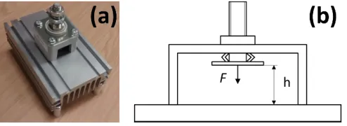
GD Rectifiers [13] rated at 300 N and 500 N for the nominal length of the press-pack prototype (19.38 mm) have been prepared, allowing the evaluation of the module using single side cooling. The heatsink used for the initial measurements is a PS136-150B from GD Rectifiers [13] and the assembly of the heatsink and the clamp is shown in Fig. 6(a). The clamp uses a spring for applying the rated force at the nominal height and the operation of the box clamp is shown in Fig. 6(b).
Fig. 6: (a) Clamp BX-42 and heatsink PS136-150B assembly, (b) Operating mechanism of the BX-42 box clamp
III. FINITE ELEMENT ANALYSIS OF THE PERFORMANCE OF A
SILICON CARBIDE SCHOTTKY DIODE ON PRESS-PACK
A multi-physics finite element simulation analysis of the press-pack diode presented has been done. One quarter model has been generated in ANSYS mechanical software and the complexity of the model structure for the FEA simulation was further reduced by substituting the heatsink in the model with an equivalent heat transfer coefficient. The heat transfer coefficient the heatsink model PS136/150B was approximated as 4991 W/m2K. Other material properties were extracted from
manufacturer specifications and public sources. In the finite element model, rather than applying the direct pressure, a
spring load was applied which can mimic the BX-42 clamp pressure mechanism shown in Fig. 6(b) and the spring constant value was evaluated from the mechanical simulation.
[image:4.612.316.562.276.389.2]Analytical models widely cited in the literature [10]-[12] were used to estimate the thermal and electrical contact resistances. A direct multi-physics coupling analysis involving electro-thermo-mechanical interactions which approximate the joule heating and the resulting thermally induced deformation and stresses on structure on the press-pack module was numerically simulated in the finite element software. The numerical models for a set of load current, clamping pressure and two different contact pad materials (molybdenum or ALG) have been simulated. Fig. 7 shows the temperature distribution for the press-pack assembly when molybdenum contacts are used, for a clamping force of 300 N and load currents of 10 A and 20 A. Fig. 8 presents the simulation results for ALG contacts. In both figures it can be observed that the temperature increases as the load current increases.
Fig. 7: Temperature distribution for the press-pack assembly using molybdenum contacts. Clamping force 300 N, load current: (a) 10 A, (b) 20 A
Fig. 8: Temperature distribution for the press-pack assembly using ALG contacts. Clamping force 300 N, load current: (a) 10 A, (b) 20 A
The clamping force also affects the temperature on the assembly as it is shown in Fig. 9, where the temperature distribution on the diode is shown when molybdenum contacts are used, and in Fig. 10, when ALG contacts are used. Comparing the results shown on Fig. 9 and Fig. 10, the temperature on the diode is lower when ALG contacts are used. For both contact materials the temperature decreases when the clamping force increases.
[image:4.612.317.561.421.531.2] [image:4.612.46.293.455.545.2]Fig. 9: Temperature distribution on the SiC diode using molybdenum contacts. Load current 20 A, (a) clamping force 300 N, (b) 500 N
Fig. 10: Temperature distribution on the SiC diode using ALG contacts. Load current 20 A, (a) clamping force 300 N, (b) 500 N
Fig. 11: Temperature distribution on the SiC diode for a clamping force of 500 N and a load current 20 A. Contact material: (a) molybdenum, (b) ALG
[image:5.612.51.292.208.321.2]In Fig. 11, it can be clearly observed that the temperature distribution on the SiC chip is higher when molybdenum contacts are used. The models where molybdenum contacts are used generated higher average temperature in the silicon carbide chip in comparison with the models where the ALG contact and using data obtained from different simulations, the average temperature on the diode was calculated for both contact materials and different clamping forces. The results are presented in Fig. 12, where the effect of the clamping force is evaluated for ALG and molybdenum contacts at a load current of 20 A. Fig. 13 shows the impact of the load current and contact material for a clamping force of 500 N. One of the main conclusions from the data presented on Fig. 13 is that when using ALG contact, the load current for the same junction temperature is higher.
[image:5.612.344.532.227.371.2]Fig. 12: Average chip temperature as function of the clamping force for ALG and Mo contacts. Load current 20 A
Fig. 13: Average chip temperature as function of the load current for ALG and Mo contacts. Clamping force 500 N
The clamping force has an impact on the thermal performance of the assembly, however increasing the pressure generates higher stresses on the diode. The von Mises stress distribution on the chip for contact pads of molybdenum and ALG are presented in Fig. 14 and Fig. 15 respectively, for a load current of 20 A and clamping forces of 300 N and 500 N. According to the FEA results the chip with the ALG contact pads exhibits higher stress distribution in comparison with chip with molybdenum contact pads. The maximum von Mises stress on the chip from the FEA simulations is 164 MPa when molybdenum contacts are used and 158 MPa when ALG contacts are used. These values are lower than the fracture strength of SiC given in [14], in the range of 0.5 to 1.5 GPa.
[image:5.612.55.283.358.476.2] [image:5.612.323.551.555.669.2]Fig. 15: Von Mises stress distribution on the SiC diode using ALG contacts. Load current 20 A, clamping force: (a) 300 N, (b) 500 N
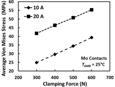
The average von Mises stress on the diode chip from the numerical simulations, as a function of the clamping force for the different contact materials and a load current of 20 A, is presented in Fig. 16. As the stress distributions in Fig. 14 and Fig. 15 indicate, the average stresses are higher when ALG contacts are used.
[image:6.612.331.549.153.233.2]Fig. 17 shows the average von Mises stress on the diode when molybdenum contacts are used, as function of the clamping force for two different load currents, namely 10 A and 20 A. The induced thermomechanical stresses are higher due to the higher self-heating caused by increasing the load current.
Fig. 16: Average von Mises stress on the SiC diode as function of the clamping force for ALG and molybdenum contacts. Load current: 20 A
Fig. 17: Average von Mises stress on the SiC diode as function of the clamping force, using molybdenum contacts. Load current 10 A and 20 A
IV. EXPERIMENTAL RESULTS
The experimental verification of the FEA results has been done using the test setup shown in Fig. 18. Constant current DC heating tests [15], using the press-pack assembly shown in Fig. 6(a) as Device Under Test (DUT), have been performed for evaluating the impact of the contact material and the clamping force on the junction temperature increase.
Fig. 18: Electrical schematic of the DC heating test setup
[image:6.612.80.263.363.503.2]The voltage drop across the diode at low currents has been used as Temperature Sensitive Electrical Parameter (TSEP) for the estimation of the junction temperature [16]. At low current densities, the forward voltage decreases with increasing temperature in a linear relation. The calibration of the TSEP has been done using a thermal chamber to set the junction temperature. The forward voltage has been measured using a small sensing current ISENSE at different temperatures when the voltage across the diode reached steady state. This allows the assumption that the junction temperature equals the temperature of the thermal chamber. This time was around 60 minutes.
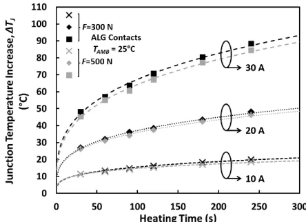
Fig. 19 shows the relationship between the junction temperature and the forward voltage for the silicon carbide Schottky diode in a press-pack module with ALG contacts at different clamping forces, while Fig. 20 presents calibration when molybdenum contacts are used. The temperature coefficient, or K- factor, is the slope of the trend line and it is around -1.5 mV/°C for the different contacts and clamping forces. Increasing the clamping force reduces the contact resistance, thus slightly reducing the forward voltage at low currents when ALG contacts are used as shown in Fig. 19. In the case of the molybdenum contacts, the impact of the clamping force on the TSEP could be considered negligible.
[image:6.612.77.263.538.679.2]Fig. 19: Calibration curves for the SiC Schottky diode using ALG at different clamping forces
Fig. 20: Calibration curves for the SiC Schottky diode using molybdenum at different clamping forces
Fig. 21: Comparison between the calibration curve using ALG and molybdenum contacts for a clamping force of 500 N
The heating tests were performed at different clamping forces, for different contact materials and different load currents. Fig. 22 and Fig. 23 show the impact of the clamping force for ALG and molybdenum contacts on the transient heating respectively. Increasing the clamping force improves the thermal contact resistances for both materials, hence the junction temperature increase is lower. Fig. 24 analyzes the impact of the contact material and it is clearly observed that the use of ALG contacts improves the thermal performance of the press-pack diode. Comparing the results shown in Fig. 22, Fig. 23 and Fig. 24 it can be seen that from the point of view of the thermal performance, the intermediate contact material has a higher impact on the reduction of the temperature increase than the clamping force. These results follow the trend shown in the
simulations and suggest a better thermal performance of the ALG contacts.
[image:7.612.81.264.224.360.2]Increasing the power density requires better cooling methods and one of the benefits of the press-pack technology is the possibility of double side cooling. The double side cooling has been evaluated using a heatsink model PS185/150B and a clamp model BC79D rated at 400 N, both from GD Rectifiers [13]. The assembled system is shown in Fig. 25.
[image:7.612.331.557.346.508.2]Fig. 22: Impact of clamping force on the junction temperature increase for ALG contacts during DC heating tests
Fig. 23: Impact of clamping force on the junction temperature increase for molybdenum contacts during DC heating tests
[image:7.612.81.265.390.525.2] [image:7.612.333.553.536.694.2]Fig. 25: Double side cooling assembly of the press-pack diode
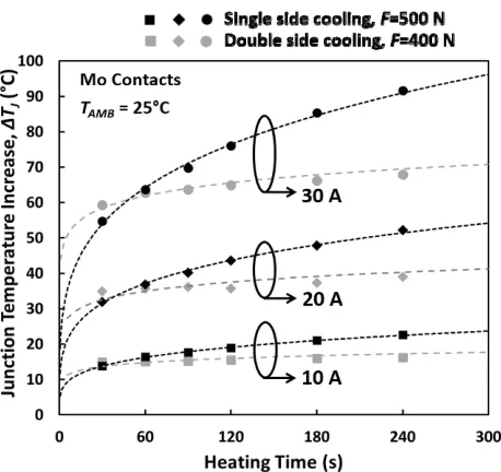
The double side cooling tests were performed using molybdenum as intermediate contact and the results are presented in Fig. 26, where the junction temperature increase is compared for double side cooling and single side cooling. The impact of the double side cooling is considerable in reducing the junction temperature increase by an average of 26 % at a lower clamping force thereby reducing the mechanical stresses on the chip.
Fig. 26: Impact of double side cooling on the junction the junction temperature increase
V. CONCLUSIONS
This paper has investigated the design, development and testing of silicon carbide Schottky diodes in a press-pack assembly. The impact of the clamping force on the thermal transients has been explored for Aluminum Graphite and molybdenum intermediate contacts. Preliminary results show that the choice of contact material is critical and the diodes with Aluminum Graphite contacts exhibit lower junction temperatures. Finite element simulations show that the stresses on the diodes with ALG contacts are higher than those with molybdenum. Double side cooling, at a reduced clamping force, improves the cooling of the diode and a lower operating junction temperature is achieved with reduced mechanical stresses on the diode. The studies performed on this paper focus on the impact of the intermediate contact material for a single die module. A multiple die module has been proposed
and further research has to be done, for analyzing the impact of the uneven pressure distribution between the dies and the reliability of the diode. The elimination of the wirebonds and solder suggests a higher reliability for this packaging system and more research on failure mechanisms for press-pack modules and assemblies has to be done as the existing information is limited.
ACKNOWLEDGMENT
The authors wish to thank Schunk Hoffmann Carbon Technology AG, GD Rectifiers Ltd. and Röchling Fibracon Ltd. for their support on this paper.
REFERENCES
[1] J. Lutz, H. Schlangenotto, U. Scheuermann and R. D. Doncker,
Semiconductor power devices: Physics, characteristics, and reliability.
Springer Verlag, 2011.
[2] M. Ciappa, “Selected failure mechanisms of modern power modules,” Microelectronics Rel., vol. 42, no. 4–5, pp. 653–667, April–May 2002 [3] Y. Sugawara et al., "3 kV 600 A 4H-SiC high temperature diode
module," Power Semiconductor Devices and ICs, 2002. Proceedings of the 14th International Symposium on, 2002, pp. 245-248
[4] V. Banu, P. Godignon, et Al. “Enhanced power cycling capability of SiC Schottky diodes using press pack contacts”, Microelectronics Rel.,Volume 52, no. 9-10, pp. 2250-2255, September–October 2012 [5] C. Herold, M. Schaefer, F. Sauerland, T. Poller, J. Lutz and O. Schilling,
"Power cycling capability of modules with SiC-diodes," Integrated Power Systems (CIPS), 2014 8th International Conference on, Nuremberg, Germany, 2014, pp. 1-6.
[6] Schunk Hoffmann Carbon Technology AG, Aluminium Graphite
composites brochure [Online]. Available: www.hoffmann.at
[7] M. Loboda (2013) Considerations for designing power electronic
devices based on advanced SiC technologies [Online], Available:
http://www.dowcorning.com/
[8] Cree/Wolfspeed. CPW5-1200-Z050B Datasheet [Online]. Available: http://www.wolfspeed.com/
[9] Röchling. PPS and PEEK properties [Online]. Avalilable: http://www.roechling.com/en/home.html
[10] P. Rajaguru, H. Lu, C. Bailey, J. Ortiz-Gonzalez and O. Alatise, "Electro-thermo-mechanical modelling and analysis of the press pack diode in power electronics," Thermal Investigations of ICs and Systems (THERMINIC), 2015 21st International Workshop on, Paris, 2015, pp. 1-6
[11] M. M. Yovanovich, "Four decades of research on thermal contact, gap, and joint resistance in microelectronics," in IEEE Transactions on Components and Packaging Technologies, vol. 28, no. 2, pp. 182-206, June 2005.
[12] P. G. Slade, Electrical contacts, principles and applications, 2nd edition,
CRC Press, 2014
[13] GD Rectifiers Ltd [Online], Available: http://www.gdrectifiers.co.uk/ [14] W. N. Sharpe, G. M. Beheim, L. J. Evans, N. N. Nemeth and O. M.
Jadaan, "Fracture strength of single-crystal silicon carbide microspecimens at 24 °C and 1000 °C," in Journal of Microelectromechanical Systems, vol. 17, no. 1, pp. 244-254, Feb. 2008. [15] L. R. GopiReddy, L. M. Tolbert and B. Ozpineci, "Power cycle testing of power switches: A literature survey," in IEEE Transactions on Power Electronics, vol. 30, no. 5, pp. 2465-2473, May 2015.
[image:8.612.58.287.280.496.2]