Application Note AN-1138
IRS2092(S) Functional Description
By Jun Honda, Xiao-chang Cheng, Wenduo Liu
Table of Contents
Page
General Description... 1
Typical Implementation... 1
PWM Modulator... 3
MOSFET Selection... 6
Protection Design ... 7
Deadtime Generator... 12
Power Supply ... 14
Junction Temperature Estimation... 15
IRS2092(S) General Description
The IRS2092(S) is a Class D audio amplifier driver with integrated PWM modulator and over current protection. Combined with two external MOSFETs and a few external components, the IRS2092(S) forms a complete Class D amplifier with dual over current, and shoot-through protection, as well as UVLO protection for the three bias supplies. The versatile structure of the analog input section with an error amplifier and a PWM comparator has the flexibility of implementing different types of PWM modulator schemes.
Loss-less current sensing utilizes RDS(on) of the
MOSFETs. The protection control logic monitors the status of the power supplies and load current across each MOSFET.
For the convenience of half bridge configuration, the analog PWM modulator and protection logic are constructed on a floating well.
The IRS2092(S) implements start-up click noise elimination to suppress unwanted audible noise during PWM start-up and shut-down.
Typical Implementation
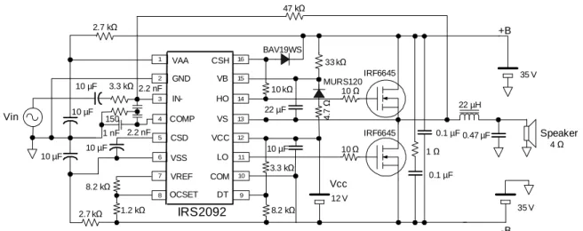
The following explanations are based on a typical application circuit with self-oscillating PWM topology shown in Figure 1. For further information, refer to the IRAUDAMP5 reference design.
Input Section
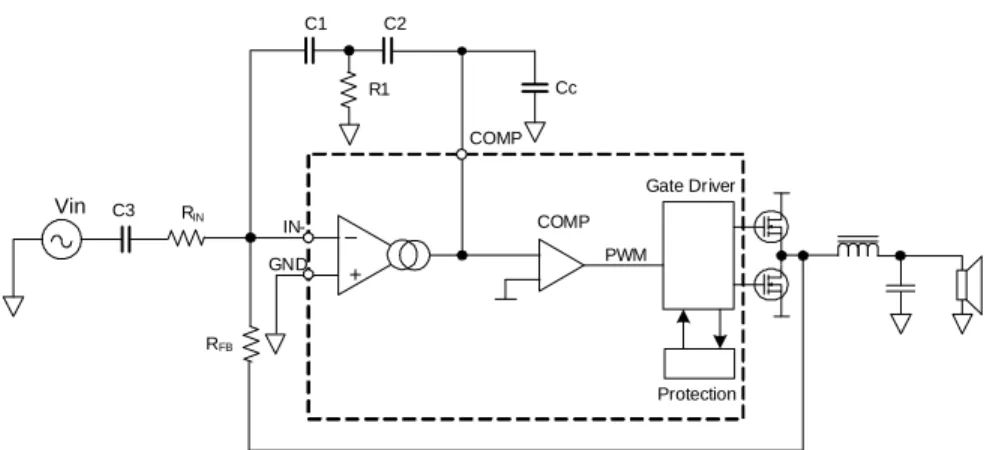
The audio input stage of IRS2092(S) is configured as an inverting error amplifier.
In Figure 2, the voltage gain of the amplifier GV is
determined by input resistor RIN and feedback
resistor RFB.
IN FB V
R
R
G
=
Since the feedback resistor RFB is part of an
integrator time constant, which determines switching frequency, changing overall voltage gain by RIN is
simpler and, therefore, recommended in most cases.
Note that the input impedance of the amplifier is equal to the input resistor RIN.
A DC blocking capacitor C3 should be connected in series with RIN to minimize DC offset in the output. A
ceramic capacitor is not recommended due to potential distortion. Minimizing DC offset is essential for audible noise-less Turn-ON and -OFF.
The connection of the non-inverting input IN+ is a reference for the error amplifier, and thus is crucial for audio performance. Connect IN+ to the signal reference ground in the system, which has same potential as the negative terminal of the speaker output.
IRS2092
12 V
Vin
-B Vcc
+B
4 Ω
35 V 35 V
0.47 µF 22 µH 33 kΩ
10 Ω
4
.7
Ω
22 µF
MURS120
10 µF 10 Ω
IRF6645 IRF6645 47 kΩ
150 3.3 kΩ
10 µF
10 µF 1 nF 2.2 nF 10 µF
0.1 µF 10 µF
3.3 kΩ
8.2 kΩ
2.2 nF 2.7 kΩ
2.7 kΩ
8.2 kΩ
1.2 kΩ
10 kΩ
BAV19WS
0.1 µF 1 Ω
VAA GND
IN-OCSET COM COMP
VSS LO
VCC
VREF HO VS CSD
CSH VB
DT
2
16 1
4 3
5 6 7 8
15 14 13 12 11 10 9
Speaker
COMP PWM
Gate Driver
Protection
Vin
C1 C2
R1
RFB RIN
+
COMP
GND IN-C3
Cc
Figure 2 IRS2092(S) Typical Control Loop Design OTA
The front end error amplifier of the IRS2092(S) features an operational trans-conductance amplifier (OTA), which is carefully designed to obtain optimal audio performance. The OTA outputs a current output to the COMP pin, unlike a voltage output in an operational amplifier (OPA). The non-inverting input is internally tied to the GND pin.
The inverting input has clamping diodes to GND to improve recovery from clipping as well as ensuring stable start up. The OTA output COMP is internally connected to the PWM comparator whose threshold is (VAA-VSS)/2.
For stable operation of the OTA, a compensation capacitor Cc minimum of 1nF is required.
The OTA is shut off when VCSD<Vth2.
PWM Modulator
The IRS2092(S) allows the user to choose from numerous ways of PWM modulator
implementations. In this section, all the
explanations are based on a typical application circuit of a self oscillating PWM.
Self-Oscillating PWM Modulator Design
The typical application features self oscillating PWM scheme. For better audio performance, 2nd order integration in the front end is chosen.
Self-Oscillating Frequency
Self oscillating frequency is determined mainly by the following items in Figure 2.
· Integration capacitors, C1 and C2
· Integration resistor, R1
· Propagation delay in the gate driver
· Feedback resistor, RFB
· Duty cycle
Self oscillating frequency has little influences from bus voltage and input resistance RIN.
Note that as is the nature of a self-oscillating PWM, the switching frequency decreases as PWM modulation deviates from idling.
Determining Self-Oscillating Frequency
Choosing switching frequency entails making a trade off between many aspects.
At lower switching frequency, the efficiency at MOSFET stage improves, but inductor ripple current increases. The output carrier leakage increases.
At higher switching frequency, the efficiency degrades due to switching loss, but wider bandwidth can be achieved. The inductor ripple decreases yet iron loss increases. The junction temperature of gate driver IC might be a stopper for going higher frequency.
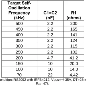
Choosing External Components Value
For suggested values of components for a given target self oscillating frequency, refer to Table 1. The OTA output has limited voltage and current compliances. These sets of components values are to ensure that OTA operates within its linear region so optimal THD+N performance can be achieved.
In case target frequency is somewhere in between the frequencies listed in the Table 1, adjust the frequency by tweaking R1, if necessary.
Target Self-Oscillation Frequency
(kHz)
C1=C2 (nF)
R1 (ohms)
500 2.2 200
450 2.2 165
400 2.2 141
350 2.2 124
300 2.2 115
250 2.2 102
200 4.7 41.2
150 10 20.0
100 10 14.0
70 22 4.42
Condition:IRS2092 with IRFB4212, Vbus=+/-35V, DT=25ns, RFB=47k.
Table 1 External Component Values vs. Self Oscillation Frequency
Clock Synchronization
In the typical PWM control loop design, the self-oscillating frequency can be set and
synchronized to an external clock. Through a set of resistor and a capacitor, the external clock injects periodic pulsating charges into the integrator, forcing oscillation to lock up to the external clock frequency. Typical setup with 5Vp-p 50% duty clock signal uses RCK=22k and
CCK=33pF in Figure 3. To maximize audio
performance, the self running frequency without clock injection should be 20 to 30% higher than the external clock frequency.
Vin
C1 C2 R1
RFB
RIN
+
COMP
GND
IN-EXT. CLK RCK CCK
Figure 3 External Clock Sync
Figure 4 shows how self-oscillating frequency locks up to an external clock frequency.
0 100 200 300 400 500 600
10% 20% 30% 40% 50% 60% 70% 80% 90%
Duty Cycle
O
p
er
at
in
g
F
re
q
u
en
c
y
(k
H
z)
Figure 4 Typical Lock Range to External Clock Click Noise Elimination
The IRS2092(S) has a unique feature that minimizes Turn-ON and -OFF audible click noise. When CSD is in between Vth1 and Vth2 during start up, an internal closed loop around the OTA enables an oscillation that generates voltages at COMP and IN-, bringing them to steady state values. It runs at around 1MHz, independent from the switching oscillation.
COMP PWM
Vin
C1 C2
R1
RFB
RIN
+
COMP
GND IN-C3
Cc
Start-up
As a result, all capacitive components connected to COMP and IN- pins, such as C1, C2, C3 and Cc in Figure 5, are pre-charged to their steady state values during the star up sequence. This allows instant settling of PWM operation.
To utilize the click noise reduction function, following conditions must be met.
1. CSD pin has slow enough ramp up from Vth1 to Vth2 such that the voltages in the capacitors can settle to their target values. 2. High side bootstrap power supply needs to be charged up prior to starting oscillation. 3. Audio input has to be zero.
4. For internal local loop to override external feedback during the startup period, DC offset at speaker output prior to shutdown release has to satisfy the following condition.
FB
R
A
DCoffset
<
30
m
×
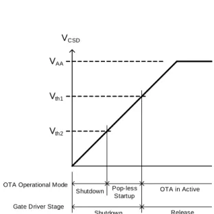
CSD Voltage and OTA Operational Mode
The CSD pin determines the operational mode of the IRS2092(S). The OTA has three operational modes; cut off, local oscillation and normal operation while the gate driver section has two modes; normal and shutdown with CSD voltage. When VCSD < Vth2, the IC is in shutdown mode and
the OTA is cut off.
When Vth2< VCSD < Vth1, the HO and LO outputs
are still in shutdown mode. The OTA is activated and starts local oscillation, which pre-biases all the capacitive components in the error amplifier. When VCSD>Vth1, shutdown is released and PWM
operation starts.
VCSD
VAA
Vth1
Vth2
Shutdown Release
OTA in Active Shutdown Pop-less
Startup Gate Driver Stage
OTA Operational Mode
Figure 6 VCSD and OTA Mode
Self-oscillation Start-up Condition
The IRS2092(S) requires the following
conditions to be met to start PWM oscillation in the typical application circuit.
- All the control power supplies, VAA, VSS, VCC and VBS are above the under voltage lockout thresholds. - CSD pin voltage is over Vth1 threshold. -
i
IN<
i
FBWhere
IN IN IN
R
V
i
=
,FB B FB
R
V
i
=
+.
Note that this condition also limits the maximum audio input voltage feeding into R1. If this condition is exceeded, the amplifier stops its oscillation during the operation period. This allows a 100% modulation index; however, a care should be taken so that the high side floating supply does not decay due to a lack of low side pulse ON state.
MOSFET Selection
There are a couple of limitations on size of MOSFET to be combined with the IRS2092(S).
1. Power dissipation
Power dissipation from gate driver stage in the IRS2092(S) is proportional to switching
frequency and gate charge of MOSFET. Higher the switching frequency the lower the gate charge that can be used.
Refer to Junction Temperature Estimation later in this application note for details.
2. Switching Speed
Internal over current protection has a certain time window to measure the output current. If switching transition takes too long, the internal OCP circuitry starts monitoring voltage across the MOSFET that induces false triggering of OCP. Less than 40nC of gate charge per output is recommended.
The IRS2092(S) accommodates a range of IR Digital Audio MOSFETs, providing a scalable design for various output power levels. For further
information on MOSFET section, refer to AN-1070, Class D Amplifier Performance Relationship to MOSFET Parameters.
Protection Design
Over Current Protection (OCP)
The IRS2092(S) features over current protection to protect the power MOSFETs during abnormal load conditions. The IRS2092(S) starts a sequence of events when it detects an over current condition during either high side or low side turn on of a pulse. As soon as either the high side or low side current sensing block detects over current:
1. The OC Latch (OCL) flips logic states and shutdowns the outputs LO and HO.
2. The CSD pin starts discharging the external capacitor Ct.
3. When VCSD, the voltage across Ct, falls
below the lower threshold Vth2, an output signal from COMP2 resets OCL.
4. The CSD pin starts charging the external capacitor Ct.
5. When VCSD goes above the upper threshold
Vth1, the logic on COMP1 flips and the IC resumes operation.
As long as the over current condition exists, the IC will repeat the over current protection sequence at a repetition rate dependent upon capacitance in CSD pin.
Vth1 Vth2 VSS VAA
tOCL/ tOCH
OC detection
CSD Capacitor
SD
tRESET
Protection reset interval Release
Shutdown Discharge
Charge
tSU
Power on mute Normal operation Normal operation
VCSD
VAA
`
`
CSD
VSS
S Q R COMP1
COMP2
HV LEVEL SHIFT
HV LEVEL SHIFT
UVLO(VB) OC DET (H)
HV LEVEL SHIFT
OC DET (L) UVLO(VCC)
OC
DEAD TIME SD
`
PWM HO LO
FLOATING HIGH SIDE FLOATING INPUT
LOW SIDE
Vth2 Vth1
Ct
Figure 8 Shutdown Functional Block Diagram Protection Control
The internal protection control block dictates the operational mode, normal or shutdown, using the input of the CSD pin. In shutdown mode, the IC forces LO and HO to output 0V with respect to COM and VS respectively to turn off the power MOSFETs. The CSD pin provides five functions.
1. Power up delay timer 2. Self-reset timer 3. Shutdown input
4. Latched protection configuration 5. Shutdown status output (host I/F) The CSD pin cannot be paralleled with other IRS2092(S).
Self Reset Protection
By putting a capacitor between CSD and VSS, the
IRS2092(S) resets itself after entering shutdown mode.
After the OCP event, CSD pin discharges Ct voltage VCSD down to the lower threshold Vth2 to reset the
internal shutdown latch. Then, the IRS2092(S) begins to charge Ct in an attempt to resume operation. Once the voltage of the CSD pin rises
VAA GND
IN-OCSET COM COMP VSS LO
VCC VREF
HO VS CSD
CSH VB
DT
2
16 1
4 3
5
6
7
8
15
14
13
12
11
10
9
Ct
Figure 9 Self Reset Protection Configuration Designing Ct
The timing capacitor, Ct, is used to program tRESET
and tSU.
· tRESET is the amount of time that elapses
from when the IC enters shutdown mode to the time when the IC resumes operation. tRESET should be long enough to avoid over
heating the MOSFETs from the repetitive sequence of shutting down and resuming operation during over current conditions. In most of the applications, the minimum recommended time for tRESET is 0.1 second.
· tSU is the amount of time between powering
up the IC in shutdown mode to the moment the IC releases shutdown to begin normal operation.
above the upper threshold, V normal operation.
The Ct determines tRESET and tSU as following equations: CSD DD RESET
I
V
Ct
t
×
×
=
1
.
1
[s]CSD DD SU
I
V
Ct
t
×
×
=
7
.
0
[s]where ICSD = the charge/discharge current at the
CSD pin
VDD = the floating input supply voltage with
respect to VSS.
Shutdown Input
The IRS2092(S) can be shut down by an external shutdown signal SD. Figure 10 shows how to add an external discharging path to shutdown the PWM.
VAA GND IN-OCSET COM COMP VSS LO VCC VREF HO VS CSD CSH VB DT 2 16 1 4 3 5 6 7 8 15 14 13 12 11 10 9 Ct SD
Figure 10 Shutdown Input Latched Protection
Connecting CSD to VDD through a 10k Ω or less
resistor configures the over current protection latch. The latch locks the IC in shutdown mode after over current is detected. An external reset switch can be used to bring CSD below the lower threshold Vth2 for a minimum of 200ns to properly reset the latch. After the power up sequence, a reset signal to the CSD pin is required to release the IC from the latched shutdown mode.
VAA GND IN-OCSET COM COMP VSS LO VCC VREF HO VS CSD CSH VB DT 2 16 1 4 3 5 6 7 8 15 14 13 12 11 10 9 SD <10k
Figure 11 Latched Protection with Reset Input Interfacing with System Controller
The IRS2092(S) can communicate with an external system controller through a simple interfacing circuit shown in Figure 12. A generic PNP transistor U1 detects the sink current at the CSD pin during an OCP event and outputs a shutdown signal to an external system controller. Another generic NPN transistor U2 can then reset the internal protection logic by pulling the CSD voltage below the lower threshold Vth2 for a minimum of 200ns. Note that the CSD pin is configured to operate in latched OCP. After the power up sequence, a reset signal to the CSD pin is required to release the IC from shutdown mode. VAA GND IN-OCSET COM COMP VSS LO VCC VREF HO VS CSD CSH VB DT 2 16 1 4 3 5 6 7 8 15 14 13 12 11 10 9 RESET <10k SD U1 U2
Figure 12 Interfacing with Host Controller Programming OCP Trip Level
In a Class D audio amplifier, the direction of the load current alternates with the audio input signal. An over-current condition can therefore occur during either a positive current cycle or a negative current cycle. The IRS2092(S) uses the RDS(on) of the output
MOSFETs as current sensing resistors. Due to the structural constraints of high voltage ICs, current sensing is implemented differently for the high side and low side. If the measured current exceeds a
HIGH SIDE CS
VB
HO
VS
LOW SIDE CS UV Q
UV DETECT DEAD TIME
VCC
LO
COM CSH
SD
OCSET
UV DETECT
HV LEVEL SHIFT HV
LEVEL SHIFT
FLOATING HIGH SIDE
5V REG
-B Vcc +B
OUT R1
R2
R3
D1
Q1
Q2
R4 R5
Dbs Cbs
VREF
Figure 13 Bi-directional Over Current Protection Low Side Over Current Sensing
For negative load currents, low side over current sensing monitors the load condition and shuts down switching operation if the load current exceeds the preset trip level.
Low side current sensing is based on the
measurement of VDS across the low side MOFET
during low side on state. In order to avoid triggering OCP from overshoot, a blanking interval inserted after LO turn on disables over current detection for 450ns.
The OCSET pin is to program the threshold for low side over current sensing. When the VDS measured
of the low side MOSFET exceeds the voltage at the OCSET pin with respect COM, the IRS2092(S) begins the OCP sequence described earlier.
Note that programmable OCSET range is 0.5V to 5.0V. To disable low side OCP, connect OCSET to VCC directly.
To program the trip level for over current, the voltage at OCSET can be calculated using the equation below.
VOCSET = VDS(LOW SIDE) = ITRIP+ x RDS(on)
In order to minimize the effect of the input bias current at the OCSET pin, select resistor values for R4 and R5 such that the current through the voltage divider is 0.5mA or more.
* Note: Using VREF to generate an input to OCSET
through a resistive divider provides improved immunity from fluctuations in VCC.
OC REF
OCREF
COM
OCSET
VS
OC
+
-IRS2092(S) OC Comparator R4
R5
-B +B
OUT Q1
Q2
LO LO
0.5mA 5.1V
Figure 14 Low Side Over Current Sensing
Low Side Over Current Setting
Let the low side MOSFET has RDS(on) of 100mΩ. We
wish to set the current trip level at 30A. VOCSET is given by:
VOCSET = ITRIP+ x RDS(on) = 30A x 100mW = 3.0V
Choose R4+R5=10 kW to properly load the VREF pin.
W =
W × =
W × =
k k V V
k V V R
REF OCSET
8 . 5
10 1 . 5
0 . 3
10 5
where VREF = 5.1V
Based on the E-12 series of resistor values, choose R5 to be 5.6kW and R4 to be 3.9kW to complete the design.
In general, RDS(on) has a positive temperature
coefficient that needs to be considered when setting the threshold level. Also, variations in RDS(on) will
affect the selection of external or internal component values.
High Side Over-Current Sensing
For positive load currents, high side over current sensing also monitors the load condition and shuts
High side current sensing is based on the
measurement of VDS across the high side MOSFET
during high side turn on through pins CSH and Vs. In order to avoid triggering OCP from overshoot, a blanking interval inserted after HO turn on disables over current detection for 450ns.
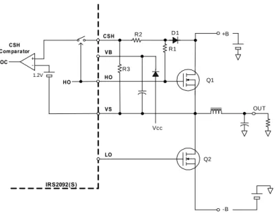
In contrast to low side current sensing, the threshold at which the CSH pin engages OC protection is internally fixed at 1.2V. An external resistive divider R2 and R3 can be used to program a higher threshold.
An external reverse blocking diode, D1, is required to block high voltages from feeding into the CSH pin while the high side is off.Due to a forward voltage drop of 0.6V across D1, the minimum threshold required for high side over current protection is 0.6V.
(
( ) (1))
3 2
3
D F HIGHSIDE DS
CSH V V
R R
R
V × +
+ =
where VDS(HIGH SIDE) = the drain to source voltage of
the high side MOSFET during high side turn on VF(D1) = the forward drop voltage of D1
Since VDS(HIGH SIDE) is determined by the product of
drain current ID and RDS(on) of the high side
MOSFET. VCSH can be rewritten as:
(
( ) ( 1))
3 2
3
D F D ON DS
CSH R I V
R R
R
V × × +
+ =
VS OC +
-IRS2092(S)
CSH Comparator
-B +B
OUT Q1
Q2
HO
LO HO
R1 R2 R3
D1
VB CSH
Vcc
1.2V
Figure 15 Programming High Side Over Current Threshold High Side Over Current Setting
Figure 15 demonstrates the typical circuitry used for high side current sensing. In the following example, the over current protection level is set to trip at 30A using a MOSFET with an RDS(on) of 100mW. The
component values of R2 and R3 can be calculated using the following formula:
Let R2 + R3=10 kW.
F DS
OCH
V V
Vth k R
+ × W =10
3
where VthOCL = 1.2V
VF = the forward voltage of reverse blocking
diode D1 = 0.6V.
VDS@ID=30A = the voltage drop across the
high side MOSFET when the MOSFET current is 30A.
Therefore, VDS@ID=30A = ID x RDS(on) = 30A x 100mW =
3V
Based on the formulas above, R2 = 6.8kW and R3 = 3.3kW.
Choosing the Correct Right Reverse Blocking Diode
The selection of the appropriate reverse blocking diode D1 depends on its voltage rating and speed. To effectively block bus voltages, the reverse voltage must be higher than the voltage difference
between +B and –B and the reverse recovery time must be as fast as the boot strap charging diode. A diode such as the Philips BAV21W, a 200V, 50ns high speed switching diode, is more than sufficient.
Dead-Time Generator
Dead-time is the blanking period inserted between either high-side Turn-OFF and low-side Turn-ON, or low-side Turn-OFF and high-side Turn-ON. Its purpose is to prevent shoot through, or a rush of current through both MOSFETs. In the IRS2092(S), an internal dead-time generation block allows the user to select the optimum dead time from a range of preset values. Selecting a preset dead-time through the DT/SD pin voltage can easily be done through an external voltage divider. This way of setting dead-time prevents outside noise from modulating the switching timing, which is critical to the audio performance.
How to Determine Optimal Dead-Time
The effective dead-time in an actual application differs from the dead-time specified in this datasheet due to the switching fall time, tf. The dead-time value in this datasheet is defined as the time period between the beginning of turn-off on one side of the switching stage and the beginning of turn-on on the other side as shown in Figure 16. The fall time of the MOSFET gate voltage must be subtracted from the dead-time value in the datasheet to determine the effective dead-time of a Class D audio amplifier.
(Effective dead-time) = (Dead-time in datasheet) – tf
HO (or LO)
LO (or HO)
tf
Dead-time in datasheet
Effective dead - time
10% 10%
90%
Figure 16 Effective Dead Time
A longer dead-time period is required for a MOSFET with a larger gate charge value because of the longer tf. Although a shorter effective dead-time setting is beneficial to achieving better linearity in Class D amplifiers, the likelihood of shoot-through current increases with narrower dead-time settings. Negative values of effective dead-time may cause excessive heat dissipation in the MOSFETs, leading to potentially serious damage.
To calculate the optimal dead-time in a given application, the fall time tf for both HO and LO in the actual circuit need to be taken into account. In addition, variations in temperature and device parameters could also affect the effective dead-time in the actual circuit. Therefore, a minimum effective dead-time of 10ns is recommended to avoid shoot-through current over the range of operating temperatures and supply voltages.
Programming Dead-Time
The IRS2092(S) selects the dead-time from a range of preset dead-time values based on the voltage applied at the DT pin. An internal comparator translates the DT input to a predetermined dead-time by comparing the input with internal reference voltages. These internal reference voltages are set in the IC through a resistive voltage divider using VCC. The relationship between the operation mode
and the voltage at DT pin is illustrated in the Figure17 below.
Vcc 0.57xVcc
0.36xVcc 0.23xVcc 105nS
75nS 45nS 25nS
VDT
Dead-time
Figure 17 Dead Time vs. VDT
Table 3 suggests pairs of resistor values used in the voltage divider for selecting dead-time. Resistors with up to 5% tolerance are acceptable when using these values.
Vcc
COM DT
>0.5mA
R1 R2
IRS2092(S)
Figure 18 External Voltage Divider
Dead-time Mode R1 R2 DT/SD Voltage
DT1 <10k Open Vcc
DT2 5.6kW 4.7kW 0.46 x Vcc
DT3 8.2kW 3.3kW 0.29 x Vcc
DT4 Open <10k COM
Supplying VAA and VSS
There are two ways to implement power supplies VAA and VSS.
1. Supplying VAA and VSS with External
Regulators
For best audio performance, it is preferred to produce VAA and VSS with external regulators, such
as the three terminal regulators. To keep internal clamping zener diodes from conducting, the supply voltage should be VAA < VCLAMPM+ and VSS > V
CLAMPM-. Standard 7805 and 7905 regulators are suitableCLAMPM-.
7805 7905 VAA GND IN-OCSET COM COMP VSS LO VCC VREF HO VS CSD CSH VB DT 2 16 1 4 3 5 6 7 8 15 14 13 12 11 10 9
Figure 19 Supplying VAA and VSS with External
Regulators
When switched mode regulators provide VAA and
VSS, it is required to place a two stage noise filter in
the supply lines as shown in Figure 20 to prevent noise from influencing the switching ripple voltage on +/-5V. IRS2092(S) VAA GND IN-OCSET COM COMP VSS LO VCC VREF HO VS CSD CSH VB DT 2 16 1 4 3 5 6 7 8 15 14 13 12 11 10 9 10nF 10µF
10µF 2.2µF 2.2µF 10 10 10 10 +5V -5V
Figure 20 Supplying VAA and VSS from Switched
ModePower Supply
2. Regulating VAA and VSS Using Internal
Zener Diodes
VAA and VSS can be supplied with an internal zener
diode clamp as a shunt regulator. Recommended
IAA and ISS, the supply current for VAA and VSS, is
10mA.
This implementation is suggested when the main bus voltages, +B and –B, are supplied from a regulated power supply.
Set RAA and RSS values in Figure 21 such that the
supply currents feeding into VAA and VSS are each
10mA. VAA GND IN -OCSET COM COM P VSS L O
VC C VREF HO VS C SD CSH VB -B +B D T 2 16 1 4 3 5 6 7 8 15 14 13 12 11 10 9 RAA RSS
Figure 21 Regulating VAA and VSS with Internal
Zener Diodes
Charging VBS Prior to Start
For proper start-up, the high side bootstrap capacitor is required to be charged prior to PWM start-up through a resistor RCHARGE from the positive
supply bus to the VB pin. By utilizing an internal
20.8V zener diode between VB and VS, this scheme
eliminates the need to charge the boot strap capacitor through low side turn on during start up. The value of this charging resistor is subject to several constraints:
- The minimum resistance of RCHARGE is
limited by the maximum PWM modulation index of the system. When HO is high, RCHARGE drains bootstrap power supply so it
reduces holding up time, hence maximum continuous HO on time.
- The maximum resistance of RCHARGE is
limited by the current charge capability of the resistor during startup:
QBS
CHARGE I
I >
where ICHARGE = the current through
RCHARGE
IQBS = the high side supply
ICHARGE generates a DC offset at the speaker output
prior to PWM start up. Check that the DC offset does not exceed a condition for click noise
elimination. See Click Noise Elimination section for more detail.
12V -B Vcc +B Rcharge
VAA
GND
IN-OCSET COM COMP
VSS LO
VCC
VREF HO
VS
CSD
CSH
VB
DT
2
16 1
4 3
5 6 7 8
15 14 13 12 11 10 9
Figure 22 Boot Strap Supply Pre-charging Start-up Sequence (UVLO)
The protection control block in the IRS2092(S) monitors the status of VAA and VCC to ensure that
both voltage supplies are above their respective UVLO (Under Voltage Lock Out) thresholds before beginning normal operation. If either VAA or VCC is
below the under voltage threshold, LO and HO are disabled in shutdown mode until both VAA and VCC
rise above their voltage thresholds.
Power-down Sequence
As soon as VAA or VCC falls below its UVLO
threshold, protection logic in the IRS2092(S) turns off LO and HO, shutting off the power MOSFETs.
U VLO ( VCC ) VCC
HO
LO
Figure 23 IRS2092(S) UVLO Timing Chart Power Supply Decoupling
Careful attention must be given to decoupling the power supplies for proper operation of the IC. Ceramic capacitors of 0.1µF or more should be placed close to the power supply pins of the IC on the board.
VSS Negative Bias Clamping
An excessive negative Vss voltage with respect to COM could damage the IRS2092(S). VSS can go
below COM when a negative supply is missing in a dual supply configuration. To protect the IC from this possibility, a diode is recommended for clamping potential negative biases to VSS. A standard
recovery diode with a current rating of 1A such as the 1N4002 is sufficient for this purpose.
VAA GND
IN-OCSET COM COM P VSS L O
VCC VREF
HO VS CSD
C SH VB
D T
2
16 1
4 3
5 6 7 8
15 14 13 12 11 10 9
-B
Figure 24 Negative VSS Clamping
Junction Temperature Estimation
The power dissipation in the IRS2092(S) is dominated by the following items:
- PMID: Power dissipation of the input floating
logic and protection circuitry
- PLSM: Power dissipation of the Input Level
Shifter
- PLOW: Power dissipation in low side
- PLSH: Power dissipation of the High-side
Level Shifter
- PHIGH: Power dissipation in high side
The following equations are for your reference only. Because of the non-linear characteristics in gate drive stage, these assumptions may not be accurate.
1. PMID: Power Dissipation of the Input
Floating Logic and Protection Circuitry
The power dissipation of the input floating section is given by:
OTA ZENER
MID P P
P = +
POTA = the power dissipation from the
internal OTA
When VAA and VSS are regulated with internal
zener diode clamping, PMID can be simplified as:
(
) (
) (
)
SS AA BUS SS AA BUS SS AA MID R R V V V V V V P + -+ -× -» + -WhereV+BUS = positive bus voltage feeding
VAA
V-BUS = negative bus voltage feeding
VSS
RAA = resistor feeding VAA from V+BUS
RSS = resistor feeding VSS from
V-BUS
See Figure 21.
2. PLSM: Power Dissipation of the Input
Level Shifter
PLSM = 1.5 x 10⁻⁹ x fSW x VSS BIAS
Where
fSW = the PWM switching frequency
VSS BIAS = the bias voltage of VSS
with respect to COM
3. PLOW: Power Dissipation of Low Side The power dissipation of the low side comes from the losses of the logic circuitry and the losses of driving LO.
(
)
÷÷ ø ö ç ç è æ + + × × × + × = + = (int) g g O O SW g CC QCC LO LDD LOW R R R R f Q Vcc V I P P P WherePLDD = power dissipation of the
internal logic circuitry
PLO = power dissipation from of gate
drive stage for LO
RO = output impedance of LO,
typically 10 Ω for the IRS2092(S)
Rg(int) = internal gate resistance of the
low side MOSFET, typically 2Ω Rg = external gate resistance of the
low side MOSFET
Qg = total gate charge of the low side MOSFET
4. PLSH: Power Dissipation of the High-side
Level Shifter
PLSH = 0.4nC x fsw x VBUS
Where
fSW = PWM switching frequency
VBUS = difference between the positive
bus voltage and negative bus voltage
5. PHIGH: Power Dissipation of High Side The power dissipation of the high side comes from the losses of the logic circuitry and the losses of driving HO.
(
)
÷÷ ø ö ç ç è æ + + × × × + × = + = (int) g g O O SW g BS BS QBS HO LDD HIGH R R R R f Q V V I P P P WherePLDD = power dissipation of the
internal logic circuitry
PHO = power dissipation of the gate
drive stage for HO
RO = equivalent output impedance of
HO, typically 10 Ω for the IRS2092(S) Rg(int) = the internal gate resistance of
the high side MOSFET, typically 2Ω
Rg = external gate resistance of the
high side MOSFET
Qg = total gate charge of the high side MOSFET
6. PD: Total Power Dissipation Total power dissipation, PD, is given by
HIGH HSM LOW LSM MID
D P P P P P
P = + + + + .
7. Tj: Junction Temperature
Given junction to ambient thermal resistance RthJA,
the junction temperature Tjcan be calculated from the formula provided below and must not exceed 150°C.
C T
P Rth
TJ = JA× d+ A<150°
Board Layout Considerations
The floating input section of the IRS2092(S) consists of a low noise OTA error amplifier and a PWM comparator along with CMOS logic circuitry. High frequency bypass capacitor CVAA-VSS should be
placed closest to the IRS2092(S) to supply the logic circuitry. CVAA and CVSS are for stable operation of
the OTA and should be placed close to the IC. Gate driver supply capacitors CVCC and CVBS provide
gate charging current and should also be placed close to the IRS2092(S).
IRS2092(S)
VAA GND
IN-OCSET COM COMP VSS LO
VCC VREF
HO VS CSD
CSH VB
DT
2
16 1
4 3
5 6 7 8
15 14 13 12 11 10 9
CVAA
CVSS
CVBS
CVCC
CVAA-VSS
Figure 25 Placement Sensitive Bypass Capacitors
Ground Plane
In addition to the key component locations mentioned above, it is important to properly pour
plane design because the integration of circuitries within the IC is referenced to different potentials. Proper application of the IRS2092(S) employs three reference potentials.
1. Analog Ground
The Input analog section around the OTA is referenced to the signal ground, or GND, which should be a quiet reference node for the audio input signal. The peripheral circuits in the floating input section such as CSD and COM pins refer to this ground. These nodes should all be separate from the switching stages of the system. In order to prevent potential capacitive coupling to the
switching nodes, use a ground plane only in this part of the circuit. Do not share the ground plane with gate driver or power stages.
2. Gate Driver Reference
The gate driver stage of the IRS2092(S) is located between pins 10 and 15 and is referenced to the negative bus voltage, COM. This is the substrate of the IC and acts as ground. Although the negative bus is a noisy node in the system, both of the gate drivers refer to this node. Therefore, it is important to shield the gate drive stages with the negative bus voltage so that all the noise currents due to stray capacitances flow back to the power supply without degrading signal ground.
3. Power Ground
Power ground is the ground connection that closes the loops of the bus capacitors and inductor ripple current circuits. Separate the power ground and input signal grounds from each other as much as possible to avoid common stray impedances. Figure 26 illustrates how to paint out reference planes. Power GND plane should include negative bus cap. Power reference plane should include Vcc. Also, Use distinctly different symbols for the different grounds.
AN-Figure 26 Applying Ground Planes