MC10EP446, MC100EP446
3.3 V/5 V 8‐Bit
CMOS/ECL/TTL Data Input
Parallel/Serial Converter
Description
The MC10/100EP446 is an integrated 8−bit parallel to serial data
converter. The device is designed with unique circuit topology to
operate for NRZ data rates up to 3.2 Gb/s. The conversion sequence
from parallel data into a serial data stream is from bit D0 to D7. The
parallel input pins D0−D7 are configurable to be threshold controlled by
CMOS, ECL, or TTL level signals. The serial data rate output can be
selected at internal clock data rate or twice the internal clock data rate
using the CKSEL pin.
Control pins are provided to reset (SYNC) and disable internal clock
circuitry (CKEN). In either CKSEL modes, the internal flip−flops are
triggered on the rising edge for CLK and the multiplexers are switched
on the falling edge of CLK, therefore, all associated specification
limits are referenced to the negative edge of the clock input.
Additionally, V
BBpin is provided for single−ended input condition.
The 100 Series devices contain temperature compensation network.
Features•
3.2 Gb/s Typical Data Rate Capability
•
Differential Clock and Serial Outputs
•
V
BBOutput for Single-ended Input Applications
•
Asynchronous Data Reset (SYNC)
•
PECL Mode Operating Range:
V
CC= 3.0 V to 5.5 V with V
EE= 0 V
•
NECL Mode Operating Range:
V
CC= 0 V with V
EE= −3.0 V to −5.5 V
•
Open Input Default State
•
Safety Clamp on Inputs
•
Parallel Interface Can Support PECL, TTL or CMOS
•
These Devices are Pb−Free and are RoHS Compliant
http://onsemi.com
See detailed ordering and shipping information in the package dimensions section on page 18 of this data sheet.
ORDERING INFORMATION LQFP−32
FA SUFFIX CASE 873A
MARKING DIAGRAM*
*For additional marking information, refer to Application Note AND8002/D.
xxx = 10 or 100 A = Assembly Location WL = Wafer Lot YY = Year WW = Work Week G or G = Pb−Free Package
MCxxx EP446 AWLYYWWG
QFN32 MN SUFFIX CASE 488AM
32
1 MCxxx
EP446 AWLYYWWG
G
1
25 26 27 28 29 30 31 32
15 14 13 12 11 10 9
1 2 3 4 5 6 7 8
24 23 22 21 20 19 18 17 16
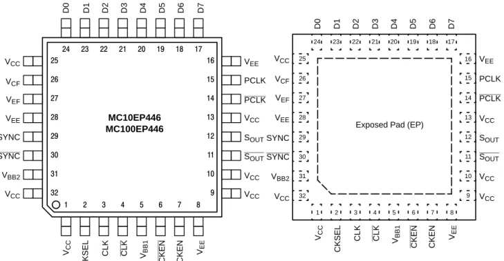
Figure 1. LQFP−32 Pinout (Top View)
Warning: All VCC and VEE pins must be externally connected to Power Supply to guarantee proper operation.
D0 D1 D3 D4 D7
VCC
SOUT VEE
VBB2
VCC
CKSEL
VEF
VEE
PCLK PCLK
D2 D5 D6
SOUT VCF
SYNC SYNC
VCC
CLK CLK VBB1 CKEN CKEN
VEE
VCC
VCC
VCC
MC10EP446 MC100EP446
Figure 2. QFN−32 Pinout (Top View)
32 31 30 29 28 27 26 25
9 10 11 12 13 14 15 16
1 2 3 4 5 6 7 8
24 23 22 21 20 19 18 17
Exposed Pad (EP)
D0 D1 D3 D4 D7
VCC
CKSEL
D2 D5 D6
CLK CLK VBB1 CKEN CKEN
VEE
SOUT VEE
PCLK PCLK
SOUT VCC
VCC
VCC VCC
VEE
VBB2 VEF VCF
SYNC SYNC
VCC
Table 1. PIN DESCRIPTION
PIN FUNCTION
D0*−D7* ECL, CMOS, or TTL Parallel Data Input SOUT, SOUT ECL Differential Serial Data Output
CLK*, CLK* ECL Differential Clock Input
PCLK, PCLK ECL Differential Parallel Clock Output
SYNC*, SYNC** ECL Conversion Synchronizing Differential Input (Reset)***
CKSEL* ECL Clock Input Selector
CKEN*, CKEN* ECL Clock Enable Differential Input
VCF ECL, CMOS, or TTL Input Selector
VEF ECL Reference Mode Connection
VBB1,VBB2 Reference Voltage Output
VCC Positive Supply
VEE Negative Supply
* Pins will default LOW when left open. **Pins will default HIGH when left open.
***The rising edge of SYNC will asynchronously reset the internal circuitry. The falling edge of the SYNC followed by the falling edge of CLK initiates the conversion process synchronously on the next rising edge of CLK.
Table 2. TRUTH TABLE
Pin
Function
HIGH LOW
CKSEL
SOUT: PCLK = 8:1 CLK: SOUT = 1:1
SOUT CLK
SOUT: PCLK = 8:1 CLK: SOUT = 1:2
SOUT CLK
CKEN Synchronously Disables Normal Parallel to Serial Conversion
Synchronously Enables Normal Parallel to Serial Conversion
SYNC Asynchronously Resets Internal Flip−Flops* Synchronous Enable
*The rising edge of SYNC will asynchronously reset the internal circuitry. The falling edge of the SYNC followed by the falling edge of CLK initiates the conversion process synchronously on the next rising edge of CLK.
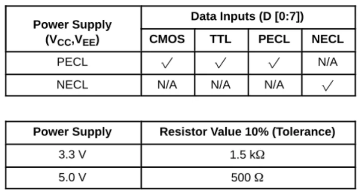
Table 3. INPUT VOLTAGE LEVEL SELECTION TABLE
Input Function Connect To VCF Pin
ECL Mode VEF Pin
CMOS Mode No Connect
TTL Mode* 1.5 V $ 100 mV
*For TTL Mode, if no external voltage can be provided, the reference voltage can be provided by connecting the appropriate resistor between VCF and VEE pins.
Table 4. DATA INPUT OPERATING VOLTAGE TABLE Power Supply
(VCC,VEE)
Data Inputs (D [0:7])
CMOS TTL PECL NECL
PECL p p p N/A
NECL N/A N/A N/A p
Power Supply Resistor Value 10% (Tolerance)
3.3 V 1.5 kW
SYNC
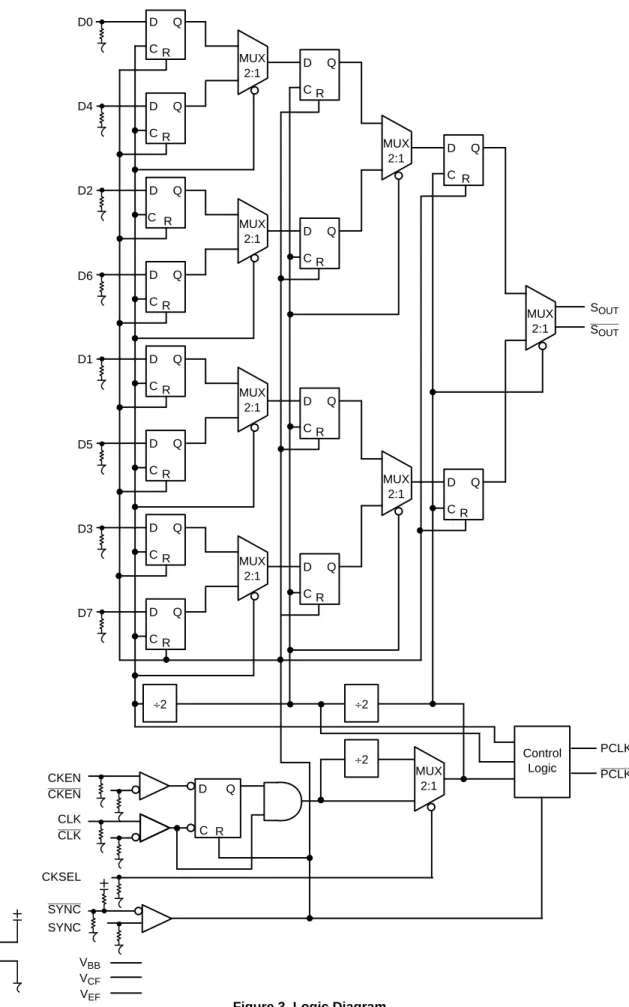
Figure 3. Logic Diagram
D0 D Q
R C
D Q R C D4
D Q R C
D Q R C
D Q R C
D Q R C
D Q R C
D Q R C D2
D6
D1
D5
D3
D7
MUX 2:1
MUX 2:1
MUX 2:1
MUX 2:1
D Q R C
D Q R C
D Q R C
D Q R C
÷2
MUX 2:1
MUX 2:1
D Q R C
D Q R C
MUX 2:1
÷2
÷2
D Q
R C
SOUT SOUT
PCLK PCLK MUX
2:1 CKEN
CKEN CLK CLK
CKSEL
SYNC VBB VCF VEF VEE
Control Logic
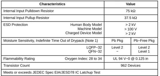
Table 5. ATTRIBUTES
Characteristics Value
Internal Input Pulldown Resistor 75 kW
Internal Input Pullup Resistor 37.5 kW
ESD Protection Human Body Model Machine Model Charged Device Model
> 2 kV > 100 V
> 2 kV
Moisture Sensitivity, Indefinite Time Out of Drypack (Note 1) Pb Pkg Pb−Free Pkg LQFP−32
QFN−32
Level 2 −
Level 2 Level 1 Flammability Rating Oxygen Index: 28 to 34 UL 94 V−0 @ 0.125 in
Transistor Count 962 Devices
Meets or exceeds JEDEC Spec EIA/JESD78 IC Latchup Test 1. For additional information, see Application Note AND8003/D.
Table 6. MAXIMUM RATINGS
Symbol Parameter Condition 1 Condition 2 Rating Unit
VCC PECL Mode Power Supply VEE = 0 V 6 V
VEE NECL Mode Power Supply VCC = 0 V −6 V
VI PECL Mode Input Voltage NECL Mode Input Voltage
VEE = 0 V VCC = 0 V
VI≤ VCC VI≥ VEE
6 −6
V
Iout Output Current Continuous
Surge
50 100
mA
IBB VBB Sink/Source ± 0.5 mA
TA Operating Temperature Range −40 to +85 °C
Tstg Storage Temperature Range −65 to +150 °C
qJA Thermal Resistance (Junction−to−Ambient) 0 lfpm 500 lfpm
LQFP−32 LQFP−32
80 55
°C/W
qJC Thermal Resistance (Junction−to−Case) Standard Board LQFP−32 12 to 17 °C/W qJA Thermal Resistance (Junction−to−Ambient) 0 lfpm
500 lfpm
QFN−32 QFN−32
31 27
°C/W
qJC Thermal Resistance (Junction−to−Case) 2S2P QFN−32 12 °C/W
Tsol Wave Solder Pb−Free <2 to 3 sec @ 260°C 265 °C
Stresses exceeding those listed in the Maximum Ratings table may damage the device. If any of these limits are exceeded, device functionality should not be assumed, damage may occur and reliability may be affected.
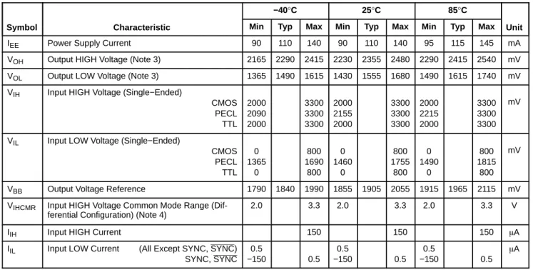
Table 7. 10EP DC CHARACTERISTICS, PECL VCC = 3.3 V, VEE = 0 V (Note 2)
Symbol Characteristic
−40°C 25°C 85°C
Unit
Min Typ Max Min Typ Max Min Typ Max
IEE Power Supply Current 90 110 140 90 110 140 95 115 145 mA
VOH Output HIGH Voltage (Note 3) 2165 2290 2415 2230 2355 2480 2290 2415 2540 mV
VOL Output LOW Voltage (Note 3) 1365 1490 1615 1430 1555 1680 1490 1615 1740 mV
VIH Input HIGH Voltage (Single−Ended)
CMOS PECL TTL
2000 2090 2000
3300 3300 3300
2000 2155 2000
3300 3300 3300
2000 2215 2000
3300 3300 3300
mV
VIL Input LOW Voltage (Single−Ended)
CMOS PECL TTL
0 1365
0
800 1690
800 0 1460
0
800 1755
800 0 1490
0
800 1815
800 mV
VBB Output Voltage Reference 1790 1840 1990 1855 1905 2055 1915 1965 2115 mV
VIHCMR Input HIGH Voltage Common Mode Range (Dif-ferential Configuration) (Note 4)
2.0 3.3 2.0 3.3 2.0 3.3 V
IIH Input HIGH Current 150 150 150 mA
IIL Input LOW Current (All Except SYNC, SYNC) SYNC, SYNC
0.5
−150 0.5
0.5
−150 0.5
0.5
−150 0.5
mA NOTE: Device will meet the specifications after thermal equilibrium has been established when mounted in a test socket or printed circuit
board with maintained transverse airflow greater than 500 lfpm. Electrical parameters are guaranteed only over the declared operating temperature range. Functional operation of the device exceeding these conditions is not implied. Device specification limit values are applied individually under normal operating conditions and not valid simultaneously.
2. Input and output parameters vary 1:1 with VCC. VEE can vary +0.3 V to −2.2 V. 3. All loading with 50 W to VCC − 2.0 V.
4. VIHCMR min varies 1:1 with VEE, VIHCMR max varies 1:1 with VCC. The VIHCMR range is referenced to the most positive side of the differential input signal.
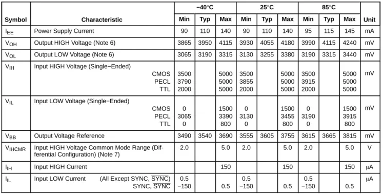
Table 8. 10EP DC CHARACTERISTICS, PECL VCC = 5.0 V, VEE = 0 V (Note 5)
Symbol Characteristic
−40°C 25°C 85°C
Unit
Min Typ Max Min Typ Max Min Typ Max
IEE Power Supply Current 90 110 140 90 110 140 95 115 145 mA
VOH Output HIGH Voltage (Note 6) 3865 3950 4115 3930 4055 4180 3990 4115 4240 mV
VOL Output LOW Voltage (Note 6) 3065 3190 3315 3130 3255 3380 3190 3315 3440 mV
VIH Input HIGH Voltage (Single−Ended)
CMOS PECL TTL
3500 3790 2000
5000 5000 5000
3500 3855 2000
5000 5000 5000
3500 3915 2000
5000 5000 5000
mV
VIL Input LOW Voltage (Single−Ended)
CMOS PECL TTL
0 3065
0
1500 3390 800
0 3130
0
1500 3455 800
0 3190
0
1500 3915 800
mV
VBB Output Voltage Reference 3490 3540 3690 3555 3605 3755 3615 3665 3815 mV
VIHCMR Input HIGH Voltage Common Mode Range (Dif-ferential Configuration) (Note 7)
2.0 5.0 2.0 5.0 2.0 5.0 V
IIH Input HIGH Current 150 150 150 mA
IIL Input LOW Current (All Except SYNC, SYNC) SYNC, SYNC
0.5
−150 0.5
0.5
−150 0.5
0.5
−150 0.5
mA NOTE: Device will meet the specifications after thermal equilibrium has been established when mounted in a test socket or printed circuit
board with maintained transverse airflow greater than 500 lfpm. Electrical parameters are guaranteed only over the declared operating temperature range. Functional operation of the device exceeding these conditions is not implied. Device specification limit values are applied individually under normal operating conditions and not valid simultaneously.
5. Input and output parameters vary 1:1 with VCC. VEE can vary +2.0 V to −0.5 V. 6. All loading with 50 W to VCC − 2.0 V.
7. VIHCMR min varies 1:1 with VEE, VIHCMR max varies 1:1 with VCC. The VIHCMR range is referenced to the most positive side of the differential input signal.
Table 9. 10EP DC CHARACTERISTICS, NECL VCC = 0 V, VEE = −5.5 V to −3.0 V (Note 8)
Symbol Characteristic
−40°C 25°C 85°C
Unit
Min Typ Max Min Typ Max Min Typ Max
IEE Power Supply Current 90 110 140 90 110 140 95 115 145 mA
VOH Output HIGH Voltage (Note 9) −1135 −1010 −885 −1070 −945 −820 −1010 −885 −760 mV
VOL Output LOW Voltage (Note 9) −1935 −1810 −1685 −1870 −1745 −1620 −1810 −1685 −1560 mV
VIH Input HIGH Voltage (Single−Ended) −1210 −885 −1145 −820 −1085 −760 mV
VIL Input LOW Voltage (Single−Ended) −1935 −1610 −1870 −1545 −1810 −1485 mV
VBB Output Voltage Reference −1510 −1460 −1310 −1445 −1395 −1245 −1385 −1335 −1185 mV
VIHCMR Input HIGH Voltage Common Mode Range (Differential Configuration) (Note 10)
VEE+2.0 0.0 VEE+2.0 0.0 VEE+2.0 0.0 V
IIH Input HIGH Current 150 150 150 mA
IIL Input LOW Current
(All Except SYNC, SYNC) SYNC, SYNC
0.5
−150 0.5
0.5
−150 0.5
0.5
−150 0.5
mA
NOTE: Device will meet the specifications after thermal equilibrium has been established when mounted in a test socket or printed circuit board with maintained transverse airflow greater than 500 lfpm. Electrical parameters are guaranteed only over the declared operating temperature range. Functional operation of the device exceeding these conditions is not implied. Device specification limit values are applied individually under normal operating conditions and not valid simultaneously.
8. Input and output parameters vary 1:1 with VCC. 9. All loading with 50 W to VCC − 2.0 V.
10. VIHCMR min varies 1:1 with VEE, VIHCMR max varies 1:1 with VCC. The VIHCMR range is referenced to the most positive side of the differential input signal.
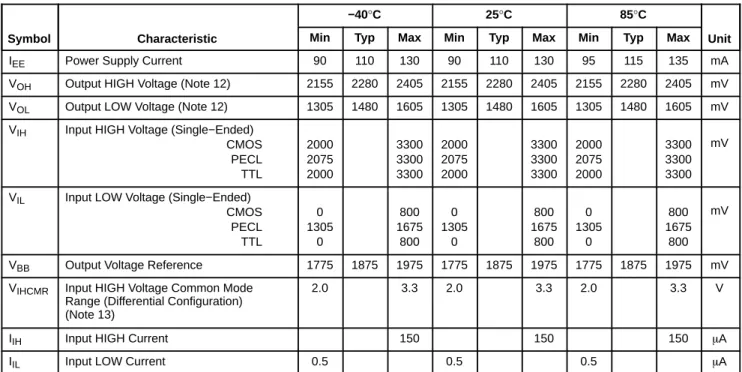
Table 10. 100EP DC CHARACTERISTICS, PECL VCC = 3.3 V, VEE = 0 V (Note 11)
Symbol Characteristic
−40°C 25°C 85°C
Unit
Min Typ Max Min Typ Max Min Typ Max
IEE Power Supply Current 90 110 130 90 110 130 95 115 135 mA
VOH Output HIGH Voltage (Note 12) 2155 2280 2405 2155 2280 2405 2155 2280 2405 mV
VOL Output LOW Voltage (Note 12) 1305 1480 1605 1305 1480 1605 1305 1480 1605 mV
VIH Input HIGH Voltage (Single−Ended) CMOS
PECL TTL
2000 2075 2000
3300 3300 3300
2000 2075 2000
3300 3300 3300
2000 2075 2000
3300 3300 3300
mV
VIL Input LOW Voltage (Single−Ended) CMOS
PECL TTL
0 1305
0
800 1675
800 0 1305
0
800 1675
800 0 1305
0
800 1675
800 mV
VBB Output Voltage Reference 1775 1875 1975 1775 1875 1975 1775 1875 1975 mV
VIHCMR Input HIGH Voltage Common Mode Range (Differential Configuration) (Note 13)
2.0 3.3 2.0 3.3 2.0 3.3 V
IIH Input HIGH Current 150 150 150 mA
IIL Input LOW Current 0.5 0.5 0.5 mA
NOTE: Device will meet the specifications after thermal equilibrium has been established when mounted in a test socket or printed circuit board with maintained transverse airflow greater than 500 lfpm. Electrical parameters are guaranteed only over the declared operating temperature range. Functional operation of the device exceeding these conditions is not implied. Device specification limit values are applied individually under normal operating conditions and not valid simultaneously.
11. Input and output parameters vary 1:1 with VCC. VEE can vary +0.3 V to −2.2 V. 12. All loading with 50 W to VCC − 2.0 V.
13. VIHCMR min varies 1:1 with VEE, VIHCMR max varies 1:1 with VCC. The VIHCMR range is referenced to the most positive side of the differential input signal.
Table 11. 100EP DC CHARACTERISTICS, PECL VCC = 5.0 V, VEE = 0 V (Note 14)
Symbol Characteristic
−40°C 25°C 85°C
Unit
Min Typ Max Min Typ Max Min Typ Max
IEE Power Supply Current 90 110 130 90 110 130 95 115 135 mA
VOH Output HIGH Voltage (Note 15) 3855 3980 4105 3855 3980 4105 3855 3980 4105 mV
VOL Output LOW Voltage (Note 15) 3005 3180 3305 3005 3180 3305 3005 3180 3305 mV
VIH Input HIGH Voltage (Single−Ended) CMOS
PECL TTL
3500 3775 2000
5000 5000 5000
3500 3775 2000
5000 5000 5000
3500 3775 2000
5000 5000 5000
mV
VIL Input LOW Voltage (Single−Ended) CMOS
PECL TTL
0 3005
0
1500 3375 800
0 3005
0
1500 3375 800
0 3005
0
1500 3375 800
mV
VBB Output Voltage Reference 3475 3575 3675 3475 3575 3675 3475 3575 3675 mV
VIHCMR Input HIGH Voltage Common Mode Range (Differential Configuration) (Note 16)
2.0 5.0 2.0 5.0 2.0 5.0 V
IIH Input HIGH Current 150 150 150 mA
IIL Input LOW Current 0.5 0.5 0.5 mA
NOTE: Device will meet the specifications after thermal equilibrium has been established when mounted in a test socket or printed circuit board with maintained transverse airflow greater than 500 lfpm. Electrical parameters are guaranteed only over the declared operating temperature range. Functional operation of the device exceeding these conditions is not implied. Device specification limit values are applied individually under normal operating conditions and not valid simultaneously.
14. Input and output parameters vary 1:1 with VCC. VEE can vary +2.0 V to −0.5 V. 15. All loading with 50 W to VCC − 2.0 V.
16. VIHCMR min varies 1:1 with VEE, VIHCMR max varies 1:1 with VCC. The VIHCMR range is referenced to the most positive side of the differential input signal.
Table 12. 100EP DC CHARACTERISTICS, NECL VCC = 0 V, VEE = −5.5 V to −3.0 V (Note 17)
Symbol Characteristic
−40°C 25°C 85°C
Unit
Min Typ Max Min Typ Max Min Typ Max
IEE Power Supply Current 90 110 130 90 110 130 95 115 135 mA
VOH Output HIGH Voltage (Note 18) −1145 −1020 −895 −1145 −1020 −895 −1145 −1020 −895 mV
VOL Output LOW Voltage (Note 18) −1995 −1820 −1695 −1995 −1820 −1695 −1995 −1820 −1695 mV
VIH Input HIGH Voltage (Single−Ended) −1225 −880 −1225 −880 −1225 −880 mV
VIL Input LOW Voltage (Single−Ended) −1995 −1625 −1995 −1625 −1995 −1625 mV
VBB Output Voltage Reference −1525 −1425 −1325 −1525 −1425 −1325 −1525 −1425 −1325 mV
VIHCMR Input HIGH Voltage Common Mode Range (Differential Configuration) (Note 19)
VEE+2.0 0.0 VEE+2.0 0.0 VEE+2.0 0.0 V
IIH Input HIGH Current 150 150 150 mA
IIL Input LOW Current 0.5 0.5 0.5 mA
NOTE: Device will meet the specifications after thermal equilibrium has been established when mounted in a test socket or printed circuit board with maintained transverse airflow greater than 500 lfpm. Electrical parameters are guaranteed only over the declared operating temperature range. Functional operation of the device exceeding these conditions is not implied. Device specification limit values are applied individually under normal operating conditions and not valid simultaneously.
17. Input and output parameters vary 1:1 with VCC. 18. All loading with 50 W to VCC − 2.0 V.
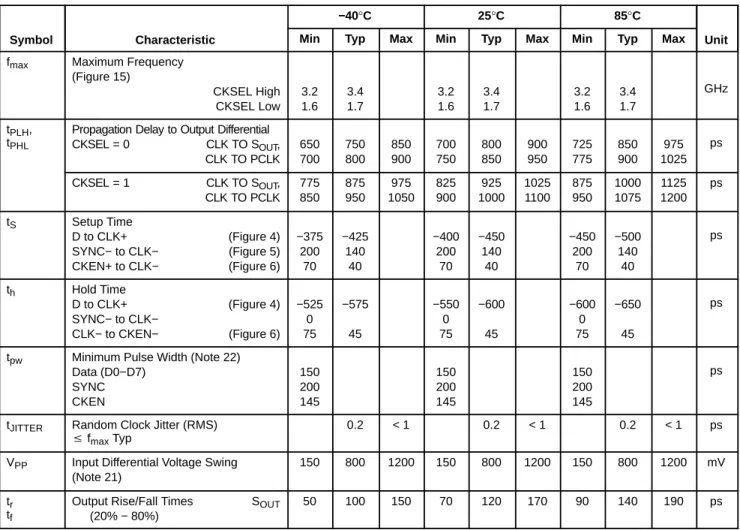
Table 13. AC CHARACTERISTICS VCC = 0 V; VEE = −3.0 V to −5.5 V or VCC = 3.0 V to 5.5 V; VEE = 0 V (Note 20)
Symbol Characteristic
−40°C 25°C 85°C
Unit
Min Typ Max Min Typ Max Min Typ Max
fmax Maximum Frequency (Figure 15) CKSEL High CKSEL Low 3.2 1.6 3.4 1.7 3.2 1.6 3.4 1.7 3.2 1.6 3.4 1.7 GHz
tPLH, tPHL
Propagation Delay to Output Differential CKSEL = 0 CLK TO SOUT,
CLK TO PCLK 650 700 750 800 850 900 700 750 800 850 900 950 725 775 850 900 975 1025 ps
CKSEL = 1 CLK TO SOUT, CLK TO PCLK
775 850 875 950 975 1050 825 900 925 1000 1025 1100 875 950 1000 1075 1125 1200 ps
tS Setup Time
D to CLK+ (Figure 4) SYNC− to CLK− (Figure 5) CKEN+ to CLK− (Figure 6)
−375 200 70 −425 140 40 −400 200 70 −450 140 40 −450 200 70 −500 140 40 ps
th Hold Time
D to CLK+ (Figure 4) SYNC− to CLK−
CLK− to CKEN− (Figure 6) −525 0 75 −575 45 −550 0 75 −600 45 −600 0 75 −650 45 ps
tpw Minimum Pulse Width (Note 22) Data (D0−D7) SYNC CKEN 150 200 145 150 200 145 150 200 145 ps
tJITTER Random Clock Jitter (RMS)
v fmax Typ
0.2 < 1 0.2 < 1 0.2 < 1 ps
VPP Input Differential Voltage Swing (Note 21)
150 800 1200 150 800 1200 150 800 1200 mV
tr tf
Output Rise/Fall Times SOUT (20% − 80%)
50 100 150 70 120 170 90 140 190 ps
NOTE: Device will meet the specifications after thermal equilibrium has been established when mounted in a test socket or printed circuit board with maintained transverse airflow greater than 500 lfpm. Electrical parameters are guaranteed only over the declared operating temperature range. Functional operation of the device exceeding these conditions is not implied. Device specification limit values are applied individually under normal operating conditions and not valid simultaneously.
20. Measured using a 750 mV source, 50% duty cycle clock source. All loading with 50 W to VCC − 2.0 V. 21. VPP(min) is the minimum input swing for which AC parameters are guaranteed.
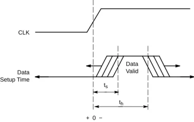
CLK SYNC SYNC
ts
CLK
tS CLK
th CKEN
Figure 4. Setup and Hold Time for Data
th ts Data
Setup Time
+ 0 − CLK
Figure 5. Setup Time for SYNC Figure 6. Setup and Hold Time for CKEN
Data Valid
APPLICATION INFORMATION
The MC10/100EP446 is an integrated 8:1 parallel to serial
converter. An attribute for EP446 is that the parallel inputs
D0–D7 (Pins 17 – 24) can be configured to accept either
CMOS, ECL, or TTL level signals by a combination of
interconnects between V
EF(Pin 27) and V
CF(Pin 26) pins.
For CMOS input levels, leave V
EFand V
CFopen. For ECL
operation, short V
CFand V
EF(Pins 26 and 27). For TTL
operation, connect a 1.5 V supply reference to V
CFand leave
the V
EFpin open. The 1.5 V reference voltage to V
CFpin can
be accomplished by placing a 1.5 k
W
or 500
W
between V
CFand V
EEfor 3.3 V or 5.0 V power supplies, respectively.
Note: all pins requiring ECL voltage inputs must have a
50
W
terminating resistor to V
TT(V
TT= V
CC– 2.0 V).
The CKSEL input (Pin 2) is provided to enable the user to
select the serial data rate output between internal clock data
rate or twice the internal clock data rate. For CKSEL LOW
operation, the time from when the parallel data is latched
¬
to when the data is seen on the S
OUT
is on the falling edge
of the 7
thclock cycle plus internal propagation delay
(Figure 7). Note the PCLK switches on the falling edge of
CLK.
Figure 7. Timing Diagram 1:8 Parallel to Serial Conversion with CKSEL LOW
CLK
SOUT
PCLK
D0 D0−2
D1 D2 D3 D4 D5 D6 D7
D2−2 D3−2 D4−2 D5−2 D6−2 D7−2
D0−3 D1−3 D2−3 D3−3 D4−3 D5−3 D6−3 D7−3 D1−2
CKSEL
D0−1 D1−1 D2−1 D3−1 D4−1 D5−1 D6−1 D7−1 D0−2 D1−2 D2−2 D3−2 D6−2 D0−1
D2−1 D3−1 D4−1 D5−1 D6−1 D7−1 D1−1
D5−2
D0−4 D1−4 D2−4 D3−4 D4−4 D5−4 D6−4 D7−4
1 2 3 4 5 6 7
Number of Clock Cycles from Data Latch to SOUT
Data Latched
Data Latched Data Latched Data Latched
D4−2
À
Similarly, for CKSEL HIGH operation, the time from when the parallel data is latched
¬
to when the data is seen on the
S
OUT
is on the rising edge of the 14
thclock cycle plus internal propagation delay (Figure 8). Furthermore, the PCLK switches
on the rising edge of CLK.
Data Latched Data Latched Data Latched
Figure 8. Timing Diagram 1:8 Parallel to Serial Conversion with CKSEL HIGH
CLK
SOUT
PCLK
D0 D0−1
D1 D2 D3 D4 D5 D6 D7
D2−1 D3−1 D4−1 D5−1 D6−1 D7−1 D1−1
CKSEL
D0−2 D1−2 D2−2 D3−2 D4−2 D5−2 D6−2 D7−2
D0−3 D1−3 D2−3 D3−3 D4−3 D5−3 D6−3 D7−3
D0−1 D1−1 D2−1 D3−1 D4−1 D5−1 D6−1 D7−1 D0−2 D1−2 1 2 3 4 5 6 7 8 9 10 11 12 13 14
À
Á
The device also features a differential SYNC input (Pins 29 and 30), which asynchronously reset all internal flip–flops and
clock circuitry on the rising edge of SYNC. The release of SYNC is a synchronous process, which ensures that no runt serial
data bits are generated. The falling edge of the SYNC followed by a falling edge of CLK initiates the start of the conversion
process on the next rising edge of CLK (Figures 9 and 10). As shown in the figures below, the device will start to latch the
parallel input data after the a falling edge of SYNC
¬
, followed by the falling edge CLK
, on the next rising of edge of CLK
®
for CKSEL LOW
Figure 9. Timing Diagram 1:8 Parallel to Serial Conversion with CKSEL LOW and SYNC
CLK SYNC
SOUT
PCLK
D0 D0−2
D1 D2 D3 D4 D5 D6 D7
D2−2 D3−2 D4−2 D5−2 D6−2 D7−2
D0−3 D1−3 D2−3 D3−3 D4−3 D5−3 D6−3 D7−3 D1−2
CKSEL
D0−1 D1−1 D2−1 D3−1 D4−1 D5−1 D6−1 D7−1 D0−2 D1−2 D2−2 D3−2 D4−2 D6−2 D0−1
D2−1 D3−1 D4−1 D5−1 D6−1 D7−1 D1−1
D5−2
D0−4 D1−4 D2−4 D3−4 D4−4 D5−4 D6−4 D7−4
1 2 3 4 5 6 7
Data Latched
Data Latched Data Latched Data Latched
Figure 10. Synchronous Release of SYNC for CKSEL LOW
CLK SYNC SYNC
(Asynchronous RESET)
À
Á
Â
À
Á
Â
SYNC (Synchronous ENABLE)
For CKSEL HIGH, as shown in the timing diagrams below, the device will start to latch the parallel input data after the falling
edge of SYNC
¬
, followed by the falling edge CLK
, on the second rising edge of CLK
®
(Figures 11 and 12).
Figure 11. Timing Diagram 1:8 Parallel to Serial Conversion with CKSEL HIGH and SYNC
CLK SYNC
SOUT
PCLK
D0 D0−1
D1 D2 D3 D4 D5 D6 D7
D2−1 D3−1 D4−1 D5−1 D6−1 D7−1 D1−1
CKSEL
D0−2 D1−2 D2−2 D3−2 D4−2 D5−2 D6−2 D7−2
D0−3 D1−3 D2−3 D3−3 D4−3 D5−3 D6−3 D7−3
D0−4 D1−4 D2−4 D3−4 D4−4 D5−4 D6−4 D7−4
D0−1 D1−1 D2−1 D3−1 D4−1 D5−1 D6−1 D7−1 D0−2 D1−2 1 2 3 4 5 6 7
Data Latched
8 9 10 11 12 13 14
Data Latched Data Latched
Figure 12. Synchronous Release of SYNC for CKSEL HIGH
CLK SYNC
À
Á Â
SYNC (Asynchronous RESET)
SYNC (Synchronous ENABLE)
À
Á Â
The differential synchronous CKEN inputs (Pins 6 and 7), disable the internal clock circuitry. The synchronous CKEN will
suspend all of the device activities and prevent runt pulses from being generated. The rising edge of CKEN followed by the
falling edge of CLK will suspend all activities. The falling edge of CKEN followed by the falling edge of CLK will resume
all activities (Figure 13).
Figure 13. Timing Diagram with CKEN with CKSEL HIGH
CLK
CKEN SOUT
CKSEL
D1−1
D0−1 D2−1 D3−1
PCLK
D4−1 D5−1 Internal Clock
Disabled Internal ClockEnabled
The differential PCLK output (Pins 14 and 15) is a word
framer and can help the user synchronize the serial data
output, S
OUT(Pins 11 and 12), in their applications.
Furthermore, PCLK can be used as a trigger for input
parallel data (Figure 14).
An internally generated voltage supply, the V
BBpin, is
available to this device only. For single–ended input
conditions, the unused differential input is connected to V
BBas a switching reference voltage. V
BBmay also rebias AC
coupled inputs. When used, decouple V
BBand V
CCvia a
0.01
m
F capacitor and limit current sourcing or sinking to
0.5 mA. When not used, V
BBshould be left open. Also, both
outputs of the differential pair must be terminated (50
W
to
V
TT) even if only one output is used.
Figure 14. PCLK as Trigger Application
TRIGGER
Pattern Generator Data Format Logic
(FPGA, ASIC)
P
ARALLEL
DA
T
A
OUTPUT
CLK
PCLK
EP446
P
ARALLEL
DA
T
A
INPUT
SYNC
SOUT SERIAL DATA CLK RESET
0 100 200 300 400 500 600 700 800
0 500 1000 1500 2000 2500 3000 3500
Figure 15. Typical VOUTPP versus Input Clock Frequency, 255C
INPUT CLOCK FREQUENCY (MHz) VOUTpp
(mV)
CKSEL Low
CKSEL High
Figure 16. SOUT System Jitter Measurement
Figure 17. Typical Termination for Output Driver and Device Evaluation (See Application Note AND8020/D − Termination of ECL Logic Devices.)
Driver Device
Receiver Device
Q D
Q D
Zo = 50 W
Zo = 50 W
50 W 50 W
VTT VTT = VCC − 2.0 V
ORDERING INFORMATION
Device Package Shipping†
MC10EP446FAG LQFP−32
(Pb−Free)
250 Units / Tray
MC10EP446FAR2G 2000 / Tape & Reel
MC10EP446MNG QFN−32
(Pb−Free)
74 Units / Rail
MC100EP446MNG 74 Units / Rail
MC100EP446FAG LQFP−32
(Pb−Free)
250 Units / Tray
MC100EP446FAR2G 2000 / Tape & Reel
MC10EP446MNR4G QFN−32
(Pb−Free)
1000 / Tape & Reel
MC100EP446MNR4G 1000 / Tape & Reel
†For information on tape and reel specifications, including part orientation and tape sizes, please refer to our Tape and Reel Packaging Specifications Brochure, BRD8011/D.
Resource Reference of Application Notes AN1405/D − ECL Clock Distribution Techniques
AN1406/D − Designing with PECL (ECL at +5.0 V)
AN1503/D − ECLinPSt I/O SPiCE Modeling Kit
AN1504/D − Metastability and the ECLinPS Family
AN1568/D − Interfacing Between LVDS and ECL
AN1672/D − The ECL Translator Guide
AND8001/D − Odd Number Counters Design
AND8002/D − Marking and Date Codes
AND8020/D − Termination of ECL Logic Devices
AND8066/D − Interfacing with ECLinPS
PACKAGE DIMENSIONS
ÉÉ ÉÉ ÉÉ DETAIL Y A S1 V B 1 8 9 17 25 32 AE AE PDETAIL Y BASE
N J D F METAL SECTION AE−AE G SEATING PLANE R Q_ W K X 0.250 (0.010) GAUGE PLANE E C H DETAIL AD DETAIL AD A1 B1 V1 4X S 4X 9 −T− −Z− −U− T-U 0.20 (0.008) AC Z
T-U 0.20 (0.008) AB Z
0.10 (0.004) AC
−AC− −AB−
M_
8X
−T−, −U−, −Z−
T-U
M
0.20 (0.008)
Z
AC
32 LEAD LQFP
CASE 873A−02 ISSUE C
NOTES:
1. DIMENSIONING AND TOLERANCING PER ANSI Y14.5M, 1982.
2. CONTROLLING DIMENSION: MILLIMETER.
3. DATUM PLANE −AB− IS LOCATED AT BOTTOM OF LEAD AND IS COINCIDENT WITH THE LEAD WHERE THE LEAD EXITS THE PLASTIC BODY AT THE BOTTOM OF THE PARTING LINE. 4. DATUMS −T−, −U−, AND −Z− TO BE
DETERMINED AT DATUM PLANE −AB−. 5. DIMENSIONS S AND V TO BE
DETERMINED AT SEATING PLANE −AC−. 6. DIMENSIONS A AND B DO NOT
INCLUDE MOLD PROTRUSION. ALLOWABLE PROTRUSION IS 0.250 (0.010) PER SIDE. DIMENSIONS A AND B DO INCLUDE MOLD MISMATCH AND ARE DETERMINED AT DATUM PLANE −AB−.
7. DIMENSION D DOES NOT INCLUDE DAMBAR PROTRUSION. DAMBAR PROTRUSION SHALL NOT CAUSE THE D DIMENSION TO EXCEED 0.520 (0.020). 8. MINIMUM SOLDER PLATE THICKNESS
SHALL BE 0.0076 (0.0003). 9. EXACT SHAPE OF EACH CORNER
MAY VARY FROM DEPICTION.
DIM A
MIN MAX MIN MAX INCHES 7.000 BSC 0.276 BSC MILLIMETERS
B 7.000 BSC 0.276 BSC C 1.400 1.600 0.055 0.063 D 0.300 0.450 0.012 0.018 E 1.350 1.450 0.053 0.057 F 0.300 0.400 0.012 0.016 G 0.800 BSC 0.031 BSC H 0.050 0.150 0.002 0.006 J 0.090 0.200 0.004 0.008 K 0.450 0.750 0.018 0.030 M 12 REF 12 REF N 0.090 0.160 0.004 0.006 P 0.400 BSC 0.016 BSC Q 1 5 1 5 R 0.150 0.250 0.006 0.010
V 9.000 BSC 0.354 BSC V1 4.500 BSC 0.177 BSC
_ _
_ _ _ _
B1 3.500 BSC 0.138 BSC A1 3.500 BSC 0.138 BSC
S 9.000 BSC 0.354 BSC S1 4.500 BSC 0.177 BSC
W 0.200 REF 0.008 REF X 1.000 REF 0.039 REF
PACKAGE DIMENSIONS
QFN32 5x5, 0.5P
CASE 488AM ISSUE A SEATING NOTE 4 K 0.15 C (A3) A A1 D2 b 1 9 17 32 E2 32X 8 L 32X BOTTOM VIEW TOP VIEW SIDE VIEW D A B E 0.15 C É É PIN ONE LOCATION 0.10 C 0.08 C C 25 e NOTES:
1. DIMENSIONS AND TOLERANCING PER ASME Y14.5M, 1994.
2. CONTROLLING DIMENSION: MILLIMETERS. 3. DIMENSION b APPLIES TO PLATED
TERMINAL AND IS MEASURED BETWEEN 0.15 AND 0.30MM FROM THE TERMINAL TIP. 4. COPLANARITY APPLIES TO THE EXPOSED
PAD AS WELL AS THE TERMINALS.
PLANE
*For additional information on our Pb−Free strategy and soldering details, please download the ON Semiconductor Soldering and Mounting Techniques Reference Manual, SOLDERRM/D.
SOLDERING FOOTPRINT* 0.50 3.35 0.30 3.35 32X 0.63 32X 5.30 5.30 L1 DETAIL A L ALTERNATE TERMINAL CONSTRUCTIONS L ÉÉÉ ÇÇÇ ÇÇÇ DETAIL B MOLD CMPD EXPOSED Cu ALTERNATE CONSTRUCTION DETAIL B DETAIL A DIM A MIN MILLIMETERS 0.80 A1 −−−
A3 0.20 REF
b 0.18
D 5.00 BSC
D2 2.95
E 5.00 BSC 2.95
E2
e 0.50 BSC 0.30 L K 0.20 1.00 0.05 0.30 3.25 3.25 0.50 −−− MAX −−− L1 0.15 e/2 NOTE 3 PITCH DIMENSION: MILLIMETERS RECOMMENDED A M
0.10 C B
M
0.05 C
ON Semiconductor and are registered trademarks of Semiconductor Components Industries, LLC (SCILLC). SCILLC owns the rights to a number of patents, trademarks,
copyrights, trade secrets, and other intellectual property. A listing of SCILLC’s product/patent coverage may be accessed at www.onsemi.com/site/pdf/Patent−Marking.pdf. SCILLC reserves the right to make changes without further notice to any products herein. SCILLC makes no warranty, representation or guarantee regarding the suitability of its products for any particular purpose, nor does SCILLC assume any liability arising out of the application or use of any product or circuit, and specifically disclaims any and all liability, including without limitation special, consequential or incidental damages. “Typical” parameters which may be provided in SCILLC data sheets and/or specifications can and do vary in different applications and actual performance may vary over time. All operating parameters, including “Typicals” must be validated for each customer application by customer’s technical experts. SCILLC does not convey any license under its patent rights nor the rights of others. SCILLC products are not designed, intended, or authorized for use as components in systems intended for surgical implant into the body, or other applications intended to support or sustain life, or for any other application in which the failure of the SCILLC product could create a situation where personal injury or death may occur. Should Buyer purchase or use SCILLC products for any such unintended or unauthorized application, Buyer shall indemnify and hold SCILLC and its officers, employees, subsidiaries, affiliates, and distributors harmless against all claims, costs, damages, and expenses, and reasonable attorney fees arising out of, directly or indirectly, any claim of personal injury or death associated with such unintended or unauthorized use, even if such claim alleges that SCILLC was negligent regarding the design or manufacture of the part. SCILLC is an Equal Opportunity/Affirmative Action Employer. This literature is subject to all applicable copyright laws and is not for resale in any manner.
PUBLICATION ORDERING INFORMATION
N. American Technical Support: 800−282−9855 Toll Free
USA/Canada
Europe, Middle East and Africa Technical Support:
Phone: 421 33 790 2910
ECLinPS is a trademark of Semiconductor Components Industries, LLC (SCILLC)
LITERATURE FULFILLMENT:
Literature Distribution Center for ON Semiconductor P.O. Box 5163, Denver, Colorado 80217 USA
Phone: 303−675−2175 or 800−344−3860 Toll Free USA/Canada
ON Semiconductor Website: www.onsemi.com Order Literature: http://www.onsemi.com/orderlit