AENSI Journals
Australian Journal of Basic and Applied Sciences
ISSN:1991-8178Journal home page: www.ajbasweb.com
Corresponding Author: Koh Wen Shi, Freescale Semiconductor (M) Sdn. Bhd., Free Industrial Zone Sungei Way, 47300 Petaling Jaya, Selangor, Malaysia.
E-mail: [email protected]
Optimization of Wafer Singulation Process on Copper/Low-k Materials for
Semiconductor Device Assembly
1,3Koh Wen Shi, 2Yap Boon Kar, 1Halina Misran, 3Yow Kai Yun, 3Lo Wei Yew and 3Tan Cai Hui
1Department of Mechanical Engineering, College of Engineering, Universiti Tenaga Nasional, KM-7, Jalan Ikram-Uniten, 43009 Kajang, Selangor, Malaysia.
2Center of Microelectronic and Nanotechnology Engineering (CeMNE), College of Engineering, Universiti Tenaga Nasional, Jalan Ikram- Uniten, 43009 Kajang, Selangor, Malaysia.
3Freescale Semiconductor (M) Sdn. Bhd., Free Industrial Zone Sungei Way, 47300 Petaling Jaya, Selangor, Malaysia.
A R T I C L E I N F O A B S T R A C T
Article history:
Received 15 September 2014 Accepted 5 October 2014 Available online 25 October 2014
Keywords:
Cutting, Dicing, Singulation, Copper, Low-k dielectrics, Silicon wafer, Diamond blade
This paper presents a wafer singulation process optimization by using a Cu/Low-k metallized wafer as part of the effort to enhance the processing yield and quality. Reported are results from a Design of Experiment (DOE) to look into the effects of the blade type, the blade rotation speed, and the cutting depth on improving the dicing quality. Optical visual inspection was performed on the post-processed Cu/Low-k metallized wafer, specifically along the scribe structures comprised of high metal density in order to assess the level of the die chipping, cracking and peeling quality. Electrical testing and reliability stressing assessments were followed to validate the newly established dicing parameter is robust. It is shown that, with an appropriate dicing saw blade and an optimum dicing parameter applied, the produced cutting quality of production environment has improved significantly.
© 2014 AENSI Publisher All rights reserved. To Cite This Article: Koh Wen Shi, Yap Boon Kar, Halina Misran, Yow Kai Yun, Lo Wei Yew and Tan Cai Hui., Design Requirements Clarification for Body Area Network: Application to In-Patients. Aust. J. Basic & Appl. Sci., 8(22):6-11, 2014
INTRODUCTION
Blade dicing is the most common dicing techniques used in the semiconductor industry. In recent years in the continuous improvement and advancement of Copper (Cu)/low-k wafer technology, which involving the inter-layer dielectric (ILD) materials changes from traditional silicon dioxide (SiO2) ILD to a much weaker property in mechanical and adhesion strength of Cu/low-k ILD. This change was pushed by many semiconductor industry participants as there are demands and needs to get low cost, high functioning, fast speed, high reliability and low interconnect delay package in the future (Z.J. Wang, 2005; M. Brillouet, 2006; W.S. Koh, 2010). Every bit the chip size continuous to shrink down with the applications of Cu/low-k materials technology, it will bring challenges to the semiconductor device packaging and fabrication procedures, especially for blade sawing process (H. Zhao, 2003; W.D. Driel, 2007). Cu/low-k wafer dicing using a diamond blade has high potential results poor topside cutting quality. There are issues encountered when dicing through the wafer comprised of thicker ILD stack and higher metal density; namely ILD peeling/delamination, die chipping, and cracking. Those are the most common dicing defects found and not acceptable due to the drastic impacts of the assembly yield loss and package reliability (A.T. Cheung, 2005; W.S. Koh, 2013).
Research Methodology and Experimentation: I. Experimental Wafer Information:
The selected test vehicle in this project is a pizza mask wafer which consists of multiple device designs on a single wafer. There is a total of 3 different die devices in each wafer, which needs to be singulated for ILD peeling and die chipping assessments. The test vehicle was designed and fabricated with a 55nm Cu/low-k wafer process technology. The wafer surface was electroplated with a 3um thick metallization on top of the aluminium (Al) bonding pads and test patterns on the saw street. The metal compounds on the thick metallization contain a combination of nickel, gold and palladium elements. Dicing through the thick metal composite tends to result more ILD peeling and chipping defects due to the hard and brittle structures in nature. The following dicing assessments were conducted to develop a robust saw process capability on dicing through the complicated Cu metals, low-k dielectric films and thick electroplating metallization.
II. Dicing Blade Selection and Dicing Process Variables Optimization:
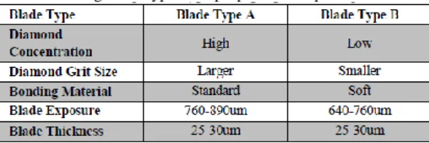
Choosing a suitable dicing blade is very important. The key factors that one needs to take when choosing a new blade are diamond grit size, diamond grit concentration and bonding material. 2 types of dicing blades were evaluated in this experiment. A comparison of the 2 dicing blade properties is presented in Table 1.
Table 1: Dicing blade types and properties comparison.
The hypothesis, based on practical experiences and theory, shown that lower table speed, higher Z1 rotation and lower Z1 cut depth are likely and in favour to produce good cutting quality. Higher Z1 rotation helps to bring down the topside peeling and delamination because the entire workload and stresses affected on Z1 blade is lower during cutting; blade wobbling and vibration are less/little. Higher table speed is favourable for higher throughput and productivity, however, it will result in high work load and stresses in the blade, result higher blade vibration and wobbling, and the blade stability during cutting is easily get affected, expected to observe more worse case ILD peeling and die chipping after sawing. Shallow or lower Z1 cut depth can result better topside peeling and chipping. Unfortunately, the all mentioned process variables above and its effects on the overall cutting quality are greatly depend on the type of the materials used in their wafer technology and fabrication process, specifically for the thicker and higher ILD stack structures will be harder to singulate and may have imposed dicing difficulty due to the metal content and density across the saw street are significantly different from Cu/low-k wafer compared to the traditional non Cu/low-k wafer (W.S. Koh, 2009).
Improper dicing blade selections as well as using a not optimized dicing process parameters have higher probabilities of producing undesirable die topside cutting quality. Dicing quality with existing control parameters was not satisfactory and dicing process parameter optimization have had planned and contrived to better cutting quality on unfriendly Al scribe structures. The topside of Al scribe structures has additional 3um of thick electroplating metallization. In order to establish a new dicing recipe capable of processing a 55nm Cu/low-k wafer, a 3-factor full factorial DOE model was conducted in order to optimize the topside ILD peeling and chipping performance, see Table 2. The DOE model consists of 3 variables, blade type (A vs. B), Z1 blade rotation speed and Z1 cut depth into Si. A total of 10 DOE wafers are required to complete the 8 run orders plus 2 center point parameters in this experiment. Step cut mode cutting is applied, whereby the Z1 blade is cut into the topside of wafer surface while the Z2 blade will be followed to cut all the way through the backside of the wafer, Z2 blade has to cut into the dicing tape for about ~33% of the total dicing tape thickness to ensure the die is completely singulated.
RESULTS AND DISCUSSION
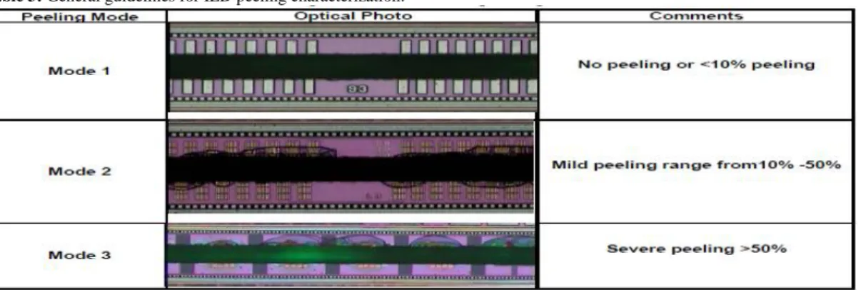
A total of 10 runs was conducted and the input process factors included in this experiment are dicing blade types, Z1 blade spindle rotations and Z1 blade cutting depth into Si. This is part of our endeavour to specify the best optimized saw process parameter for Cu/low-k, hard, brittle and heavy metallization (via electroplating) wafer. Die corner peeling, die side ILD peeling and die topside chipping visual inspection were performed thoroughly after blade sawing. The sample size was selected randomly, 5 full reticle per wafer per run order inspected, focused on die with sensitive scribe structures which will have a higher tendency to cause ILD peeling and delamination. Table 3 shows the inspection criteria to follow and illustrate how to categorize the mode-1, -2, and -3 peeling that observed at the particular scribe feature during visual inspection. There is a checklist for the inspector to fill out how many mode-1, -2 and -3 peeling observed for all run orders. Every run order in this experiment will consists of mode-1, -2 and -3 peeling by the number of counts or frequencies. Grading will be put to every peeling mode observed so that the overall dicing quality and operation can be evaluated, interpreted and demonstrated by a final score. The maximum final score obtained from a run order indicate good cutting quality. The minimum final score obtained from a run order indicate bad cutting quality.
Table 3: General guidelines for ILD peeling characterization.
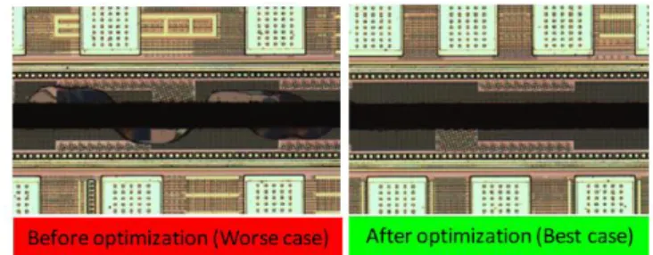
The distribution of ILD peeling and die chipping across all the run order is shown in Fig. 1. According to the bar chart in Fig. 1, RO4 turns out to be the best run in this DOE for ILD peeling and die chipping performance. The worst cell for ILD peeling and die chipping performance is RO3 (faster Z1 blade rotation speed, deeper Z1 cut depth into Si and using blade type B). Thus, lower Z1 blade rotation speed, deeper Z1 cut depth into Si and using blade type A are more favourable for better topside chipping and peeling performance. Optical photo of the die topside ILD peeling is shown in Fig. 2, compare before and after dicing process optimization. Unlike for faster Z1 blade rotation speed, adverse effects resulted along the cutting edge with high peeling and chipping. Mode 3 ILD peeling and delamination are not possible to be completely eliminated for the best optimized dicing recipe in this experiment. However, the mode 3 ILD peeling can be well controllable outside the die edge seal ring, and peeling breach over the die edge seal ring must not accept.
Fig. 2: Best case versus worst case dicing quality comparing before and after dicing process optimization.
Focused ion beam (FIB) cross sectional analysis was performed in the worst case mode 3 peeling to inspect the depth of the ILD peeling, result indicates that the ILD peeling was occurred only at the surface level and does not affect the underneath metallization. Fig. 3 shows the optical photo with the FIB cross sectional done at the peeling area shown in red.
Fig. 3: Optical and scanning electron microscope (SEM) micrograph reveal no delamination further into die active layer, the ILD peeling was occurring only at the surface level and does not affect the underneath metallization.
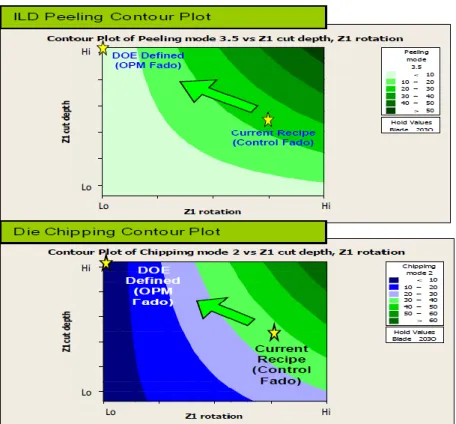
In order to reduce the ILD peeling and die chipping size, the overall response optimizer suggests to use the blade type C, the lower Z1 blade rotation and the deeper Z1 cutting depth into Si, see Fig. 4. The desirability for this prediction profile is fairly reliable and good, which reads at about 95%.
Fig. 4: ILD peeling and die chipping responses optimizer.
Fig 5: Contour plots for ILD peeling and die chipping.
Therefore, the suggested best dicing recipe in this experiment is RO4, based on the statistical results as well as the validation and confirmation done by using optical visual inspection and SEM examination. Lower Z1 blade rotation speed is much more favourable for better ILD peeling and chipping performance for Cu/low-k wafers. Observed mode 3 peeling for the best cell only occurred at surface level and is not extended into the active die layers. Package reliability and stressing were performed as part of the exercise to validate the established dicing recipe is robust and workable on Cu/low-k wafer. The assembled IC packages have passed MSL level 3 at 260C preconditioning; underwent confocal scanning acoustic microscopy (CSAM) examination result looks good, electrical testing was also conducted at the following temperature cycle in 500, 1000 and 1500 read point confirmed no failure found related to the blade dicing process.
Future Work and Recommendations:
Based on all the experimental studies that were performed, the results show that blade dicing process alone is not possible to produce zero dicing defects. Dicing through the unfriendly scribe patterns with a higher metal density still exhibits metal layer delamination, ILD peeling and die chipping. Hence forth, on future works and recommendations, laser grooving could be seen as another option in order to get a true dicing defect-free process (T.A., Tran, 2012).
Unlike traditional blade dicing, laser grooving is a thermal energy based process; with no direct tool-to-work piece contact. When a focused laser beam with high energy density contacts the Si wafer, thermal energy is transferred and absorbed by Si; heat will transform to the Cu/low-k ILD metal layers and melted into molten and the solids are vaporized, which can be disposed and removed by the flow of air pressure. This new advanced dicing process technology can be an opportunity to resolve the dicing challenges with more upcoming Cu/low-k and ULK wafers (K.S. Lee, 2006; T.B. Lau, 2008; W.S. Koh, 2009; K.Y. Yow, 2010).
Conclusions:
ACKNOWLEDGEMENT
The authors would like to thank LC Tan, and TSO-PAE engineers from Freescale Semiconductor (M) Sdn. Bhd., for providing technical assistance, guidance and supports. This project is funded by the Ministry of Higher Education (Grant Number: 2014109FRGS).
REFERENCES
Brillouet, M., 2006. Challenges in Advanced Metallization Schemes, Microelectronic Engineering, (83): 2036-2041.
Cheung, T.A., 2005. Dicing Advanced Materials for Microelectronics, IEEE International Symposium on Advanced Packaging Materials: Processes, Properties and Interfaces, page 149-152.
Driel, W.D., 2007. Facing the Challenge of Designing for Cu/Low-k Reliability, Microelectronics Reliability, 47: 1969-1974.
Jacob, P., W. Rothkirch, 2008. Unusual Defects, Generated by Wafer Sawing: Diagnosis, Mechanisms and How to Distinguish from Related Failures, Microelectronics Reliability, 48: 1253-1257.
Koh, W.S., K.Y. Yow, L.H. Khoo, W.Y. Lo, 2009. Wafer Dicing Process Optimization and Characterization for C90 Low-k Wafer Technology, IEEE International Conference on Electronic Packaging Technology, page 889-892.
Koh, W.S., T.B. Lau, K.Y. Yow, 2009. Laser Grooving Characterization for Dicing Defects Reduction and its Challenges, IEEE International Conference on Electronic Packaging Technology, page 846-850.
Koh, W.S., 2010. Developments of Blade Dressing Technique using SiC Board for C90 Low-k Wafer Sawing, IEEE International Conference on Electronic Packaging Technology, page 122-128.
Koh, W.S., K.Y. Yow, 2013. The Characteristics and Factors of a Wafer Dicing Blade and its Optimized Interactions Required for Singulating High Metal Stack Low-k Wafers, IEEE International Conference on Electronic Packaging Technology, page 208-212.
Lau, T.B., Y.W. Lo, W.S. Koh, C.T. Siong, K.Y. Yow, 2008. Laser Grooving Process Development for Low-k / Ultra Low-k Devices, IEEE International Conference on Electronic Manufacturing Technology, page 1-6.
Lee, K.S., 2006. Laser as a Future Direction for Wafer Dicing: Parametric Study and Quality Assessment,
IEEE International Conference on Electronic Manufacturing Technology, page 506-509.
Tran, T.A., V. Mathew, W.S. Koh, K.Y. Yow, Y.K. Au, 2012. Overcoming Dicing Challenges for Low-K Copper Wafers using Nickel-Palladium-Gold Bond Pads for Automotive Application, IEEE International Conference on Electronic Manufacturing Technology, page 364-371.
Wang, Z.J., S. Wang, J.H. Wang, S. Lee, S.Y. Yao, R. Han, Y.Q. Su, 2005. 300mm Low-k Wafer Dicing Saw Study, IEEE International Conference on Electronic Packaging Technology, page 262-268.
Yow, K.Y., W.S. Koh, 2010. Laser Grooving on Narrow Scribe Widths on Thick Flip Chip Wafer: The Challenges and its Resolution, IEEE International Conference on Electronic Packaging Technology, page 369-372.