Application Report
SLLA083A - SEPTEMBER 2000
1
Low-Voltage, Single-Supply
232-Standard Interface Solutions
Jose M. Soltero, Jing Zhang, and Ernest Cox Linear Products
ABSTRACT
Features and key specifications for Texas Instruments (TI) new low-voltage, single-supply, 232-standard-compliant interface devices are presented, as well as test data comparing TI versus competitor same-function devices. Evolution of the 232 standard is discussed relative to TI devices that have significantly greater capability than the 232 standard requires.
Contents
Introduction . . . 3
Brief Overview of the 232 Standard . . . 3
ANSI TIA/EIA-232-F Electrical Specification . . . 4
232-Standard Handshaking Signals for DB9S Connections . . . 5
Technology Evolution . . . 6
Key Features and Related Benefits . . . 7
Typical Design Applications . . . 8
Analysis of TI and Competitor Equivalent Devices . . . 11
Driver Output Voltage. . . 11
Supply Current . . . 12
Slew Rate. . . 14
Conclusion . . . 17
Reference . . . 17
List of Figures 1 Changes in 232-Standard Transition Times vs Data Rates . . . 4
2 Driver and Receiver Voltage Levels . . . 5
3 Typical Host (DTE) and Peripheral (DCE) System Application. . . 9
4 Null Modem Wiring Diagram. . . 10
5 Competing Device Output Voltage vs CL (VCC = 3.3 V) . . . 11
6 Competing Device Output Voltage vs CL (VCC = 5 V) . . . 11
7 TI Device Output Voltage vs CL (VCC = 3.3 V) . . . 12
8 TI Device Output Voltage vs CL (VCC = 5 V) . . . 12
9 Competing Device Supply Current vs CL (VCC = 3.3 V) . . . 12
10 Competing Device Supply Current vs CL (VCC = 5 V) . . . 13
11 TI Device Supply Current vs CL (VCC = 3.3 V) . . . 13 TI is a trademark of Texas Instruments.
12 TI Device Supply Current vs CL (VCC = 5 V). . . 13
13 Competing Device Slew Rate vs CL (VCC = 3.3 V) . . . 14
14 Competing Device Slew Rate vs CL (VCC = 5 V) . . . 14
15 TI Device Slew Rate vs CL (VCC = 3.3 V) . . . 14
16 TI Device Slew Rate vs CL (VCC = 5 V) . . . 15
17 Competing Device Slew Rate vs Data Rate (VCC = 3.3 V). . . 15
18 Competing Device Slew Rate vs Data Rate (VCC = 5 V) . . . 15
19 TI Device Slew Rate vs Data Rate (VCC = 3.3 V). . . 16
20 TI Device Slew Rate vs Data Rate (VCC = 5 V) . . . 16
List of Tables 1 Key 232-Standard Electrical Specifications . . . 5
2 232 Signal Descriptions . . . 6
3 Device Features and Benefits . . . 7
4 Summary Comparison of TI MAX3243 and Competitor’s ’3243. . . 17
SLLA083A
3 Low-Voltage, Single-Supply 232-Standard Interface Solutions
Introduction
This application report provides information about the new low-voltage, single-supply interface devices produced by TI. These devices include the popular three-driver/five-receiver data terminal equipment (DTE) device named MAX3243, and specifically are designed for the personal computer (PC) serial port I/O, which usually is used with the 9-pin DB9S connector. Another new device is the five-driver/three-receiver data-circuit-terminating equipment (DCE) device named MAX3238, which is the complement to the DTE device, and is commonly used on the peripheral end of the connecting cable. Also, the MAX3221, which is the smallest possible 232-standard solution, with one driver and one receiver per package, is another member of this family of devices.
Until now, TI has not offered pure CMOS 232-interface devices that operate at supply voltages from 3 V to 5.5 V. These three new TI integrated circuits (ICs) incorporate an on-board charge pump that, with four small external capacitors, produces the necessary driver output voltage swings to comply with the 232 standard. Low-power, high human-body model (HBM)
electrostatic discharge (ESD) serial-port protection, high data rates, and small packages are some of the benefits featured on these devices.
Brief Overview of the 232 Standard
Officially, the 232 standard’s title is Interface Between Data Terminal Equipment and Data
Circuit-Terminating Equipment Employing Serial Binary Data Interchange. The current revision is TIA/EIA-232-F (previously referred to as RS-232). In the past, the term RS-232 has been used interchangeably with its official name; however, the RS prefix no longer is used and this
document follows the new terminology. The standard discusses electrical specifications, i.e., the physical layer, protocol requirements, and specifies a 25-pin D-type connector that attaches to the cable. Discussion of mechanical characteristics is beyond the scope of this application report. Protocol is discussed briefly only for signals used with the 9-pin connector.
The 232 standard was introduced in 1962 as an effort to standardize the interface for serial communication between the DTE and DCE. Early adopters emphasized the interface between the PC (DTE) and the modem (DCE). Wide acceptance of the PC quickly ensured that the 232 standard would become the industry standard it is today – a low-cost, serial interface. The mouse, plotter, printer, scanner, digitizer, external modems, and test equipment are examples of peripherals that connect to the 232-compliant serial port.
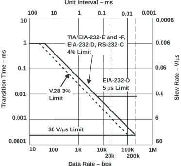
Throughout the years, the 232 standard has been revised a number of times. Figure 1 shows several transition-time vs data-rate changes made to the standard. The latest revision makes 232 specifications agree with international standards ITU-T V.24, V.28, and ISO/IEC 2110.
10
10 100100 1k1k 10k10k 100k100k 1M1M 10
10 10
10 100
100 11
1 1
0.1 0.1
0.1 0.1
0.01 0.01
0.01 0.01 0.0010.001
0.001 0.001
0.0001 0.0001
0.0006 0.0006
0.006 0.006
0.06 0.06
0.6 0.6
6 6
60 60
T
ransition
T
ime – ms
Unit Interval – ms
Slew Rate – V/ s
Data Rate – bps TIA/EIA-232-E and -F, EIA-232-D, RS-232-C 4% Limit
EIA-232-D 5 µs Limit V.28 3%
Limit
30 V/ms Limit
µ
20k 200k
Figure 1. Changes in 232-Standard Transition Times vs Data Rates
TIA/EIA-232-F places four constraints that limit the unit interval, which is the inverse of data rate, and transition time, defined by the slew rate. Referring to Figure 1, the first constraint is set by the top line. The standard specifies that for any data rate less than or equal to 40 bps, the transition time cannot exceed 1 ms. The second constraint is illustrated as the 4%-limit line drawn diagonally from 40 bps to 200 kbps. This specifically states that for any unit interval less than or equal to 25 ms (equivalent to ≥40 bps data rate) but greater than or equal to 50 ms (equivalent to ≤20 kbps data rate), the transition time must not exceed 4% of the unit interval. The third constraint shown pertains to the bottom line, which places a maximum limit of 30 V/ms on the driver output slew rate. This maximum slew rate translates to a minimum transition time of 0.2 ms because 232 voltage swings should never fall below 6 V (0.2 ms = 6 V/30 V/ms). Finally, the fourth limit is data rate, which is widely known in the industry to be only 20 kbps. Hence, the dashed line in Figure 1.
ANSI TIA/EIA-232-F Electrical Specification
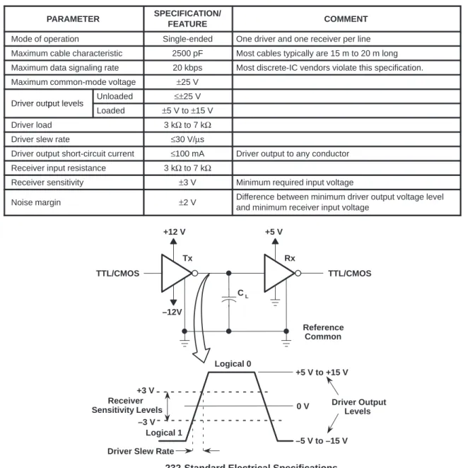
It is evident from the specifications in Table 1 that the 232 standard was created when power considerations were not scrutinized closely and data signaling rates, although adequate at that time, were extremely slow when compared to today’s standards. To be compatible with the original standard, receiver inputs and driver outputs must tolerate ±25-V voltage swings. Continually increasing demand for speed has forced discrete-IC manufacturers to violate the 232-standard maximum 20-kbps specification at the expense of ignoring the 4% limit shown in Figure 1. Today, 250-kbps data-signaling rates are common. Table 1 presents key 232-compliant specifications and features. Figure 2 graphically shows driver and receiver compatibility
SLLA083A
5 Low-Voltage, Single-Supply 232-Standard Interface Solutions Table 1. Key 232-Standard Electrical Specifications
PARAMETER SPECIFICATION/
FEATURE COMMENT
Mode of operation Single-ended One driver and one receiver per line Maximum cable characteristic 2500 pF Most cables typically are 15 m to 20 m long Maximum data signaling rate 20 kbps Most discrete-IC vendors violate this specification. Maximum common-mode voltage ±25 V
Driver output levels Unloaded ≤±25 V Driver output levels
Loaded ±5 V to ±15 V Driver load 3 kΩ to 7 kΩ Driver slew rate ≤30 V/µs
Driver output short-circuit current ≤100 mA Driver output to any conductor Receiver input resistance 3 kΩ to 7 kΩ
Receiver sensitivity ±3 V Minimum required input voltage
Noise margin ±2 V Difference between minimum driver output voltage level and minimum receiver input voltage
TTL/CMOS TTL/CMOS
+12 V
–12V
Reference Common CL
Tx
+5 V
–5 V to –15 V +5 V to +15 V
0 V
Logical 1
Logical 0
+3 V
–3 V
232-Standard Electrical Specifications
Receiver
Sensitivity Levels Driver OutputLevels
Driver Slew Rate
Rx
Figure 2. Driver and Receiver Voltage Levels
232-Standard Handshaking Signals for DB9S Connections
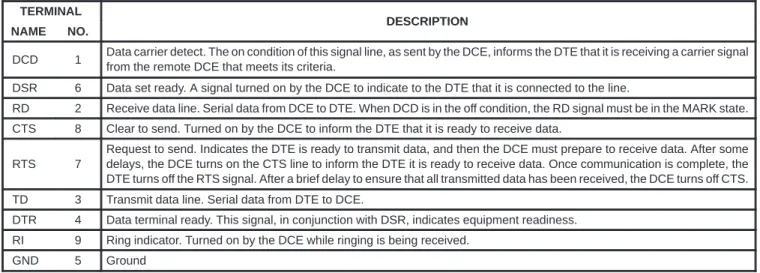
As mentioned previously, the 25-pin connector is recommended in the 232 standard. However, in today’s applications, the 9-pin D-type connector, commonly known as the DB9S connector, is chosen by most users because not all handshaking signals are necessary in most applications. Typically, the handshaking signals used with the DB9S connector are sufficient to support error-free data transmission. A description of the protocol signals and their corresponding DB9S connector pins are presented in Table 2.
Table 2. 232 Signal Descriptions
TERMINAL
DESCRIPTION
NAME NO. DESCRIPTION
DCD 1 Data carrier detect. The on condition of this signal line, as sent by the DCE, informs the DTE that it is receiving a carrier signal from the remote DCE that meets its criteria.
DSR 6 Data set ready. A signal turned on by the DCE to indicate to the DTE that it is connected to the line.
RD 2 Receive data line. Serial data from DCE to DTE. When DCD is in the off condition, the RD signal must be in the MARK state. CTS 8 Clear to send. Turned on by the DCE to inform the DTE that it is ready to receive data.
RTS 7
Request to send. Indicates the DTE is ready to transmit data, and then the DCE must prepare to receive data. After some delays, the DCE turns on the CTS line to inform the DTE it is ready to receive data. Once communication is complete, the DTE turns off the RTS signal. After a brief delay to ensure that all transmitted data has been received, the DCE turns off CTS. TD 3 Transmit data line. Serial data from DTE to DCE.
DTR 4 Data terminal ready. This signal, in conjunction with DSR, indicates equipment readiness. RI 9 Ring indicator. Turned on by the DCE while ringing is being received.
GND 5 Ground
Technology Evolution
The minimum driver output voltage level specified for loaded conditions is ±5 V (see Table 1). For 232 drivers that transmit data through a cable, traditionally, this voltage level has been accomplished using multiple supplies to the discrete IC. Because ±12 V has been available readily on most systems, this voltage was applied to the 232 device to produce the necessary bus-voltage swings. The trend in recent years is to reduce power dissipation, especially in portable applications. Therefore, board designers have been reducing power-supply voltages, or eliminating them altogether, wherever possible. The lowering of supply-voltage levels is a trait common to the semiconductor industry. Consequently, the burden of generating the necessary 232-compliant voltage swings is on the 232 driver IC. This can be accomplished with an internal or external charge pump or dc-to-dc converter.
TI devices incorporate the 232 driver and charge pump in a single solution that makes it easy to design a circuit board using only a single supply. The new MAX3243, MAX3238, and MAX3221 devices operate from 3 V to 5.5 V and require only four small external capacitors (0.1 µF) for the charge-pumping action. These devices are built in the state-of-the-art LinBiCMOS process, making them the only 232-compliant devices in the broad TI product portfolio with a wide low-voltage supply range.
SLLA083A
7 Low-Voltage, Single-Supply 232-Standard Interface Solutions
Key Features and Related Benefits
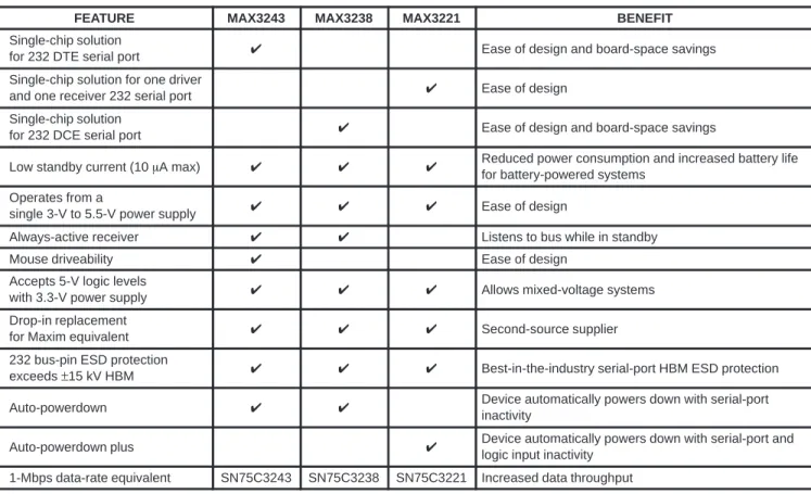
Table 3 presents important features and their respective benefits per device. TI plans to offer equivalent devices that operate at 1 Mbps for each function, and have the exact pinouts as their parent devices. These 1-Mbps devices will be SN75C3243, SN75C3238, and SN75C3221 (see Table 5). Their part numbers imply that their functionality is identical to their respective parents. To transmit at 1 Mbps, the driver output slew-rate maximum specification of 30 V/µs is violated. Thus, basically, the only two electrical differences between the MAXxxx devices and their respective 1-Mbps versions is slew rate and data rate. The faster SN75C devices are specified for 24 V/µs to 150 V/µs driver output slew rate.
Table 3. Device Features and Benefits
FEATURE MAX3243 MAX3238 MAX3221 BENEFIT
Single-chip solution
for 232 DTE serial port ✔ Ease of design and board-space savings Single-chip solution for one driver
and one receiver 232 serial port ✔ Ease of design Single-chip solution
for 232 DCE serial port ✔ Ease of design and board-space savings
Low standby current (10 mA max) ✔ ✔ ✔ Reduced power consumption and increased battery life
for battery-powered systems Operates from a
single 3-V to 5.5-V power supply ✔ ✔ ✔ Ease of design
Always-active receiver ✔ ✔ Listens to bus while in standby
Mouse driveability ✔ Ease of design
Accepts 5-V logic levels
with 3.3-V power supply ✔ ✔ ✔ Allows mixed-voltage systems Drop-in replacement
for Maxim equivalent ✔ ✔ ✔ Second-source supplier 232 bus-pin ESD protection
exceeds ±15 kV HBM ✔ ✔ ✔ Best-in-the-industry serial-port HBM ESD protection Auto-powerdown ✔ ✔ Device automatically powers down with serial-port
inactivity
Auto-powerdown plus ✔ Device automatically powers down with serial-port and
logic input inactivity 1-Mbps data-rate equivalent SN75C3243 SN75C3238 SN75C3221 Increased data throughput
Typical Design Applications
Because the 232 standard has existed since the 1960s, transmitting data via the serial bus is not new. However, offering the end-equipment manufacturer flexibility to automatically power down host and peripheral interface devices to conserve power is new to TI 232 devices and is
especially useful in battery-powered environments. In addition, as the 232 devices are powered down, one receiver always is kept active to signal the supervisory circuitry of incoming data. Most integrated circuits are designed with an external pin that can be biased appropriately to remove power from the device, thereby forcing a high-impedance state at all outputs. The MAX3xxx devices (and planned 1-Mbps siblings) also have this functionality, but go one step further by allowing the 232 device to monitor serial-port activity and power down after 30 µs of inactivity. This feature is called auto-powerdown. The MAX3238 and SN75C3238 also monitor the digital logic input side (driver inputs) and, if auto-powerdown criteria are met, the device powers down after 30 s of inactivity. This important feature is called auto-powerdown plus. For the host to communicate with the peripheral in a two-way serial-data transmission
application, conversion from TTL/CMOS to 232 levels must be accomplished. This is the sole purpose for the existence of any 232-compliant device. The onboard charge pump of these devices is capable of producing greater than ±5 V from a single 3-V power supply, thus complying with the 232 standard.
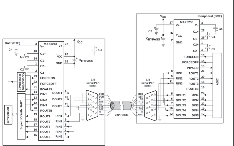
To take advantage of these powerful functions, 232 applications can be designed so that the serial port draws current from the power supply only during transmission of data. Figure 3 shows an application where the MAX3243 is used on the host (DTE) and the MAX3238 is used on the peripheral (DCE). The host can be a PC, for example, while the peripheral can be an external 56-kbps modem.Four small 0.1-µF external capacitors (C1–C4) are required to produce the 232-compliant driver output voltage levels. CBYPASS, also 0.1 µF, is recommended to decouple noise on the supply, and should be placed as close as possible to the VCC terminal.
Auto-powerdown can be deactivated by enabling the MAX3243 on the host using the RI signal from the peripheral, if it is connected to RIN2. The always-active receiver output, ROUT2B, which is electrically connected internally to RIN2, notifies the microprocessor, via the microprocessor supervisory circuitry, of impending data. Toggling RIN2 with the RI signal automatically powers up the MAX3243.
SLLA083A
9
Low-V
oltage, Single-Supply 232-Standard Interface Solutions
Figure 3 28 24 4 5 6 7 8 9 10 11 14 13 12 3 27 26 25 23 22 21 20 19 18 17 16 15 1 2 28 25 5 6 7 10 12 8 9 11 21 20 18 4 27 26 2 13 14 15 16 24 23 22 19 17 1 3 5 6 7 4 9 8 3 2 1 ASIC DSR RD RTS TD CTS DTR RI GND DCD 5 6 7 4 9 8 3 2 1 DSR RD RTS TD CTS DTR RI GND DCD
Super I/O W
ith UART Processor µ Supervisory MAX3243 + ++ + + + + ++ + 232 Serial Port DB9S C BYPASS C3 Host (DTE) C2 C1 V+ GND DOUT1 DOUT2 DOUT3 RIN1 RIN2 RIN3 RIN4 RIN5 VCC C4 C1+ C2– C2+ C1– FORCEON FORCEOFF INVALID DIN1 ROUT2B DIN2 DIN3 ROUT1 ROUT2 ROUT3 ROUT4 ROUT5 MAX3238 V– V+ V– VCC GND RIN1 DOUT1 RIN2 RIN3 DOUT2 DOUT3 DOUT4 DOUT5 C1+ C2+ C1– C2– FORCEON INVALID ROUT1 DIN1 FORCEOFF ROUT2 ROUT3 DIN2 DIN3 DIN4 DIN5 ROUT1B Peripheral (DCE) C C3 V BYPASS CC C1 C2 C4 Processor µ 232 Serial Port DB9S 232 Cable
Figure 3. Typical Host (DTE) and Peripheral (DCE) System Application
A 232 connection that requires only one driver and one receiver can be made with only three wires; one to transmit data, one to receive, and ground. No handshaking is used in this type of application, so coordination between the two units is critical. Typically, this type of application is used to allow for a large margin of error due to the lack of handshaking, and today is used widely in handheld, portable applications. Therefore, the receiver on either side must accept data as fast as the driver can transmit. In this application, the unit accepting data cannot notify the transmitter that it is going too fast.
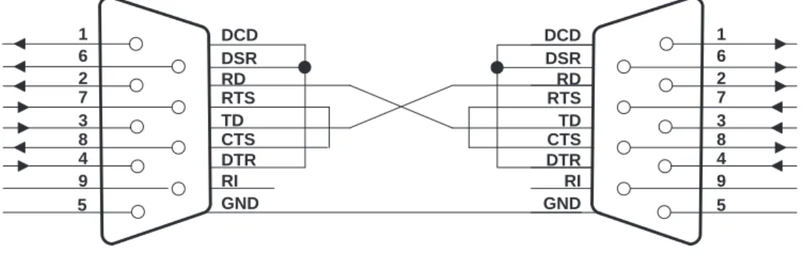
Figure 4 shows a null-modem connection for a three-wire transmission scheme, for which the MAX3221 is ideal. A null modem can connect two DTEs to make them believe handshaking is occurring.
5 6
7
4 9 8 3 2 1
DSR RD RTS TD CTS DTR RI GND DCD
5 6
7
4 9 8 3 2 1 DSR
RD RTS TD CTS DTR RI GND DCD
Figure 4. Null-Modem Wiring Diagram
The theory of operation is that the DTE thinks it is talking to a DCE rather than another DTE. TD must be connected to RD when transmitting from one DTE to the other. Signal ground also must be connected so both remote grounds are common to each DTE. The DTR signal is looped back to DSR and DCD on both sides to make the transmitting unit think that the receiving unit is ready to accept data. When DTR is asserted active, DSR and DCD immediately become active. This causes the transmitting DTE to think the virtual modem to which it is connected is ready and waiting.
Because both DTEs communicate at the same speed, handshaking is not used; thus, RTS and CTS are connected together on each side. When transmission is requested by a DTE, RTS is asserted high and gets immediate feedback that it may send data.RI is not connected on either side because this function is not used.
SLLA083A
11 Low-Voltage, Single-Supply 232-Standard Interface Solutions
Analysis of TI and Competitor Equivalent Devices
This section compares performance of the TI MAX3243 and that of a competitor’s ’3243.
Specifically, driver output voltage, supply current, and slew rate are examined closely to provide a good understanding of the charge-pump and output-driver performance, and an estimate of the expected supply current. All measurements are taken at room temperature with a 5-kΩ load resistor at the driver output. The analysis was performed only on the ’3243 device, but similar results can be expected from the MAX3238 and MAX3221.
Driver Output Voltage
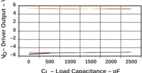
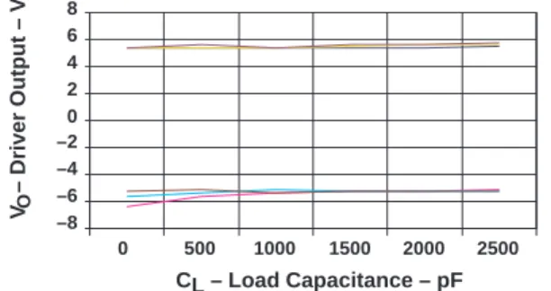
Figures 5 and 6 indicate the performance of the onboard charge pump by displaying the
competitor’s ’3243 driver output voltage at different data rates and different numbers of switching outputs. Figures 7 and 8 show the driver output voltage of the TI MAX3243. This data was obtained while switching one output at 250 kbps, switching two outputs at 120 kbps, and switching three outputs at 50 kbps. Both devices meet the minimum 232 driver output voltage requirement (VOH = +5 V and VOL = –5 V).
–6 –4 –2 0 2 4 6
0 500 1000 1500 2000 2500
V – Driver Output – V
CL – Load Capacitance – pF
O
Figure 5. Competitor’s Device Output Voltage vs CL (VCC = 3.3 V)
–8 –6 –4 –2 0 2 4 6 8
0 500 1000 1500 2000 2500
CL – Load Capacitance – pF
V – Driver Output – VO
–6 –4 –2 0 2 4 6
0 500 1000 1500 2000 2500
CL – Load Capacitance – pF
V – Driver Output – VO
Figure 7. TI Device Output Voltage vs CL (VCC = 3.3 V)
–8 –6 –4 –2 0 2 4 6 8
0 500 1000 1500 2000 2500
CL – Load Capacitance – pF
V – Driver Output – VO
Figure 8. TI Device Output Voltage vs CL (VCC = 5 V)
Supply Current
Figures 9 and 10 show the supply current of the competitor’s ’3243 device while varying data rates and number of switching outputs. Figures 11 and 12 show TI MAX3243 device supply current. The TI MAX3243 slightly outperforms the competing device at the highest current, which is at 250 kbps, 2500-pF load, and one switching-output driver.
7 12 17 22 27 32 37
0 500 1000 1500 2000 2500
I – Supply Current – mA
1 2
3 4 5
CL – Load Capacitance – pF
1 – 250 kbps and one output switching 2 – 120 kbps and two outputs switching 3 – 50 kbps and three outputs switching 4 – 120 kbps and one output switching 5 – 50 kbps and one output switching
C
SLLA083A
13 Low-Voltage, Single-Supply 232-Standard Interface Solutions
CL – Load Capacitance – pF
1 – 250 kbps and one output switching 2 – 120 kbps and two outputs switching 3 – 50 kbps and three outputs switching 4 – 120 kbps and one output switching 5 – 50 kbps and one output switching
7 12 17 22 27 32 37
0 500 100 1500 2000 2500 1 2
3 4
5
I – Supply Current – mAC
Figure 10. Competitor’s Device Supply Current vs CL (VCC = 5 V)
CL – Load Capacitance – pF
7 12 17 22 27 32 37
0 500 1000 1500 2000 2500 1 2
3 4
5
1 – 250 kbps and one output switching 2 – 120 kbps and two outputs switching 3 – 50 kbps and three outputs switching 4 – 120 kbps and one output switching 5 – 50 kbps and one output switching
I – Supply Current – mAC
Figure 11. TI Device Supply Current vs CL (VCC = 3.3 V)
CL – Load Capacitance – pF
1 – 250 kbps and one output switching 2 – 120 kbps and two outputs switching 3 – 50 kbps and three outputs switching 4 – 120 kbps and one output switching 5 – 50 kbps and one output switching
7 12 17 22 27 32 37
0 500 1000 1500 2000 2500 1 2
3 4 5
I – Supply Current – mAC
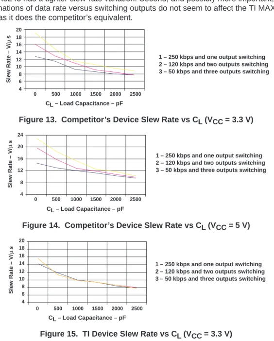
Slew Rate
The 232 standard specifies the slew rate of the output driver to be no greater than 30 V/µs. With other specifications, the maximum limit on slew rate ensures that any 232-compliant connection behaves as a lumped load rather than as a transmission line. Therefore, it is critical that an output driver not exceed this slew-rate specification limit for true 232 compliance.
Figures 13 and 14 show the slew-rate performance of the competitor’s ’3243 at different
combinations of data rates and numbers of switching outputs. Figures 15 and 16 show the slew rate of the TI MAX3243. From these graphs, two important observations can be made. First, the TI MAX3243 has a tighter slew-rate variation. Second, and possibly more important, various combinations of data rate versus switching outputs do not seem to affect the TI MAX3243 as much as it does the competitor’s equivalent.
4 6 8 10 12 14 16 18 20
0 500 1000 1500 2000 2500
Slew Rate – V/
µ
s
CL – Load Capacitance – pF
1 – 250 kbps and one output switching 2 – 120 kbps and two outputs switching 3 – 50 kbps and three outputs switching
Figure 13. Competitor’s Device Slew Rate vs CL (VCC = 3.3 V)
Slew Rate – V/
µ
s
CL – Load Capacitance – pF
1 – 250 kbps and one output switching 2 – 120 kbps and two outputs switching 3 – 50 kbps and three outputs switching
4 8 12 16 20 24
0 500 1000 1500 2000 2500
Figure 14. Competitor’s Device Slew Rate vs CL (VCC = 5 V)
Slew Rate – V/
µ
s
CL – Load Capacitance – pF
1 – 250 kbps and one output switching 2 – 120 kbps and two outputs switching 3 – 50 kbps and three outputs switching
4 6 8 10 12 14 16 18 20
SLLA083A
15 Low-Voltage, Single-Supply 232-Standard Interface Solutions
Slew Rate – V/
µ
s
CL – Load Capacitance – pF
1 – 250 kbps and one output switching 2 – 120 kbps and two outputs switching 3 – 50 kbps and three outputs switching
4 8 12 16 20 24
0 500 1000 1500 2000 2500
Figure 16. TI Device Slew Rate vs CL (VCC = 5 V)
Figures 17–20 further strengthen the observation regarding the TI device’s better slew-rate performance compared to the competitor’s equivalent. These data points were generated while switching one output at 250 kbps, switching two outputs at 120 kbps, and switching three outputs at 50 kbps. From top to bottom, curves in Figures 17–20 represent capacitive loading of 0 pF, 500 pF, 1000 pF, 1500 pF, 2000 pF, and 2500 pF, respectively. The nearly flat slew-rate response of the TI MAX3243 is superior to the competitor’s device.
4 8 12 16 20
250 120 50
Data Rate – kbps
Slew Rate – V/
µ
s
Figure 17. Competitor’s Device Slew Rate vs Data Rate(VCC = 3.3 V)
Data Rate – kbps
Slew Rate – V/
µ
s
4 8 12 16 20 24
250 120 50
Data Rate – kbps
Slew Rate – V/
µ
s
4 8 12 16 20
250 120 50
Figure 19. TI Device Slew Rate vs Data Rate(VCC = 3.3 V)
Data Rate – kbps
Slew Rate – V/
µ
s
4 8 12 16 20 24
250 120 50
SLLA083A
17 Low-Voltage, Single-Supply 232-Standard Interface Solutions
Conclusion
A summary of the laboratory experiments is shown in Table 4. TI MAX3243, MAX3238, and MAX3221 integrated 232-compliant solutions offer superior performance for single, low-voltage applications that operate from 3 V to 5.5 V. Comparison of the TI MAX3243 with the leading 232-compliant competitor’s equivalent shows the same, or better, performance from the charge pump that provides the necessary voltages for the output driver.
Table 4. Summary Comparison of TI MAX3243 and Competitor’s ’3243
TEST TEST CONDITIONS TI
MAX3243
COMPETITOR’S
’3243 COMMENTS
Output voltage (VO) vs
VCC = 5 V, CL = 2500 pF, One output switching at 250 kbps
VOH = 5.2 V VOL = –5.1 V
VOH = 6.4 V
VOL = –5.5 V Both meet the minimum 232 requirement for VO vs
Load capacitance (CL) VCC = 3.3 V, CL = 2500 pF, VOH = 5.5 V VOH = 5.6 V
232 requirement for VO (VOH > 5 V and VOL < –5 V). Load ca acitance (CL) CC , L ,
One output switching at 250 kbps
OH VOL = –5.0 V
OH
VOL = –5.5 V (VOH > 5 V and VOL < –5 V). Supply current (ICC)
vs
VCC = 5 V, Cload = 2500 pF,
One output switching at 250 kbps ICC = 35.75 mA ICC = 38.25 mA Reduced power consumption vs
Load capacitance (CL) One output switching at 250 kbpsVCC = 3.3 V, Cload = 2500 pF, ICC = 36.25 mA ICC = 38.25 mA on TI MAX3243
Slew rate
VCC = 5 V Slew-rate variationis 8.9 V/µs. Slew-rate variationis 13.5 V/µs.
TI MAX3243 has better Slew rate
VCC = 3.3 V Slew-rate variationis 7.6 V/µs. Slew-rate variationis 11.4 V/µs. slew-rate performance.
Orderable part numbers of devices soon to be available are listed in Table 5.
Table 5. Orderable Part Numbers for New TI 232-Compliant 3-V to 5.5-V Devices
PART
NUMBER PACKAGES AVAILABLE
TEMPERATURE RANGE
MAXIMUM DATA RATE
PIN COUNT MAX3243C Wide-SOIC, SSOP, and TSSOP 0°C to 70°C 250 kbps 28 MAX3243I Wide-SOIC, SSOP, and TSSOP –40°C to 85°C 250 kbps 28 SN75C3243 Wide-SOIC, SSOP, and TSSOP 0°C to 70°C 1 Mbps 28 SN65C3243 Wide-SOIC, SSOP, and TSSOP –40°C to 85°C 1 Mbps 28 MAX3238C Wide-SOIC, SSOP, and TSSOP 0°C to 70°C 250 kbps 28 MAX3238I Wide-SOIC, SSOP, and TSSOP –40°C to 85°C 250 kbps 28 SN75C3238 Wide-SOIC, SSOP, and TSSOP 0°C to 70°C 1 Mbps 28 SN65C3238 Wide-SOIC, SSOP, and TSSOP –40°C to 85°C 1 Mbps 28 MAX3221C SSOP and TSSOP 0°C to 70°C 250 kbps 16 MAX3221I SSOP and TSSOP –40°C to 85°C 250 kbps 16 SN75C3221 SSOP and TSSOP 0°C to 70°C 1 Mbps 16 SN65C3221 SSOP and TSSOP –40°C to 85°C 1 Mbps 16
Reference
Texas Instruments and its subsidiaries (TI) reserve the right to make changes to their products or to discontinue any product or service without notice, and advise customers to obtain the latest version of relevant information to verify, before placing orders, that information being relied on is current and complete. All products are sold subject to the terms and conditions of sale supplied at the time of order acknowledgment, including those pertaining to warranty, patent infringement, and limitation of liability.
TI warrants performance of its semiconductor products to the specifications applicable at the time of sale in accordance with TI’s standard warranty. Testing and other quality control techniques are utilized to the extent TI deems necessary to support this warranty. Specific testing of all parameters of each device is not necessarily performed, except those mandated by government requirements.
Customers are responsible for their applications using TI components.
In order to minimize risks associated with the customer’s applications, adequate design and operating safeguards must be provided by the customer to minimize inherent or procedural hazards.
TI assumes no liability for applications assistance or customer product design. TI does not warrant or represent that any license, either express or implied, is granted under any patent right, copyright, mask work right, or other intellectual property right of TI covering or relating to any combination, machine, or process in which such semiconductor products or services might be or are used. TI’s publication of information regarding any third party’s products or services does not constitute TI’s approval, warranty or endorsement thereof.