Design and Simulation of an Oblique
Suspender MEMS Variable Capacitor
H. Nabovati
, K. Manezhad
1, H. Keshmiri
1and A. Nabovati
2This paper presents the results on the development of a novel micromachined parallel plate tunable capacitor with a wide tuning range. Dierent from conventional parallel plate capacitors, this novel tunable capacitor consists of one suspended top plate, suspending with four oblique arms and one bottom xed plate. These oblique arms increase the length of the cantilevers, in order to cause more deection and, hence, increase the tuning range of the capacitor for constant bias voltage. Applying a DC voltage between two plates provides electrostatic actuation for capacitance tuning. According to electromagnetic simulation, a tuning range of 146% has been achieved with a 1.7 volt bias voltage. An empirical behavioral model is extracted from simulated
y parameters of the structure.
INTRODUCTION
The increasing demand for smaller and more ca-pable portable phones, notebook computers, global positioning system receivers and remote sensors, has spawned an explosive growth in wireless technology. As the demand increases, more ecient use of an allocated spectral frequency range and much more capable implantation technologies are required. In recent years, MEMS (Micro Electromechanical Sys-tems) technology has begun to be used in wireless communication systems, to improve the performance of existing devices based on structures or operational principles.
At present, the ultimate miniaturization of super heterodyne transceivers is limited mainly by the need for numerous o-chip frequency selective passive com-ponents, such as variable capacitors and inductors. A variable capacitor is the basic component of a Voltage Controlled Oscillator (VCO) used in frequency syn-thesizers, which generates the local oscillator signals. Currently, such VCO's are implemented using o-chip inductors (with a Q of at least 30) combined with
o-chip voltage tunable varactor diodes (with a Q of
*. Corresponding Author, Department of Electrical Engi-neering, Ferdowsi University of Mashhad, Mashhad, I.R. Iran.
1. Department of Electrical Engineering, Ferdowsi Univer-sity of Mashhad, Mashhad, I.R. Iran.
2. Department of Mechanical Engineering, University of New Brunswick, Canada.
at least 40). Recent demonstrations of voltage tun-able capacitors comprised of micromachined, movtun-able metal plates, now oer substantial improvements over varactor diodes. Compared with solid state varactors, micromachined variable capacitors have the advantage of lower loss, a higher quality factor and potentially greater tuning range [1-4].
The recent applications of MEMS technologies in voltage tunable capacitors use two methods, the trothermal method and electrostatic method. The elec-trothermal method uses the deection of supporting arms, due to the dierent axial strain of a compound beam when a temperature dierence is exerted. This method has a wide tuning range, but is slow and needs more space. In the electrostatic method, capacitance is tuned by varying the distance between two plates using an electrostatic force caused by a bias voltage. The desired capacitance is accomplished by fast tuning and small space, but, the theoretical tuning range is limited by 150% [5]. Among all the MEMS tunable capacitors developed before, the parallel plate conguration with electrostatic actuation is the most commonly used [4,5]. The main eort applied in designing these structures is in developing tunability and decreasing the structure loss that will lead to a higher quality factor.
In the present work, the development of a novel MEMS electrostatically tunable capacitor has been studied using full wave electromagnetic simulation. This new design keeps the simplicity of conventional two parallel plate congurations, while providing a much wider tuning range. An empirical behavioral model is extracted that can be dened by circuit
simulator software and can be scaled according to device dimensions.
The new tunable capacitor can be fabricated using a standard surface micromachined process and can be monolithically integrated with other RF circuits.
MECHANICAL DESIGN
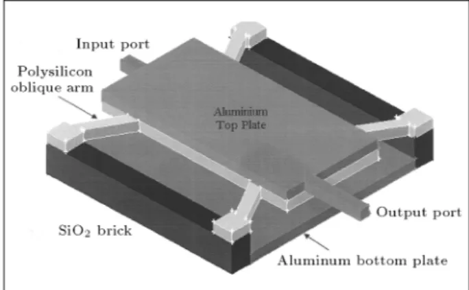
As schematically shown in Figure 1, the top plate of the capacitor has been suspended using four oblique cantilever beams. Using the basic mechanics been suspended using four oblique cantilever beams. Using the basic mechanics of solids, it can be shown that the deection of a cantilever beam, which has been subjected to a concentrated load at its end, can be calculated as below [6]:
= Fl
3
3YI
; (1)
in whichF,l,I andY are applied force, beam length,
moment of inertia of beam cross section and Young's modulus of elasticity, respectively. It means that the deection is a cubic function of beam length, so, this novel design using oblique beams, takes advantage of this property and produces a 283% increase in the de-ection of the beams, in comparison with conventional normal beams. It means that a lower bias voltage is needed for a constant tuning range of the capacitor.
When a DC bias voltage is applied between two plates, with an initial gap size of 1.2 m at V = 0,
an attractive electrostatic force is generated between them and the top plate moves toward the xed one, until equilibrium between electrostatic and mechanical forces is achieved. By neglecting the ring eect, the capacitance of the capacitor, which has been formed between the two plates, can be written as:
C=" A
x
; (2)
where x is the distance between two plates, A is the
plate surface area and " is the permittivity of the air
Figure1. Perspective of the designed structure.
gap. When the bias voltage,V, is applied, the stored
electrical energy will be:
E= 12CV 2=
"AV 2
2x
: (3)
Assuming a potential eld, the electrostatic force be-tween two plates can be calculated as:
F = @E
@x
; (4)
in which x is the distance between two plates and
is equal to x 0
and where is the deection of
the beams. The mechanical force exerted on the top plate, due to the deection of the four beams, can be calculated using the following equation:
F = 12 EI
l
3 = 12 EI(x
0 x) l
3
; (5)
whereEis the Young's module,lis the arm length,x 0
is the initial distance and I is the moment of inertia
for the cantilever beam, which could be calculated according to the following equation;
I = wt
3
3 ; (6)
in which w is the beam width and t stands for its
thickness. When the equilibrium between electrostatic and mechanical forces is achieved, the top plate will be in force equilibrium, thus;
12EI(x 0 x) l 3 = "AV 2 2x 2 : (7)
It is important to note that the corresponding value of V at x = 2=3x
0 is the critical point and is called
the pull-in voltage [5]. If V is increased beyond this
value, no equilibrium can be achieved and the top plate will move toward the bottom one until they snap into contact. This phenomenon is called the pull-in eect. Thus, according to Equation 6, theoretically, the maximum capacitance of the variable capacitor is 150% of its initial value atV = 0.
Figure 2 shows the distance of two plates versus the applied bias voltage. The eect of an oblique beam in increasing the deection is vividly obvious. The initial distance is assumed as 1.2 m and the
pull-in eect has occurred at 1.7 V for the oblique beams. At this point, the distance between two plates reaches 0:8m.
ELECTROMAGNETICSIMULATION
The full wave electromagnetic simulation of the ca-pacitor has been done using MEM Research EM3DS 6.1 [7,8]. In the simulation, a box with the size of
Figure2. Variation of gap distance verses bias voltage L= 42m,t= 0:5m,w= 7 m,A= 200200m
2.
400400m is used. The top wall of the structure is
assumed to be innity dielectric and the bottom wall is a perfect conductor.
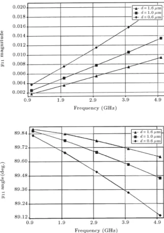
After a full wave analysis, y parameters of the
structure are extracted in the frequency range from 1 GHz to 5 GHz for dierent distances between the capacitor plates. Figures 3 and 4 represent simulation results fory
11 and y
22 when the distances are equal to
Figure3. Magnitude and angle ofy
11for variable gap
distances (0.6, 1 and 1.6m).
0.6, 1 and 1.6m, respectively.
The structure, as schematically shown in Figure 5, consists of 6 dierent layers. The substrate is assumed to be lossy silicon with a relative dielectric constant of 11.8 and a conductivity of 0.0033S/m. The thickness of this layer is 1000m.
The substrate is assumed to be coated with 1.5 m thick dielectric with a relative dielectric
con-stant of 7.6 (corresponding to silicon nitride).
The capacitor bottom plate is realized with 0.5 m thick aluminum with a resistivity of 3
10 8 m, which is deposited on the dielectric layer.
The top plate is suspended using two dielectric bricks with a relative dielectric constant of 3.9 (corresponding to silicon dioxide). The top layer of the variable capacitor consists of two layers. The rst one, which is suspended by cantilever arms, is assumed to be polysilicon with a 0.5m thickness and a resistivity of
310
5m. The next layer has been embedded over
the polysilicon layer and is assumed to be aluminum with a thickness of 0.5m.
The complete structure is schematically shown in Figure 1. The results of the electromagnetic simulation are used to extract an equivalent circuit model for the voltage tunable capacitor. Moreover, the quality
Figure4. Magnitude and angle ofy
12for variable gap
Figure5. Cross section of the structure.
Figure6. Quality factor for variable gap distances (0.6, 1
and 1.6m).
factor and current density of MEMS have been calcu-lated.
Figure 6 shows, respectively, the EM simulated quality factor of the structure with gaps of 0.6, 1 and 1.6 m between the two plates. The quality factor
exceeds 460 in 1GHz, which is sucient for almost every communication application.
Figure 7 presents the current density distribution over the surface of the top and bottom plates. For this simulation, the input and output ports have been terminated with short circuits and the calculation was done in 3GHz. The calculation was done when the input port was stimulated with a 1-volt signal.
EMPIRICAL BEHAVIORALMODELING
Figure 8 presents an equivalent circuit model for a variable MIM capacitor. The network has been selected for accurate broadband modeling of the struc-ture.
Figure 7. Current density contour in two plates.
Figure 8. Equivalent circuit for designed variable
capacitor.
In this circuit,Cmodels the capacitance between
two ports and R stands for capacitance leakage. These two parameters present an intrinsic model of the MEMS.
Three parasitic elements present the capacitance extrinsic model of the MEMS. C
p1 and C
p2 model
the parasitic capacitance of the structure and R p1
corresponds to the power dissipation at the input port. The output dissipation is negligible.
Using the results of full wave analyses, for dif-ferent distances between the plates, the equivalent circuit parameters are extracted and scaled according to the distance. The y parameters are used for this
purpose. The procedure is straightforward and has been presented in Equations 7 to 11;
R=
1 Re(y
12)
; (8)
C= Im( y
12)
2f
R P1=
1 Re(y
11) 1 R
; (10)
C
P1= Im( y
11)
2f
C ; (11)
C
P2= Im( y
22)
2f
C : (12)
The results are summarized in Figures 9 to 12 and the values of the intrinsic and parasitic elements of the equivalent circuit are reported for various device dimensions. It is obvious that the variation of para-sitic capacitance according to gap distance is almost negligible. The thickness and permittivity of the substrate coating layer and substrate conductance are the most important parameters, which control parasitic capacitances.
According to these calculations, a behavioral in-trinsic model is extracted, which denes these elements as a function of gap distance.
Figure9. Modeled and simulated values of intrinsic
capacitance.
Figure10. Modeled and simulated values of intrinsic
resistance.
Figure11. Simulated values of parasitic capacitances
verses distance of two plates.
As a classic parallel plate capacitance, the vari-ation of the capacitance, according to the inverse of the distance (1=x), is assumed to be linear. Because
of parasitic eects, e.g. fringing, the intrinsic capac-itor has a 29.5 fF oset when 1=x tends to zero.
Equation 13 is presented to describe the capacitance variation. The parameter extraction algorithm is realized by MATLAB 6.5 software from Mathworks.
C(fF) = 29:5 + 310 :9 x
: (13)
The resistance,R, is described as a quadratic function
of the gap distance in the following equation:
R(K) = 16:6x 2+ 12
:8x 2:8: (14)
In Figures 9 and 10, the values predicted by these behavioral models are compared with the simulation results of the structure. The gures show very good agreement between two sets of results. The model error is less than 0.25% for resistance and 0.57% for capacitance evaluating.
Figure12. Simulated values of parasitic resistance.
Figure13. Variation of intrinsic capacitance versus bias
voltage.
Figure 13 presents the variation of intrinsic capac-itance versus applied bias voltage for both an oblique beam and a normal beam. As expected, the tuning range is limited by the pull-in eect, which is predicted to be about 146%, but, the eect of the oblique beams in decreasing the pull-in voltage, from 2.86 V to 1.7 V, is vividly obvious.
MODEL VERIFICATION
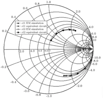
A scattering parameters prediction has been used for model verication. The equivalent circuit model is dened in APLAC, an object-oriented simulator and design tool, as a user dened model. The software was chosen because of its powerful RF module and simplicity [9].
Thes-parameters are calculated at each gap
dis-tance for variable bias points. The result was compared with MEMS scattering parameters extracted from the EM simulation and shows good agreement between the two groups of parameters. The EM simulated
Figure 14. Comparison of scattering parameters.
and equivalent circuit parameters are presented on the Smith chart. Figure 14 shows the agreement between the parameters for a gap distance equal to 1 m.
The comparison between the two sets of scattering parameters was done by an error estimation algorithm. The results show that there is 2.6% and 2.9% error in determining s
11 and s
12 arguments and a 0.02 radian
dierence between the phases.
CONCLUSION
A new oblique suspender voltage tunable MEMS ca-pacitor has been designed and electromagnetically sim-ulated. Although the tuning range of the capacitance is limited by the pull-in eect, by using oblique arms, the beam deection was increased and so, therefore, was the tunability of the capacitance. A behavioral intrinsic model and an equivalent circuit are extracted from EM simulations. The modeling error for all levels of modeling is less that 1%.
ACKNOWLEDGMENT
The authors wish to thank Professor Marco Farina from MEM Research for his guidance and for providing the EM3DS tool to carry out this work. The support of the Microelectronic Research Laboratory at the Ferdowsi University of Mashhad is also acknowledged.
REFERENCES
1. Nguyen, C.T. \Communication application of miro-electromechanical systems",Proceedings, 1998 Sensors Expo., San Jose, CA, pp 447-455 (May 1998).
2. Katehi, L.P.B., Harvey, J.F. and Brown, E. \MEMS and Si micromachined circuits for high-frequency
ap-plications",I IEEE Transaction on Microwave Theory and Techniques,50(3), pp 858-866 (March 2002).
3. De Los Santos, H.J.,RF MEMS Circuit Design, Artech House, Boston (2002).
4. Bushyager, N., Tentzeris, M.M., Gatewood, M.M. and DeNatale, L. \A novel adaptive approach to modeling MEMS tunable capacitors using MRTD and FDTD techniques", Microwave Symposium Digest, 2001 IEEE MTT-S International,3, pp 2003-2006
(20-25 May 2001).
5. Zou, J., Liu, C., Schutt-Aine, J., Chen, J. and Kang, S. \Development of a wide tuning range MEMS tunable capacitor for wireless communication systems",
Elec-tron Devices Meeting, 2000, IEDM Technical Digest. International, pp 403-406 (Dec. 2000).
6. Beer, F.P. and Johnston, E.R.,Mechanics of Materials, McGraw Hill (1992).
7. EM3DS 6.1 User Manual Release 1.5, MEM Research (May 2003).
8. Farina, M. and Rozzi, T. \A 3-D integral equation-based approach to the analysis of real-life MICs-application to microelectromechanical systems",IEEE Transaction on Microwave Theory and Techniques,
49(12) pp 2235-2240 (December 2001).
9. APLAC 7.90 User Manual, APLAC Solution Corpo-ration (2003).