Sharif University of Technology
Scientia IranicaTransactions D: Computer Science & Engineering and Electrical Engineering http://scientiairanica.sharif.edu
Modeling of a PIN diode RF switch for recongurable
antenna application
J. Kumar, B. Basu
, and F.A. Talukdar
Electronics and Communication Engineering Department, National Institute of Technology Silchar, Silchar, Cachar-788010, Assam, India.
Received 28 February 2017; received in revised form 6 June 2017; accepted 6 January 2018
KEYWORDS Frequency recongurable antenna;
PIN diode modeling; Microstrip antenna; SAR investigation; UWB to narrowband switching.
Abstract.The paper presents a procedure to model a PIN diode RF switch using a full-wave EM solver, HFSS. It utilizes the switch to build a simple partial ground plane antenna with an omnidirectional radiation pattern. The proposed antenna has the ability to tune the frequency from the ultra-wideband to narrowband mode. The frequency recongurability is accomplished by incorporating a rectangular slot resonator and a PIN diode RF switch embedded in the partial ground plane. The antenna demonstrates 10 dB impedance bandwidth from 500 MHz to 6 GHz in the ultra-wideband mode and 1.125 GHz to 2 GHz in the narrowband mode. A parasite is stacked in the ground plane to improve the impedance matching, and a rectangular slot is fused to explore the bandwidth-limiting possibility of the antenna. The optimization of the antenna is done by a full-wave EM solver, HFSS; moreover, Specic Absorption Rate (SAR) of the antenna is examined using the equivalent at tissue phantom. A prototype of the proposed antenna is fabricated, and execution is accepted by measured results. The proposed antenna has a simple and miniature structure, low SAR (0.41 W/kg), an omnidirectional pattern, and low cross polarization (< 15 dB in E-plane and < 30 dB in H-plane).
© 2019 Sharif University of Technology. All rights reserved.
1. Introduction
The printed monopole antennas have drawn much attention to the variety of communication systems owing to their omnidirectional radiation pattern, Ultra-Wide Bandwidth (UWB), low prole, and ease of fabrication and integration [1]. By using dierent congurations, numerous printed monopole structures, including rectangular and circular shapes, have been
*. Corresponding author. Tel.: +91 8474 801 115
E-mail addresses: jayendra854330@gmail.com (J. Kumar); basu banani@yahoo (B. Basu); fatalukdar@gmail.com (F.A. Talukdar)
doi: 10.24200/sci.2018.20110
presented in the literature [2-9]. The aptness of the UWB antennas is to replace multiple antennas of a multi-radio system by covering dierent narrowband services as WLAN, WiMax, GSM, UMTS, Wi-Fi, WMTS, and MICS through a single antenna. However, the design and implementation of UWB systems are complicated due to the signicant thermal agitation noise and the requirement of a higher signal-to-noise ratio.
The future communication systems, such as Soft-ware Dened Radio (SDR) and Cognitive Radio (CR), are yet under development, and there are no clear standards for them [10]. According to the very First CR standard IEEE 802.22 for Wireless Regional Area Network, sensing and database access are the two prime requirements [11,12]. An antenna should
quency recongurable antenna was presented in [17], which placed two PIN diode RF switches in the radiator to operate at LTE 20 (791-862 MHz) and LTE 7 (2500-2690 MHz) bands. Similarly, in [18-21], narrowband frequency recongurability was achieved by incorporating RF switches between the current paths. In the second case, electronically controlled slot resonator(s) of rectangular shape, L-shape or of any random shape is incorporated into the radiator or ground plane to achieve the frequency agility. The second mechanism is found useful for wideband and ultra-wideband frequency recongurations. In [22], an optimized slot resonator integrated with a varac-tor diode was incorporated in the radiavarac-tor to obtain the ultra-wideband to narrowband tunable frequency recongurability. In [23], PIN diode integrated slot resonators were embedded in the ground plane to achieve the ultra-wideband to narrowband frequency reconguration. However, the second mechanism is also observed for multiband and narrowband frequency recongurability [24,25]. The work demonstrates the modeling of the PIN diode RF switch in HFSS and its application to frequency reconguration from ultra-wideband to narrowband using the second mechanism. In spite of the fact that the recongurable an-tennas are well known, a comprehensive explanation is required to elaborate on the design process using the commercially available EM solver. This paper presents a brief description of modeling a PIN diode RF switch to be utilized for recongurable antenna applications. We have studied the performance variations of an ideal switch and a practical switch for a partial ground plane monopole antenna. Further, the antenna structure is optimized through rigorous simulation to achieve wider bandwidth and better impedance matching. In the narrowband mode, the antenna operates in the WMTS band (1.395-1.432 GHz); hence, the SAR of the antenna is examined and noticed under the safety level. The prototype of the antenna is fabricated and simulated, and measured results are found in very good agreement. Following the introduction, the rest of the paper is organized as follows. The modeling of the PIN diode RF switch is explained in Section 2. Antenna design
they are costlier and require higher operating voltage. However, the FETs have low power consumption, yet suer from higher loss and poor linearity. The PIN diode-based RF switches are cheaper and oer low-loss operation. The limitation of a PIN diode switch is that a forward dc current is required to switch the diode in the ON state, leading to poor radiation eciency. In this section, the modeling of a PIN diode RF switch is graphically demonstrated using HFSS. Insertion loss and isolation are the key parameters of RF switches. These parameters depend not only on the devices but also on the congurations of biasing circuits. For diode-based RF switches, series and shunt connected diodes are the most commonly used congurations [28]. However, due to the ease of integration, most of the recongurable antennas reported in the literature have used the series conguration of the RF switch and external biasing circuits. Here again, BAP64-02 pin diode-based series conguration of the RF switch is utilized. The conguration of the RF switch [28] and the insertion and isolation loss are shown in Figure 1. The RF switch is simulated by Advanced Design System (ADS).
The equivalent circuits of a PIN diode RF switch in ON and OFF states are shown in Figure 2(a) and (b), respectively [28]. The equivalent circuits of the PIN diode RF switch in ON and OFF states can be modeled in HFSS by assigning \Lumped RLC" boundary to the or 3D-structures [29]. In the HFSS, a single 2D-or 3D-structure can be modeled as a single lumped element or a parallel combination of lumped elements (resistor, inductor, and the capacitor). Similarly, for a series combination of the n-number of elements, n-number of interconnected structures are required. In the ON state, the equivalent circuit consists of a series combination of two DC blocking capacitors, an inductor, and a resistor.
Similarly, the OFF-state equivalent circuit has a series combination of four dierent elements. Thus, four interconnected 2D- or 3D-structures are required to model a PIN diode RF switch, as shown in Fig-ure 2(c). Now, to model a structFig-ure as a lumped component, \Lumped RLC" boundary is assigned to
Figure 1. Congurations of the PIN diode RF switches: (a) Conguration and (b) performance.
Figure 2. Modeling of the PIN diode RF switch in HFSS: (a) RF switch ON-state equivalent circuit, (b) RF switch OFF-state equivalent circuit, (c) four interconnected 2D-structures representing switch model in HFSS, and (d) \Lumped RLC" boundary assignment to a 2D-structure (all dimensions in mm).
each structure. To assign the boundary, the direction of the current ow should be dened, as shown in Figure 2(d). To model the PIN diode RF switch in the ON state, two blue 2D-structures are assigned as a capacitor (C, blue), pink as an inductor (L, pink), and yellow as a resistor (R or R//C, yellow),
as shown in Figure 2(c). In the OFF state, both resistor and capacitor values are assigned to the yellow 2D-structure, and the other structures are kept as they are. Further, the lumped RLC assignment can be modied simply through \boundaries" in Project three. However, the size of 2D-structures is taken by
Figure 3. (a) Basic partial ground plane monopole antenna conguration and (b) input reection parameter versus length (L) of the partial ground plane (all dimensions are in mm).
considering the size of practical components, ease of soldering, and integration of the diode biased lines. 3. Antenna design and analysis
A monopole rectangular microstrip antenna is chosen as a basic radiating structure (Figure 3(a)) on account of its ultra-wide bandwidth and good radiation char-acteristics [2-9]. The antenna is built on FR4 Epoxy dielectric substrate with dielectric constant of 4.4, dielectric loss tangent of 0.018, thickness of 1.57 mm. The antenna is excited via 50 inset feed through an SMA connector.
The length of the partial ground (L) is opti-mized to obtain ultra-wide bandwidth, as shown in Figure 3(b). Due to better impedance matching at the lower cut-o frequency, L = 6 mm is chosen for the nal design. It is clearly observed that the ground plane length (L = 6 mm) shifts the lower edge of the frequency band to its minimum, preserving the length of the current path and presenting the best input scat-tering parameter (S11) at the lower cut-o frequency (Figure 3). The frequency recongurability is realized by integrating a bandstop lter in the partial ground, as shown in Figure 4. The bandstop lter comprises g=8 (g is the guided wavelength) rectangular slot
resonator and an RF switch embedded in the center
Figure 4. Conguration of the proposed antenna: (a) Top view and (b) bottom view (all dimensions are in mm).
Figure 5. The g=8 resonator incorporated in the ground
plane of the UWB antenna exhibiting the contraction of the bandwidth with increasing slot length.
of the resonator. It is shown in Figure 5 that as the length of the CPW bandstop resonator increases, the bandwidth of the antenna becomes narrower. In this way, by integrating the lter and antenna together, the narrowband operation is obtained.
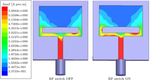
The antenna operates in the ultra-wideband mode as the lter is disabled by placing the switch in the ON state and yields single band operation as the lter is enabled by turning the switch to the OFF state. The bandstop behavior of the lter can be explained by the surface current distribution, as shown in Figure 6.
When the switch is in the ON state, it provides a direct path to the current causing the antenna to operate in the ultra-wideband mode. As the switch is turned OFF, the current path through g=8
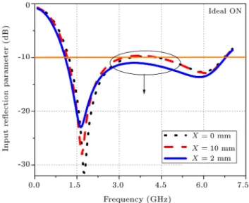
res-onator becomes dominant, and the antenna operates in the narrowband mode. To obtain better impedance matching, a parasite is loaded on the ground, as shown in Figure 4. The length (X) of the parasite is optimized to improve the S11 parameter, as shown in Figure 7. However, there is no signicant change in the
Figure 6. Surface current distribution on the partial ground plane with an embedded slot resonator at 1.43 GHz: (a) Switch in the ideal ON state and (b) switch in the ideal OFF state.
Figure 7. Input reection parameter of the proposed antenna for dierent lengths of loaded parasite (all dimensions are in mm).
impedance matching characteristics of the narrowband mode.
The antenna operates in the ultra-wideband mode as the lter is disabled by placing the switch in the ON state, and it yields single band operation as the lter is enabled by turning the switch in the OFF state. The bandstop behavior of the lter can be explained by the surface current distribution, as depicted in Figure 6. When the switch is in the ON state, a direct path is provided to the current, causing the antenna to operate in the ultra-wideband mode.
The 10 dB impedance bandwidth of the pro-posed antenna is investigated for the ideal switch and a practical PIN diode RF switch, as depicted in Figure 8. A perfect electric conductor is used to realize the ideal switch in the ON state and open
Figure 8. Input reection parameter of the proposed antenna for the ideal switch and practical switch.
circuit in the OFF state. A practical PIN diode is modeled as a 1 resistor connected in the series with 0.6 nH inductor. In the OFF state, the diode is modeled as a 0.6 nH inductor connected in the series with a parallel combination of 0.5 pF capacitor with a 20 K resistor [30]. Two capacitors of 1 F are placed back and forth to the PIN diode to provide the RF connectivity and block the dc. For a practical switch, the antenna exhibits narrower bandwidth in the narrowband mode and better impedance matching in the UWB mode over an ideal switch. The inductance, ON-state resistance, and OFF-state capacitance are taken from the technical data sheet of BAP65-02, 115 PIN diodes.
UWB antennas exhibits a number of advantages: high-rate data support, high security, usefulness for multiple radiosystems, and low power consumption. However, the structure suers from high
on-board-Figure 9. Input reection parameter of the proposed antenna as a function of the length of the embedded rectangular slot in the radiating patch.
noise, complicated wideband channel characteristics, and matching network and LNA design. Therefore, an additional slot resonator is incorporated in the radiating patch to study the bandwidth-limiting possi-bilities of the ultra-wideband antenna, inspired by [9]. It is observed that loading the slot in the radiating patch also results in the contraction of the bandwidth, although it is seen in Figure 9 that the contraction of the bandwidth is not signicant. The inclusion of the rectangular slot does not signicantly aect the matching characteristics in the narrowband mode. 4. SAR evaluation
The proposed antenna covers WMTS band in the nar-rowband mode. However, medical telemetry devices, typically used within the 20 cm range of the body, are required to be investigated for the safety level, which is dened by SAR. In this section, the SAR of the proposed antenna is investigated using a simulation model. Dierent fragments of the human body are modeled as an equivalent at phantom of 33 22 18 mm3 dimension. The local SAR of the muscle
phantom at the separation of 5 mm is studied, as shown in Figure 10. The small separation between the antenna and the human body signicantly changes the
Figure 10. Local SAR on a muscle equivalent at phantom (22 18 10 mm3) at 1.43 GHz.
eective dielectric constant of the antenna, resulting in frequency deviation (Table 1). In the investigation of the SAR of the proposed antenna, the 1-g-averaged SAR of the antenna is found under the safety level (IEEE C95.1 1999, SAR1.6 W/kg) for 9 mW input power.
5. Implementation and measured results A prototype of the proposed antenna is fabricated, as shown in Figure 11, and performance parameters are measured. For the sake of simplicity, a simple resistive biasing circuit is used to bias PIN diode NXP BAP65-02, 115. However, the RF chokes can be used to improve the isolation of the switch. Two 0.1 F capacitors are connected in the series to the PIN diode to establish the RF connection and, also, to block the dc.
The intrinsic region of a PIN diode accommodates a high concentration of charge; hence, a very short-duration negative cycle of an RF signal cannot reverse the diode-biasing, which allows the switch to act bilaterally at RF frequencies. By connecting the dc supply, the bandstop lter is disabled to operate the antenna in the UWB mode. As the biasing voltage is disconnected, the lter is enabled, allowing the antenna
Table 1. Simulated results of SAR analysis.
Tissues "r (S/m) BW (GHz) Peak SAR (W/kg)
Air 1 0 1.2-2.5 |
Muscle 54.066 1.1553 1.1-1.88 0.45
Skin dry 39.59 1.0465 1.08-1.9 0.32
Bone 12.03 0.2156 1.09-2.03 0.23
Figure 11. Fabricated prototype of the proposed antenna (from the left: one Rupee Indian coin, top view of the antenna, and bottom view of the antenna with embedded PIN diode RF switch).
Figure 12. Simulated input reection parameters of the proposed antenna: (a) PIN diode RF switch in the OFF state and (b) PIN diode RF switch in the ON state.
to operate in the narrowband mode. The simulated and measured input reection parameters of the antennas are found to be in very good agreement, as shown in Figure 12. The antenna has an omnidirectional pattern and suciently low cross polarization in the E-plane and very low cross polarization in the H-E-plane, as
Figure 13. Radiation pattern of the proposed antenna at 1.43 GHz: (a) Uniform distribution of the radiated power in the azimuth plane (E-plane) and (b) power radiating only for a sector of the elevation plane (H-plane).
depicted in Figure 13. The antenna achieves the peak realized gain of around 2.5 dBi in the UWB mode and -3 dBi in the narrowband mode, as shown in Figure 14. However, in the literature, it is shown that the antennas with a gain of 4 dBi work well for applications like RFIDs [31]. The identical charac-teristics of the antenna gain in ON and OFF states can be explained by the surface current distributions on the radiator. The surface current distributions on the radiator in the narrowband and UWB modes are identical, as shown in Figure 15, leading to an identical gain characteristic. Moreover, in the OFF state, there is a decaying notch at 3.1 GHz in the gain characteristics. To examine this eect, the surface current distributions on the radiator are studied for the edges of the notch (2.5 GHz and 3.5 GHz), as shown
Figure 14. Realized simulated and measured gains of the proposed antenna in the UWB and narrowband modes.
in Figure 16. It is found that, at 3.1 GHz, the surface current distribution is extremely poor as compared to the edges resulting in poor radiation, although the main result of using the switch between the modes
antenna gain for a particular band (3 GHz). However, the radiation performances of the other operational band were unaected. In the UWB mode, the antenna covers dierent narrowband services such as WMTS, UMTS, and LTE. In the narrowband mode, only applications operating in L-band (1-2 GHz) as WMTS are covered with very good impedance matching. By virtue of the simple structure, frequency agility,
omni-Figure 15. Surface current distribution on the radiator in the ON and OFF states of the switch at 1.43 GHz.
directional pattern, suciently low cross polarization, and low SAR, the proposed antenna is a suitable candidate for communications systems.
References
1. Lin, S.C., Jong, T.L., Hsieh, C.W., and Ho, K.J. \Wideband series-fed dipole antenna with balun in-tegrated", J. Electromag. Waves Applicat., 24(17-18), pp. 2463-2477 (2010).
2. Irina, B.V., Alexander, R., Komsan, K., Jiasheng, H., and Dmitry, F. \Ultra-Wideband (UWB) planar antenna with single, dual, and triple-band notched characteristic based on electric ring resonator", IEEE Antennas Propag. Lett., 16, pp. 1597-1600 (2017). DOI: 10.1109/LAWP.2017.2652978
3. Lin, P., Bao-Jian, W., Xiao-Feng, L., Xing, J., and Si-Min, L. \CPW fed UWB antenna by EBGs with wide rectangular notched-band", IEEE Access, 4, pp. 9545-9552 (2016). DOI: 10.1109/ACCESS.2016.2646338
4. Elmobarak, H.A., Rahim, S.K.A., Himdi, M., Castel, X., and Abedian, M. \A transparent and exible polymer-fabric tissue UWB antenna for future wireless networks", IEEE Antennas Propag. Lett., 16, pp. 1333-1336 (2016). DOI: 10.1109/LAWP.2016.2633790
5. Chandu, D.S. and Karthikeyan, S.S. \A novel broad-band dual circularly polarized microstrip-fed monopole antenna", IEEE Trans. Antennas Propag., 65(3), pp. 1410-1415 (2017). DOI: 10.1109/TAP.2016.2647705
6. Li, Q.L., Cheung, S.W., Di, W., and Yuk, T.I. \Optically transparent dualband MIMO antenna using micro-metal mesh conductive lm for WLAN sys-temr", IEEE Antennas Propag. Lett., 16, pp. 920-923 (2016). DOI: 10.1109/LAWP.2016.2614577
7. Latheef, A.S., Chinmoy, S., Jawad, Y.S., and Yahia, M.M.A. \Ultra-wideband monopole antenna for multi-band and widemulti-band frequency notch and narrowmulti-band applications", IET Microwaves, Antennas Propag., 10(11), pp. 1204-1211 (2016).
8. Jayendra, K. \Compact MIMO antenna", Microwave Optical Technology Lett., 58(6), pp. 1294-1298 (2016).
9. Sudeep, B. and Dinesh, K.V. \Bandwidth enhance-ment of a planar monopole microstrip patch antenna", Int. J. Micro. Wireless Tech., 1, pp. 1-6 (2014).
10. Hall, P.S., Gardner, P., and Faraone, A. \Antenna re-quirements for software dened and cognitive radios", Proceedings of the IEEE, 100(7), pp. 2262-2270 (2012).
11. www.ieee802.org/22
12. http://eecs.ceas.uc.edu/cordeicm/papers/ dyspan05 802-22.pdf
13. Rifaqat, H. and Mohammad, S.S. \Integrated recong-urable multiple-input-multiple-output antenna system with an ultra-wideband sensing antenna for cognitive radio platforms", IET Microwaves, Antennas Propag., 9(9), pp. 940-947 (2015).
14. Tawk, Y., Bkassiny, M., El-Howayek, G., et al. \Re-congurable front-end antennas for cognitive radio applications", IET Microwaves, Antennas Propag., 5(8), pp. 985-992 (2010).
15. Tawk, Y., Costantine, J., and Christodoulou, C.G. \Cognitive-radio and antenna functionalities: a tuto-rial", IEEE Antennas Propag. Mag., 56(1), pp. 231-243 (2014).
16. Gunjan, S., Akhilesh, M., and Ajay, C. \Compact recongurable UWB slot antenna for cognitive radio applications", IEEE Antennas Propag. Lett., 16, pp. 1139-1142 (2016). DOI: 10.1109/LAWP.2016.2624736
17. Mun, B., Jung, C., Park, M., and Lee, B. \A com-pact frequency-recongurable multiband LTE MIMO antenna for laptop applications", IEEE Antennas Propag. Lett., 13, pp. 1389-1392 (2014).
18. Lee, S.W. and Sung, Y. \Compact frequency recon-gurable antenna for LTE/WWAN mobile handset applications", IEEE Trans. Antennas Propag., 63(10), pp. 4572-4577 (2015).
19. Pazin, L. and Leviatan, Y. \Recongurable rotated-T slot antenna for cognitive radio systems", IEEE Trans. Antennas Propag., 62(5), pp. 2382-2387 (2014).
20. Ban, Y., Sun, S., Li, P., et al. \Compact eight-Band frequency recongurable antenna for LTE/WWAN tablet computer applications", IEEE Trans. Antennas Propag., 62(1), pp. 471-475 (2014).
21. Sung, Y. \Compact quad-band recongurable an-tenna for mobile phone applications", Electronics Lett., 48(16), pp. 977-979 (2012).
22. Erfani, E., Nourinia, J., Ghobadi, C., Niroo-Jazi, M., and Denidni, T.A. \Design and implementation of an integrated UWB/recongurable-slot antenna for cognitive radio applications", IEEE Antennas Propag. Lett., 11, pp. 77-80 (2012).
23. Srivastava G., Mohan A., and Chakrabarty A. \Com-pact recongurable UWB slot antenna for cognitive radio applications", IEEE Antennas Propag. Lett., 16, pp. 1139-1142 (2017).
24. Jayendra, K., Talukdar, F.A., and Banani, B. \Fre-quency recongurable E-shaped patch antenna for medical applications", Microwave Optical Technology Lett., 58(9), pp. 2214-2217 (2016).
25. Liping, H., Caixia, W., Xinwei, C., and Wenmei, Z. \Compact frequency recongurable slot antenna for wireless application", Antennas Wireless Propag. Lett., 15, pp. 1795-1798 (2016).
26. Yang X., Lin J., Chen G., and Kong F. \Frequency recongurable antenna for wireless communications using GaAs FET switch", IEEE Antennas Wireless Propag. Lett., 14, pp. 807-810 (2015).
27. Rajagopalan, H., Kovitz, J.M., and Rahmat-Samii, Y. \MEMS recongurable optimized E-shaped patch antenna design for cognitive radio", IEEE Trans. Antennas Propag., 62(3), pp. 1056-1064 (2014).
28. https://www.ieee.li/pdf/essay/pin diode handbook.pdf
Biographies
Jayendra Kumar is currently working as an Asso-ciate Professor in the School of Electronics Engineering, VIT Amaravati University, India. He received BE and ME from Solapur University, Maharashtra, India in 2011 and 2014, respectively, and completed PhD from National Institute of Technology Silchar, Assam, India in 2018. He is currently working on the frequency recongurable, Reduced Surface Waves (RSWs), and high gain single element antennas. Prior to this, he was working on Electronic Bandgap Structures (EBGs), ultra-wideband antennas, and mutual coupling re-duction in Multiple Input Multiple Output (MIMO) antennas. His research interests include dielectric resonator antennas, metamaterials/metasurface, con-formal antennas, multi-layered substrates, and higher order modes antennas. He has delivered guest lectures and held Short-Term Training Programs (STTPs) on Microstrip antennas, High-Frequency Structural Sim-ulator (HFSS), Matlab, and solar energy awareness programs. He is a student member of IEEE Antennas and Wave Propagation Society (APS), a member of Indian Society of Technical Education (ISTE), and an active reviewer of the International Journal of Systems, Control, and Communications (IJSCC).
clude array antenna synthesis, soft computing, and electromagnetics.
Fazal Ahmed Talukdar received his BE (Hons) from Regional Engineering College, Silchar (now, NIT Silchar) in 1987. He obtained his MTech in 1993 and PhD in 2002-2003 from the Indian Institute of Tech-nology Delhi and Jadavpur University, respectively. He joined Regional Engineering College, Silchar as Lecturer in April, 1991, became an Assistant Professor in March 1996, and appointed as a Professor in May, 2006. Prior to joining Regional Engineering College, Silchar, he was a Lecturer at Silchar Polytechnic from August 1988 to March 1991. He was the Head of the Department of Electronics and Communication Engineering from August 2006 to April 2006. During July 2004 to June 2009, he was the Registrar of NIT Silchar. During March 2005 to August 2007, he held the post of Deputy Registrar (Accounts). During 2012-13, he was the Dean (Alumni Relations); during 2013-15, he was the Dean (Academic Aairs) of the National Institute of Technology Silchar, India. Besides, he worked in many other Committees of the National Institute of Technology Silchar, India. His research interest includes signal processing, analog circuits, etc.