Design of a Low Power High Speed Double Tail Comparator
D.Anvesh1 G.S.S.Prasad2PG scholar, VLSI SD, Dept of E.C.E., Kakinada Institute of Engineering &Technology, Kakinada, India1. Assistant Professor, Dept of E.C.E., Kakinada Institute of Engineering &Technology, Kakinada,India2.
[email protected], [email protected]
Abstract—The proposed level shifter circuit able with a wide info voltage extend. The circuit depends on a Double-Tail comparator, and has an unmistakable component in current era conspire by checking information and yield rationale levels. The proposed circuit can change over low voltage input computerized signals into high voltage yield advanced signs. The circuit accomplishes low power operation since it scatters working current just when the info signals change.
Dynamic Comparator is a one of the fundamental building square. Timed comparators are called as the element comparator. The exactness of comparators which is characterized by its energy utilization and speed. Ordinary element locked comparators experience the ill effects of low supply voltages particularly when edge voltage of the gadgets is not scaled at an indistinguishable pace from the supply voltages of the present day CMOS handle.
Another twofold tail comparator is composed, where the circuit of a traditional twofold tail comparator is changed for low power and quick operation even in little supply voltages. Without confounding the plan and adding the couple of transistors to the ordinary circuit we will accelerate the correlation. The positive criticism amid the recovery brings about surprisingly lessened postpone time.
Index Terms— Double tail comparator, dynamic comparator, high speed, latched comparator, low power. I.INTRODUCTION:
Comparator is one of the crucial building pieces. Rapid, low power with little chip zone de-signs are required for speediest worked circuit plans. Because of low supply voltages, planning of the fast comparators are extremely testing. The structure of twofold tail dynamic comparator initially proposed in light of outlining a different information and cross coupled stage. This detachment empowers quick operation over a wide regular mode and supply voltage run. In this paper, an exhaustive investigation about the postponement of element comparators has been introduced for different designs. Moreover, in view of the twofold tail structure, another
voltage or stacking of excessively numerous transistors. Just by including a couple of least size transistors to the traditional twofold tail dynamic comparator, lock defer time is significantly lessened. This adjustment additionally brings about significant power reserve funds when contrasted with the traditional element comparator and twofold tail comparator. By utilizing this circuit we built up the level shifter circuit. Whatever is left of this paper is sorted out as takes after. Segment II explores the operation of the ordinary comparators . Defer investigation is likewise displayed. The proposed comparator is displayed in Section III.
II.CLOCKED REGENERATIVE COMPARATORS: Timed regenerative comparators are only routine comparators. As of late, numerous extensive examinations have been introduced, which explore the execution of these comparators from various perspectives, for example, clamor, balance, irregular choice blunders, and kick-back commotion. In this segment, an extensive defer investigation is introduced, the postpone time of two regular structures, i.e., routine element comparator and ordinary element twofold tail comparators are dissected, in view of which the proposed comparator will be displayed.
Fig.2.2: Conventional Comparator circuit design in tanner tool.
Fig.2.3: Lay out for fig.2.2 A. Routine Dynamic Comparator:
The schematic outline of the ordinary element comparator is appeared in fig.2.1 and having high info impedance, rail-to-rail yield swing, and no static power utilization. The operation of the comparator is as per the following. Amid the reset stage when CLK = 0 and Mtail is off, reset transistors (M7–M8) haul both yield hubs Out n and Out p to VDD to characterize a begin condition and to have a legitimate consistent level amid reset. In the examination stage, when CLK = VDD, transistors M7 and M8 are off, and Mtail is on. Yield voltages (Out p, Out n), which had been pre charged to VDD, begin to release with various releasing rates relying upon the comparing input voltage (INN/INP). Expecting the situation where VINP > VINN, Out p releases quicker than Out n, consequently when Out p (released by transistor M2 deplete current), tumbles down to VDD–|Vthp| before Out n (released by transistor M1 deplete current), the comparing PMOS transistor (M5) will turn on starting the lock recovery created by consecutive inverters (M3, M5 and M4, M6).
In this manner, Out n hauls to VDD and Out p releases to ground. In the event that VINP < VINN, the circuits works the other way around. The truth of the matter is an information normal mode voltage of 70% of the supply voltage is ideal in regards to speed and yield. On a fundamental level, this structure has the upsides of high information impedance, rail-to-rail yield swing, no static power utilization, and great strength against commotion and crisscross. Because of the way that parasitic capacitances of info transistors don't straightforwardly influence the exchanging pace of the yield hubs, it is conceivable to plan huge information transistors to limit the counterbalance. The disservice, then again, is the way that because of a few stacked transistors, an adequately high supply voltage is required for a legitimate postpone time. The reason is that, toward the start of the choice, just transistors M3 and M4 of the hook add to the positive input until the voltage level of one out-put hub has dropped underneath a level sufficiently little to turn on transistors M5 or M6 to begin finish recovery. At a low supply voltage, this voltage drop just contributes a little entryway source voltage for transistors M3 and M4, where the door source voltage of M5 and M6 is likewise little; along these lines, the defer time of the hook turns out to be substantial because of lower trans conductance. Another essential downside of this structure is that there is just a single current way, by means of tail transistor Mtail, which characterizes the current for both the differential enhancer and the latch(the cross coupled inverters). While one might want a little tail current to keep the differential combine in powerless reversal and acquire a long joining interim and a superior Gm/I proportion, a vast tail current would be alluring to empower quick recovery in the hook. In addition, to the extent Mtail works generally in triode district, the tail current relies on upon info basic mode voltage, which is not ideal for recovery.
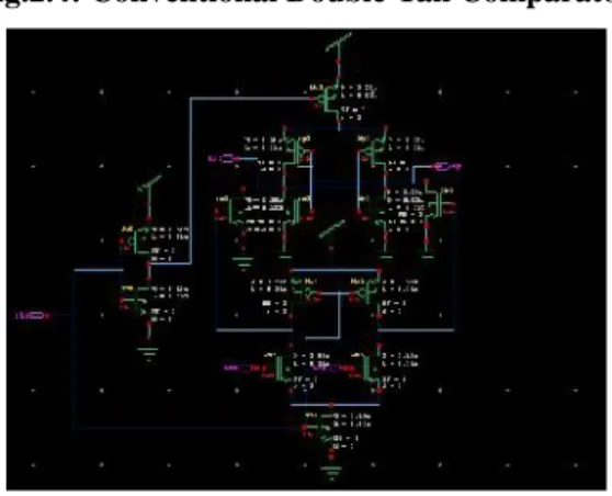
Fig.2.4: Conventional Double-Tail Comparator.
Fig2.5: Conventional Double-Tail Dynamic Comparator circuit design in tanner tool.
Fig.2.6: Lay out for fig.2.5
The operation of this comparator is as per the following. Amid reset stage (CLK = 0, Mtail1, and Mtail2 are off), transistors M3-M4 pre charge fn and fp hubs to VDD, which thusly causes transistors MR1 and MR2 to release the yield hubs to ground. Amid basic leadership stage (CLK = VDD, Mtail1 and Mtail2 turn on), M3-M4 kill and voltages at hubs fn and fp begin to drop with the rate characterized by IMtail1/Cfn(p) and on top of this, an info subordinate differential voltage ΔVfn(p) will develop. The moderate stage framed by MR1 and MR2 passes ΔVfn(p) to the cross coupled inverters and furthermore gives a decent protecting amongst info and yield, bringing about decreased estimation of kickback clamor Similar to the customary
includes two principle parts, t0 and t hook.
The deferral t0 speaks to the capacitive charging of the heap CLout (at the hook arrange yield hubs, Out n and Out p) until the principal n-channel transistor (M9/M10) turns on, after which the lock recovery begins; hence t0 is gotten After the primary n-channel transistor of the lock turns on (forM9), the comparing yield (e.g., Out n) will be released to the ground, driving front p-channel transistor (e.g., M8) to turn on, charging an-other yield (Outp) to the supply voltage (VDD). The recovery time (t hook) is accomplished.
1) The voltage distinction at the main stage yields (ΔVfn/fp) at time t0 profoundly affects lock introductory differential yield voltage (ΔV0) and subsequently on the hook delay. Consequently, expanding it would significantly diminish the postponement of the comparator.
2) In this comparator, both moderate stage transistors will be at last cut-off, (since fn and fp hubs both to the ground), thus they don't assume any part in enhancing the successful trans conductance of the hook. Moreover, amid reset stage, these hubs must be charged from ground to VDD, which implies control utilization. The accompanying segment portrays how the proposed comparator enhances the execution of the twofold tail comparator from the above perspectives.
III. PROPOSED DOUBLE-TAIL DYNAMIC
COM-PARATOR:
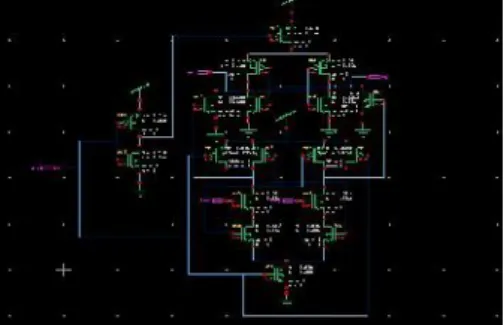
Fig. 4 shows the schematic chart of the hooked element twofold tail comparator. Because of the better execution of twofold tail engineering in low voltage applications, the proposed comparator is planned in view of the twofold tail structure. The principle thought of the locked comparator is to expand ΔVfn/fp so as to build the hookrecovery speed. For this reason, two control transistors (Mc1 and Mc2) have been added to the main stage in parallel to M3/M4 transistors yet in a cross coupled way.
Fig. 3.2: Latched comparator in Tanner Tool
Fig.3.3: Layout for fig.3.2
A. Operation of The Proposed Comparator Using Switching Transistor:
Fig.3.4: Proposed Double-Tail Comparator
The operation of the proposed comparator is as per the following in fig.3.4. Amid reset stage, clk = 0, tail transistors are set for maintaining a strategic distance from static power, M3 and M4 pulls both fn and fp hubs to Vdd, consequently transistor MC1 and MC2 are cut off. Middle of the road organize transistors, MR1 and MR2, reset both hook yields to ground. Amid basic leadership stage clk = Vdd, both the tail transistors are on, transistors M3 and M4 are kill. Toward the start of this stage, the control transistors are still off, since fn and fp are about Vdd.
Subsequently, fn and fp begin to drop with various rates as per the information volt-ages. Assume VINP > VINN, in this way fn drops quicker than fp, since M2 gives more present than M1.
For whatever length of time that fn keeps falling, the relating PMOS control transistor ,MC1 for this situation, begins to turn on, pulling fp hub back to the Vdd, so another control transistor (MC2) stays off, permitting fn to be released totally .at the end of the day, dissimilar to customary twofold tail dynamic comparator, in which ΔV fn/fp is only a component of info transistor transconductance and information voltage distinction, in the proposed structure when the comparator identifies that for example hub fn releases speedier, a PMOS transistor turns on, pulling the other hub fp back to the Vdd. In this manner when passing, the contrast amongst fn and fp (ΔV fn/fp) increments in an exponential way, prompting to the lessening of hook recovery time. Notwithstanding the adequacy of the proposed thought, one of the focuses which ought to be considered is that in this circuit, when one of the control transistors turns on, a current from Vdd is attracted to the ground through information and tail transistor, bringing about static power utilization. To defeat this issue, four NMOS switches are utilized beneath the info transistors, for example, Msw1, Msw2, Msw3 and Msw4.
B. Postpone Analysis:
The element comparator upgrades the speed of the twofold tail comparator by influencing two critical variables: in the first place, it expands the underlying yield voltage distinction (ΔV0) toward the start of the recovery (t = t0); and second, it improves the powerful transconductance of the lock.
1)Effect of Enhancing ΔV0: t0 is a period after which lock recovery begins. As such, t0 is thought to be the time it takes until the main NMOS transistor of the consecutive inverters turns on, with the goal that it will pull down one of the yields and recovery will start. The hook yield voltage contrast at time t0, (ΔV0) considerably affects the lock recovery time, with the end goal that greater ΔV0 brings about less recovery time.
This is because of the way that for bigger estimations of Vth/Vdd, the transconductance of the transistors diminishes, in this way the presence of an inward positive input in the design of the principal stage will prompt to the enhanced execution of the comparator.
3) Reducing the Energy per Comparison: In tradition al twofold tail topology, both fn and fp hubs release to the ground amid the basic leadership stage and every time amid the reset stage they ought to be pulled up back to the Vdd. In any case, in our proposed comparator, just a single of the said hubs (fn/fp) must be charged amid the reset stage. This is because of the way that amid the past basic leadership stage, in view of the status of control transistors, one of the hubs had not been released and hence less power is required.
C. Level Shifter using Double-Tail Comparator: to
Fig.3.5: Level shifter using double-tail comparator
Fig.3.6: Level shifter in tanner tool IV. Operation of the Level shifter circuit:
The Comparator has few applications. In which we designed Level shifter. Basically, scaling down of the technology and the trend of using small portable de- vices necessitates the much attention on low power design of CMOS circuits/systems and driven numerous research efforts to address various kinds of power reduction techniques. One of the most common techniques to reduce the leakage and dynamic power is to use multiple power supplies in a same system. In multi power domain systems different blocks operate with different power supplies. In
shifters are used among the blocks with different power supply domains. Mostly the level shifters are used as a constant Vdd supplier. Here we used voltage level shifters. We considered VL as low input voltage and VH as the high output voltage For any comparator circuit one input is the reference voltage and another input is the applied voltage. For level shifter application we considered only one input node. That means from the proposed double tail comparator INN is considered as reference input and INP is considered as applied input. INN is connected to INP with inverter. Here INN (VL) is only the input. The input voltage VL is given to the INN and output taken from Out n (VH). If VL =0.45v then VH=1.05V. Here VH is the applied Vdd. Always VL>VT. This simulation will be done in 45nm technology and implemented using Tanner 13 version. Applied frequency is 0.6GHz.
V. Analysis and Simulation Results:
Fig.5.1: simulation for fig 3.1
Fig.5.2: simulation for fig 3.4
Fig.5.3: simulation for fig 3.5
VI. Conclusion:
comparators were analyzed. Also, based on theoretical analyses, a new dynamic comparator with low-voltage low-power capability was proposed in order to improve the performance of the comparator. Post-layout simulation results in 0.045-μm
VII. Acknowledgement:
I am greatly indebted to my advisor Mr.G.S.S.Prasad for their valuable guidance, consistent encouragement and emphasis on the quality of the research contribution. Finally, and most importantly i would like to thank my teaching and non-teaching staff members for their support and unconditional love i have enjoyed throughout my life. References:
[1] Osaki, Yuji, et al. "A level shifter circuit design by using input/output voltage monitoring technique for ultra-low voltage digital CMOS LSIs." New Circuits and Systems Conference (NEWCAS), 2011 IEEE 9th International. IEEE, 2011.
[2] Babayan-Mashhadi, Samaneh, and Reza Lotfi. "Analysis and design of a low-voltage low-power double-tail comparator." IEEE transactions on very large scale integration (vlsi) systems 22.2 (2014): 343-352.
[3]Serneels, Bert, Michiel Steyaert, and Wim Dehaene. "A high speed, low voltage to high voltage level shifter in standard 1.2 V 0.13 μm CMOS."Analog Integrated Circuits and Signal Processing 55.1 (2008): 85-91.
[4] Ramanaiah, K. Venkata, and K. Padma Priya. "DESIGN OF LOW POWER HIGH SPEED LEVEL SHIFTER G. Srinivasulu."
[5] Tran, Canh Q., Hiroshi Kawaguchi, and Takayasu Sakurai. "Low-power high-speed level shifter design for block-level dynamic voltage scaling environment." Integrated Circuit Design and Technology, 2005. ICICDT 2005. 2005 International Conference on. IEEE, 2005.
[6] Dwivedi, Devesh, Suman Dwivedi, and Eswararao Potladhurthi. "Voltage up level shifter with improved performance and reduced power." Electrical & Computer Engineering (CCECE), 2012 25th IEEE Canadian Conference on. IEEE, 2012.
[7] Goll, Bernhard, and Horst Zimmermann. "A comparator with reduced delay time in 65-nm CMOS for supply voltages down to 0.65 V." IEEE Transactions on Circuits and Systems II: Express Briefs 56.11 (2009): 810-814.
[8]Schinkel, Daniel, et al. "A double-tail latch-type voltage sense amplifier with 18ps setup+ hold time." Solid-State Circuits Conference, 2007. ISSCC 2007. Digest of
Technical Papers. IEEE International. IEEE, 2007.
Mr.D.Anvesh received B.Tech degree in Electronics and communication Engineering from Pydah college of Engineering, Kakinada, Jawaharlal Nehru technological university, Kakinada, India, in 2014.Currently pursuing M.Tech in VLSI System Design from Kakinada Institute of Engineering and Technology, Kakinada, India. His area of interest is low power VLSI Design, System on chip and Network on chip, communication systems.
Mr.G.S.S.Prasad received the B.Tech degree in Electronics and communication Engineering from Acharya Nagarjuna university, Guntur, India, in 2001 and the M.Tech degree in VLSI System Design from Jawaharlal Nehru technological University,