Design of Multi-Hit Time-to-Digital Converter
Using Current Balanced Logic Delay Element
Pooja Saxena
Homi Bhabha National Institute, Anushakti Nagar, Mumbai 400094, India Email: [email protected]
K. Hari Prasad and V. B. Chandratre
Electronics Division, Bhabha Atomic Research Center, Trombay, Mumbai 400085, India Email: {khari, vbc}@barc.gov.in
Abstract—Multi-hit Time-to-Digital Converter (TDC) is an important functional unit in high energy physics (HEP) experiments to measure the accurate arrival time of multiple events. In this paper, a design and implementation of 4-channel Multi-hit TDC using Current Balanced Logic delay (CBL) element in 0.35µm CMOS technology is presented. The merit of CBL logic for tapped delay line provides lowest delay attainable for the delay element allowing better resolution in a given technology node compared to current starved inverter. The TDC is based on time stamping technique, where precise reference timing signals are generated from CBL based Tapped Delay Line (TDL). The TDC is operated in common stop mode, where timing of multiple consecutive hits are measured with respect to trigger. Each channel can measure the timing of four hits. The designed bin size is 150ps and dynamic range can be selected from 10µs to 40µs in steps of 10µs.
Index Terms—time-to-digital converter, delay lock loop, current balanced logic
I. INTRODUCTION
Precise measurement of arrival time of random events is needed in HEP experiments. To cater to this requirement, various techniques of TDCs [1]-[10] have been reported earlier. In India based Neutrino Observatory (INO) HEP experiment with 3.2 million detector channels, the TDC required is multi-channel, low cost, low power, with a bin size better than 200ps and dynamic range higher than 2.5µs. In addition to this, capability of measuring the arrival time of multiple events with high double-hit resolution (~5ns) is desirable to calculate the pulse width of the signal, so that timing corrections by using time over threshold can be implemented. In order to meet these requirements, we have designed Multi-hit TDC using 0.35µm CMOS process.
The design of TDC is based on time stamping using Tapped Delay Line (TDL) technique and counter [11]. This technique has been utilized in the development of multi-hit TDCs [12], [13] due to its salient features like small conversion time, multi-channel integration, and
Manuscript received July 4, 2015; revised May 1, 2016.
large dynamic range. However, the reported bin size (500ps) [13] of TDC depends on the smallest attainable delay from the delay element used to realize TDL. The aim of present design is to achieve the bin size of TDC better than 200ps, which is nearly comparable to the standard buffer delay in 0.35 µm CMOS process. Delay cells with small delays are required for safe designs. This issue has been addressed in [14] by using an area and power inefficient delay interpolation technique (array of delay lock loop) with current starved inverter based delay element. In other approach [15], high speed differential delay element with high static current and small delay regulation range has been used.
In this design, considering the power and area constraints, a fast voltage controlled delay element based on low noise Current Balanced Logic (CBL) [16] is designed. The salient features of this delay element are identical delays in the rising and falling edge transitions, high speed and area efficient as compared to current starved inverter. In addition, the static current in this delay element is less as compared to differential delay element. To provide the delay variation immunity across process and operating condition variations, a Delay Lock Loop (DLL) is designed [17], where single bias voltage controls both the rising and falling edge delays of CBL delay element in the design of multi-hit TDC.
The timing critical blocks in this TDC are DLL, TDL, register, and coarse count synchronizer. They have been designed using full custom analog design approach. The control logic, memory and readout interface are designed using digital design approach with automatic P & R tools. The paper is organized in the following sections: Section 2 discusses the design and implementation of TDC ASIC. Section 3 discusses the simulation results of time measurement.
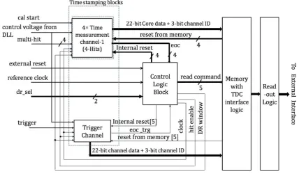
II. ARCHITECTURE OF MULTI-HIT TDCASIC
consecutive hits with respect to a reference clock (100MHz) within the dynamic range window. The duration of dynamic range window is selectable from 10µs to 40µs in steps of 10µs. The design aspects and implementation details of the time measurement channels have been discussed in detail in the sub-section A.
The logic control block is a key element in finding the hits that are associated with the trigger. This block opens a dynamic range window on an external or an internal reset. It also checks for the presence of trigger in the window. It issues a read command to the memory, to read the time measurement channels only if the trigger is
present in the window. If the trigger is not present, it generates an internal reset and reopens the window. Hence the scanning for hits that are associated with the trigger is being carried out with the help of this block.
On receiving the read command from the logic control block, the memory interface logic transfers the data from time measurement channels to an in-built memory. Further, the memory is interfaced with readout logic for TDC data transfer to external interface. The readout logic consists of Serial Peripheral Interface (SPI) and parallel interface. Any one of these two can be selected for external interface.
Figure 1. Block diagram of multi-hit TDC ASIC.
A. Time Stamping in Multi-Hit TDC
In the time stamping block, each measurement channel consists of a pre-processor, a 12-bit counter, TDL, coarse and fine registers, as shown in Fig. 2. The time stamping of multiple consecutive hits is carried out in two parts; coarse measurement using 12-bit counter and fine measurement using TDL. The TDL comprises of a cascaded chain of CBL delay elements.
It provides delayed replicas of reference clock with time interval of ‘Td’. This time interval defines the bin size of time stamping and depends on the smallest delay from CBL delay element.
The CBL delay element provides smallest delay of 135ps (at Vdd = 3.6V) and 150ps (at Vdd = 3.3V) in the used technology. For the smallest delay of 135ps, the number of delay elements in the delay line ‘N’ is equal to 74 as per equation (1), where Tref = 10ns. The control voltage provided by DLL assures that, the delay elements are immune to PVT variations.
Tref= N × Td (1)
Moreover, the double hit resolution is a crucial design aspect in time stamping for the consecutive hits. It defines the minimum measurable time interval between consecutive hits. Its specified value in INO experiment is 5ns. The TDL with single fine register cannot measure two consecutive hits occurring within its range (10ns), hence four fine registers are replicated, one for each hit. The TDL is dedicated for these registers and thus provides time stamping of consecutive hits with high double hit resolution. The pre-processor block separates these four hits (hit1 to hit4) comprised in the multi-hit signal for their time stamping.
(a)
(b)
Figure 2. TDC channel circuit (a) block diagram (b) timing diagram.
In coarse time measurement, the ‘hit’ is asynchronous to the operation of counter while sampling and latching its status. This may cause timing errors in measurement due to metastability and dead zone in coarse register. Moreover synchronization in coarse and fine counts is required to avoid an error of one clock period. A coarse count synchronizer shown in Fig. 3 based on the dual synchronization method [18] is designed to avoid the timing errors. Here ‘hit’ is synchronized to both the rising and falling edge of clock. A multiplexer is used to select the synchronized version ‘1’ or ‘2’ of hit as per its position within positive (‘a’) or negative (‘b’) half cycle of clock (Fig. 3(a)). Using sample 1 or 2, the ‘syn_hit’ is generated at falling edge of clock to sample and latch the counter when it is in idle state. It latches the state of counter (Nc) with one extra count, so one count is needed to be subtracted. Further, as fine counts are added to the coarse count, its accounted value is ‘Nc-2’ in arrival time calculation.
In fine time measurement, the first logic ‘1’ to logic ‘0’ transition in the 74-bit fine register gives the fine count ‘Nf’. A transition detector based on magnitude comparison between two consecutive bits of fine register detects the first logic ‘1’ to ‘0’ transition. The encoder converts the 74-bit count to 7-bit binary value to reduce the number of bits of fine time measurement. It has a feature to get disabled once detection of first logic ‘1’ to ‘0’ transition is completed. The 21-bit timing data
consisting of 12-bit coarse (NC), 7-bit fine count (Nf) and 2-bit hit ID corresponding to each hit, is stored in the register.
The arrival time of ‘hit’ is given by:
𝑇 = (𝑁𝑐− 2) × 𝑇𝑟𝑒𝑓+ 𝑁𝑓× 𝑇𝑑 (2)
(a)
(b)
The delay of CBL delay element is regulated by DLL across process and operating conditions. However, it is needed to be calibrated before calculation of arrival time of hits using (2). The accurate delay of the CBL delay element is found by measuring two known internal time intervals of 10 ns and 5 ns between ‘calstart’ and ‘calstop’. The time interval is generated by using reference clock and calibration is initiated by asserting ‘bincalibration’ (Fig. 2). The delay of CBL delay element ‘Td’ is given by difference of measured time interval using equation (3), where Nf1 and Nf2 are the counts of fine register corresponding to 10ns and 5ns respectively. The delay calibration is carried out periodically.
Td = (10 ns - 5 ns) / (Nf1- Nf2) (3)
III. SIMULATION RESULTS
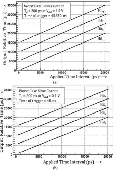
The design is verified using a mixed mode simulator. The post layout delay characteristic of CBL delay element is verified across five design process corners using Spectre simulator. Fig. 4(a) shows the delay versus control voltage characteristics of CBL delay element with identical rising and falling edge delays. Fig. 4(b) shows the delay characteristic across design process corners. On the worst case slow corner (WS), the best attainable delay from CBL delay element is 200ps. On typical corner, the delay of CBL delay element is150ps at Vdd = 3.3V and control voltage of 0.3V.
(a)
(b)
Figure 4. Delay vs. control voltage characteristic of CBL DE (a) typical (b) design process corners.
The performance of TDC channels is tested using Verilog test bench. The linearity of measured time characteristics is verified by applying linear sweep patterns of multi-hit in steps of 300ps with respect to trigger over 20ns range as shown in Fig. 5(a). Fig. 5(b) shows the plot between measured relative time of hits
versus applied time steps on typical (TYP) corner. This test is also performed across slow (WS) and fast (WP) design process corners for the bin size of Td = 200ps (control voltage = 0.1V) and Td = 150ps (control voltage =1.5V) respectively. The plots of measured characteristics are shown in Fig. 6(a, b).
(a)
(b)
Figure 5. (a) Applied test pattern to TDC channel (b) plot between relative time versus applied time
(a)
(b)
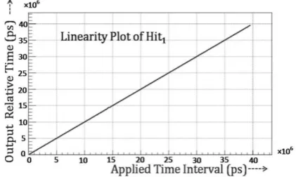
The performance over full dynamic range of 40 µs is verified by selecting values of 2-bit dr_sel as ‘11’. A linear sweep of multi-hits patterns with time steps of 223 ns with respect to trigger is applied to TDC channel. Fig. 7 shows the plot of relative time versus applied time step for hit1 on TYP corner.
Figure 7. Plot between relative time versus applied time for hit 1 over 40µs range
Table I shows the performance comparison with earlier reported TDCs based on the same technique. The significant improvement is achieved by using CBL delay element. It provides the bin size better than 200ps by using single DLL. This features a reduction in power consumption as compared to ADLL based TDCs. In addition to this, this delay element has identical delays in rising and falling edge transitions. This avoids the duty cycle correction circuit used in [19] to assure tapped delay matching in fine time measurement. Also, both edge delays are controlled by using single bias voltage. Further, in [1], [14], dual counter method is used in coarse time measurement; where opposite phases of clocks are applied to two counters with two coarse registers. At the time of occurrence of ‘hit’, at least one of the register is in stable state. This requires two coarse registers for each hit. In this design, the coarse count synchronizer uses only three flip-flops and multiplexer and requires single coarse counter and register. Hence, it further reduces the area and power consumption as compared to dual counter method.
TABLEI. PERFORMANCE COMPARISON
Parameters This work *** [1] [2] [12] [13] [14] [20]
Architecture of DLL
Single DLL with single loop
to control both edge delays
Single DLL
Array of
DLL Single DLL
PLL with ring oscillator
Array of
DLL Single DLL
N 74 16 100 16 16 140 128
Technology 0.35µm CMOS 1µm CMOS 1µm CMOS 1µm CMOS 0.3µm CMOS gate array 0.7µm CMOS 0.35µm CMOS
Bin Size 150ps 1.56ns 154ps 500ps 780ps 89.3ps 250ps
Dynamic range Selectable ( 10µs /20µs /30µs /40µs)
204.8ms --- 4.2ms 100µs 3.2µs ---
Double hit
resolution ~1ns Single hit Single hit 8ns --- Single hit Single hit Clock
frequency 100MHz 40MHz 65MHz 125MHz 80MHz 80MHz 32MHz
Architecture of Delay element
Current
Balanced DE CSI** CSI** CSI** CSI** CSI** CSI**
Power 50mW 10mW --- --- 500mW 800mW ---
Architecture of coarse count latching scheme Dual edge synchronizer Dual Counter Not mentioned Not
mentioned Not mentioned
Dual Counter
Not mentioned
Output code of Fine counter
Non-TH code corresponding to first ‘1’ to ‘0’
transition
*TH
code *TH code
Not
mentioned Not mentioned *TH code
Not mentioned
*TH code – thermometer code, ** CSI – current starved inverter, ***Comparison has been made in terms of architecture of basic blocks and design specification using Post Layout Simulation results (av- extracted)
IV. CONCLUSIONS
The 4-channel multi-hit TDC ASIC design using CBL delay element achieves bin size of 150ps over selectable dynamic range windows of durations from 10µs to 40µs in steps of 10µs. The design achieves a double hit resolution of better than 5ns. The design is tested for its linearity and robustness across design process corners. The issue of small delays in 0.35µm CMOS technology is successfully mitigated by using CBL logic.
REFERENCES
[1] C. Ljuslin, J. Christiansen, A. Marchioro, and O. Klingsheim, “An integrated 16-channel CMOS time-to-digital converter,” IEEE
Transaction on Nuclear Science, vol. 41, pp. 1104-1108, 1994.
[2] J. Christiansen, “An Integrated CMOS 0.15ns digital timing generator for TDC's and clock distribution system,” IEEE
Transaction on Nuclear Science, vol. 42, pp. 753-757, 1995.
[4] K. Koch, H. Hardel, R. Schulze, and E. Badura, “A new TAC based multi-channel front end electronics for TOF experiments with very high resolution,” IEEE Transaction on Nuclear Science, vol. 52, pp. 745-747, 2005.
[5] H. Flemming and H. Deppe, “Development of high resolution TDC ASIC at GSI,” IEEE Nuclear Science Symposium
Conference Record, vol. 1, pp. 322-325, 2007.
[6] Y. Kawakami, “1.2GaAs shift register IC for dead time less TDC,”
IEEE Transaction on Nuclear Science, vol. 36, pp. 512-516, 1989.
[7] Y. Arai and T. Ohsugi, “TMC-A CMOS time-to-digital converter VLSI for high energy physics,” IEEE Transaction on Nuclear
Science, vol. 36, pp. 528-531, 1989.
[8] K. H. Prasad, et al., “A four channel time-to-digital converter ASIC with in-built calibration and SPI interface,” Nuclear
Instruments and Methods in Physics Research, vol. 737, pp.
117-121, 2014.
[9] K. H. Prasad, et al., “FPGA based time-to-digital converter,” in
Proc. DAE Symposium on Nuclear Physics, 2011.
[10] K. H. Prasad, et al., “A CMOS standard cell based TDC,” in Proc.
International Conference on VLSI, 2013, pp. 87-93.
[11] J. Kalisz, Review of Time Interval Measurement Techniques with
Picoseconds Resolution, Institute of Physics Publishing, 2004.
[12] F. Bigongiari and R. Roncella, “A 250-ps time-resolution CMOS multihit time-to-digital converter for nuclear physics experiments,”
IEEE Transaction on Nuclear Science, vol. 46, pp. 73-77, 1999.
[13] Y. Arai, “A multi-hit time-to-digital converter VLSI for HEP experiments,” in Proc. Conference on Design Automation, Asia
and South Pacific, 2001, pp. 5-6.
[14] M. Mota and J. Christiansen, “A four channel self calibrating high resolution time-to-digital converter,” in Proc. IEEE International
Conference on Electronics, Circuits and Systems, 1998, pp.
409-412.
[15] K. Herve and C. Torki, “A 75ps rms time resolution Bi-CMOS time to digital converter optimized for high rate imaging detectors,”
Nuclear Instruments and Methods in Physics Research-A, vol. 481,
pp. 566–574, 2002.
[16] E. F. M. Albuquerque and M. M. Silva, “Current-balanced logic for mixed signal IC’s,” in Proc. IEEE International Symposium on
Circuit and System, 1999, pp. 274-277.
[17] P. Saxena, K. M. Sudheer, and V. B. Chandrate, “Design of novel current balanced voltage controlled delay element,” International
Journal of VSLI Design and Communication Systems, vol. 5, no. 3,
2014.
[18] J. P. Jansson, A. Mäntyniemi, and J. Kostamovaara, “Synchronization in a multilevel CMOS time-to-digital converter,”
IEEE Transactions on Circuits and Systems I: Regular Papers, vol.
56, pp. 1622–1634, 2009.
[19] G. Wu, D. Gao, T. Wei, C. Hu-Guo, and Y. Hu, “A high resolution multi-channel TDC for high energy physics and biomedical imaging applications,” in Proc. IEEE Conference on
Industrial Electronics and Applications, 2009, pp. 1133-1138.
[20] O. Bourrion and L. G. Martel, “An integrated CMOS time-to-digital converter for coincidence detection in a liquid Xenon PET prototype,” Nuclear Instruments and Methods in Physics Research
Section A, vol. 563, no. 1, pp. 100-103, 2006.
Ms. Pooja Saxena did her M.Tech. in VLSI design from Banasthali Vidyapeeth, Rajasthan, 2009. Currently, she is a research scholar in Homi Bhabha National Institute, Anushakti Nagar, Mumbai. She is working on design and development of CMOS time-to-digital converter.
Dr. V. B. Chandratre did his Ph.D. from Mumbai University. He did M.Sc. (Physics) from University of Poona and joined the 31st batch of BARC training school. His areas of expertise are nuclear instrumentation, Hybrid Microcircuits and ASICs. His fields of interest include nuclear pulse processing, data conversion, analysis, design of CMOS integrated circuits and TCAD. Currently he is involved in the development of ASICs and HMC design. He has made significant contributions to various DAE/ E&I programs.