Available Online at www.ijpret.com 64
INTERNATIONAL JOURNAL OF PURE AND
APPLIED RESEARCH IN ENGINEERING AND
TECHNOLOGY
A PATH FOR HORIZING YOUR INNOVATIVE WORK
DESIGN OF AREA-EFFICIENT BANDGAP REFERENCE IN 0.18µm CMOS
TECHNOLOGY
VRUSHALI G. NASRE,G. M. ASUTKAR
1. Department of Electronics & Telecommunication Engineering, P.C.E. Nagpur, INDIA. 2. Department of Electronics& Communication Engineering, P.I.E.T. Nagpur, INDIA.
Accepted Date: 27/02/2016; Published Date: 01/03/2016
\
Abstract: -A novel technique for a low supply voltage temperature-independent and area-efficient CMOS bandgap reference (BGR) is proposed in this paper. The low supply reference circuits is replaced by conventional bandgap reference circuit with the scaling of supply voltages, the threshold voltages don’t scale proportionally. The proposed circuit uses only three bipolar transistors to generate a reference voltage so that significant area reduction can be achieved. For design bipolar transistor device mismatch can be eliminated. The circuit produces an output voltage of about 650 mV, and simulated results show that the BGR is totally independent from temperature variation. The average current consumption is about 50 μA. The circuit was designed and simulated in 0.18μm CMOS technology in Tanner 13 tool.
Keywords:Bandgap Reference (BGR), Area efficient, Low supply.
Corresponding Author: MS. VRUSHALI G. NASRE
Access Online On:
www.ijpret.com
How to Cite This Article:
Available Online at www.ijpret.com 65
reference circuit with low supply voltage is expected for battery operated portable products. In CMOS technology, the conventional bandgap reference circuit usually uses the diodes to get the high precision bandgap voltage.
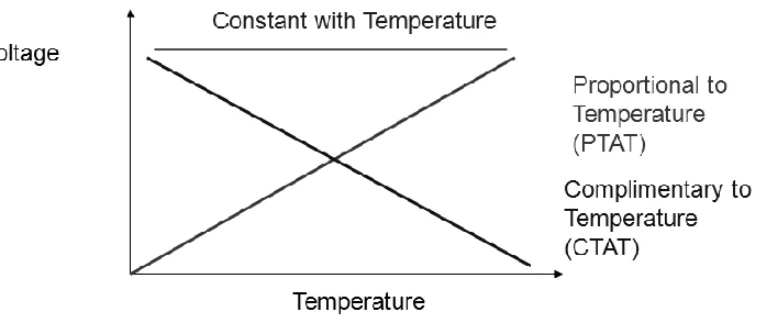
In bandgap reference, an output voltage with low sensitivity is obtained as the sum of a voltage that is proportional to absolute temperature (PTAT) and a voltage with negative temperature coefficient, which is complementary to absolute temperature denoted as (CTAT).
Figure 1. Block diagram of a bandgap voltage reference [1]
Available Online at www.ijpret.com 66
Figure 2. Concept of BGR
The term VT indicated in this figure1 is the thermal voltage described by (1), where K is the
Boltzmann Constant, q is the electron charge and T is the temperature [3].
T kT V q (1)
2. PRINCIPAL OF OPERATION
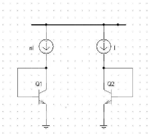
In Bandgap reference circuit reference voltages or currents that exhibit little dependence on temperature prove essential in many analog circuits. It is interesting to note that, if a reference is temperature-independent then it is usually process-independent as well because most process parameters vary with temperature. In order to generate a quantity that remains constant with temperature, we assume that if two quantities having opposite temperature coefficients (TCs) that are CTAT and PTAT added with proper weighting, the result displays a zero temperature coefficients. The forward voltage of a pn-junction diode and the base-emitter voltage of bipolar transistors exhibits a negative temperature coefficients i.e. CTAT. If two BJT bipolar junction transistors operate at unequal current densities, then the variation between their base-emitter voltages is directly proportional to the absolute temperature. As shown in Figure 3, if two identical transistors (I1 and I2 ) are biased at collector currents of nI0 and I0 and
their base currents are very small and can be neglected, then
1 2
BE BE BE
V V V
0 0
1 2
ln ln
BE T T
nI nI
V V V
I I
Available Online at www.ijpret.com 67
Figure 3: Generation of PTAT voltage
Thus, VBE the difference shows a positive temperature coefficient and given by
ln
BE
V k
n
T q
The proposed bandgap reference circuit is as shown in Figure 4 where M1 & M2 and M3 & M4
are identical which having ID1=ID2 so that voltage at X and Y are equal i.e. Vx=Vy.
3. SIMULATION RESULT
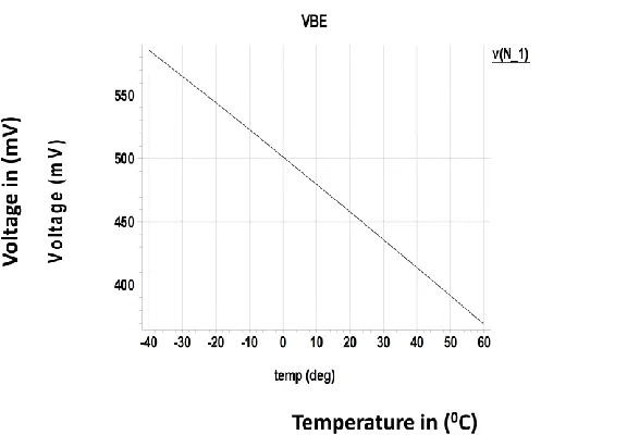
Simulation result of variation of VBE with temperature as shown in Figure 5. Where temperature is varies from -400C to 600C. The Figure 6. Shows the variation of ΔV
BE with respect
to temperature the maximum change in ΔVBE is not more than 1.05mV. The Variation of node X
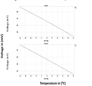
and Node Y potential with Temperature is as shown in Figure 7. The simulation result shows that there is identical variation in node potential with respect to temperature.
Available Online at www.ijpret.com 68
Figure 4. Proposed Bandgap Reference Voltage Circuit
Available Online at www.ijpret.com 69
Figure 6. Variation of ΔVBE with Temperature
Available Online at www.ijpret.com 70
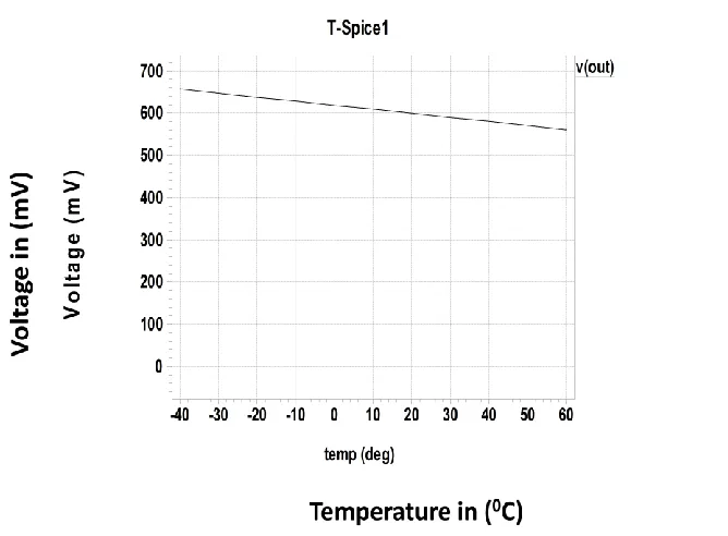
Figure 8. Variation of Output Reference voltage with Temperature
4. CONCLUSION
A low-voltage, low power three bipolar transistor bandgap reference circuit in the standard 0.18μm CMOS process is presented in this paper. The proposed bandgap reference circuit all MOS transistor are identical so that voltage at X and Y are equal. As a result, the low supply voltage 0.65V bandgap reference circuit with three bipolar transistors appears in this paper. The experimental results have proved that the bangap reference circuit is more stable with temperature variation. The average current consumption is about 50μA. The circuits are simulated in Tanner 13 tool with power supply of 1.8V.
5. REFERENCE
1. Christian Je´sus B. Fayomi, Gilson I. Wirth, Herve Facpong Achigui, Akira Matsuzawa “Sub 1 V CMOS bandgap reference design techniques: a survey” Analog Integrated Circuit Signal Processing 62:141–157 Springer-2010.
2. B. Razavi, Design of Analog CMOS Integrated Circuit. New York: McGraw-Hill, 2001.
![Figure 1. Block diagram of a bandgap voltage reference [1]](https://thumb-us.123doks.com/thumbv2/123dok_us/8709407.1740646/2.612.191.421.368.517/figure-block-diagram-bandgap-voltage-reference.webp)