Virtex 4 Field Programmable Gate Array Based 32 bit
FPM
Pardeep Sharma, Gurpreet Singh, Hartej Singh Saini
Assistant ProfessorShaheed Bhagat Singh State Technical Campus, Moga Road Ferozepur, Punjab (India)
E-mail: [email protected]
Abstract — FPGAs are increasingly being used in the high performance and scientific computing community to implement floating-point based hardware accelerators. We present FPGA floating-point multiplication. Such circuits can be extremely useful in the FPGA implementation of complex systems that benefit from the reprogramability and parallelism of the FPGA device but also require a general purpose multiplier unit. While previous work has considered circuits for low precision floating-point formats, we consider the implementation of 32-bit Single precision circuits that also provide rounding and exception handling. We introduce an algorithm for multiplication and analyze its performance on Virtex 4 having device (XC4VLX15-SF363) hardware module at speed grade -12.
Keywords - Floating point Multiplier, FPGAs, Xilinx and Virtex 4.
I.
I
NTRODUCTIONMany people consider floating-point arithmetic an esoteric subject. This is rather surprising because floating-point is ubiquitous in computer systems. Almost every language has a floating-point data type. Floating Point numbers represented in IEEE 754 format are used in most of the DSP Processors. Floating point arithmetic is useful in applications where a large dynamic range is required or in rapid prototyping applications where the required number range has not been thoroughly investigated. The floating Point Multiplier IP helps designers to perform floating point Multiplication on FPGA represented in IEEE 754 single precision floating point format. The single precision multiplier is divided into three main parts corresponding to the three parts of the single precision format [1]. The normalized floating point numbers have the form of
Z = (- ) * * (1.M) (1)
Where M = m22 2-1 + m21 2-2 + m20 2-3+…+ m1 2-22+ m0 2-23;
Bias = 127.
The first part of the floating point multiplier is sign which is determined by an exclusive OR function of the two input signs. The second part is the exponent which is calculated by adding the two input exponents. The third part is significant or mantissa which is determined by multiplying the two input significands each with a “1” concatenated to it. That “1” is the hidden bit. The main
applications of floating points today are in the field of medical imaging, biometrics, motion capture and audio applications, including broadcast, conferencing, musical instruments and professional audio.
II.
FPGA
(F
IELDP
ROGRAMMABLEG
ATEA
RRAY)
FPGA stands for Field Programmable Gate Array. It is a semiconductor device containing programmable logic components and programmable interconnects. The programmable logic components can be programmed to duplicate the functionality of basic logic gates such as AND, OR, XOR, NOT or more complex combinational functions such as decoders or simple mathematical functions [3] [8].
Fig.1. FPGA board
The development of these designs is made on regular FPGAs and then migrated into a fixed version that more resembles an ASIC. Complex programmable logic devices, or CPLDs, are another alternative.
III.
F
LOATINGP
OINTF
ORMATThe advantage of floating point format over fixed point format is the range of numbers that can be presented with the fixed number of bits. Floating point number is composed of three fields and can be of 16, 18, 32 and 64 bit. Figure shows the IEEE standard for floating point numbers [2].
Fig.2. Standard for floating point numbers
1 bit sign of signifies whether the number is positive or negative. „1‟ indicates negative number and „0‟ indicate positive number. 8 bit exponent provides the exponent range from E (min) =-126 to E (max) =127. 23 bit mantissa signifies the fractional part of a number the mantissa must not be confused with the significand. The leading „1‟ in the significant is made implicit [3].
A.
Conversion of Decimal to Floating numbers
Conversion of Decimal to Floating point 32 bit formats is explained in 1 & 2 example.
Example:
Step 1: Suppose a decimal number 129.85 is taken. Step 2: Convert it into binary number of 24 bits i.e.10000001.1101110000000000.
Step 3: Shift the radix point to the left such that there will be only one bit which is left of the radix point and this bit must be 1. This bit is known as hidden bit.
Step 4: Count the number of times radix points is shifted to the left say „x‟. The number which is formed after shifting of radix point is 1.00000011101110000000000. Here x=7.
Step 5: The number which is after the radix point is called mantissa which is of 23 bits and the whole number including hidden bit is called significand which is of 24 bits.
Step 6: The value „x‟ must be added to 127 to get the original exponent value which is 127 + „x‟. In this case exponent is 127 + 7 = 134 which is 10000110. Step 7: Number is +ve hence MSB of number is 0. Step 8: Now assemble result into 32 bit format in the form of sign, exponent and mantissa
01000011000000011101110000000000.
IV.
M
ULTIPLICATIONA
LGORITHM FORF
LOATINGP
OINTN
UMBERSAs stated in the introduction, normalized floating point numbers have the form of
Z = (- ) * * (1.M) (1)
Where M = m22 2-1 + m21 2-2 + m20 2-3+…+ m1 2-22+ m0 2-23;
Bias = 127.
To multiply two floating point numbers the following steps are taken [1] [6]:
Step 1: Multiplying the significand; i.e. (1.M1*1.M2) Step 2: Placing the decimal point in the result Step 3: Adding the exponents; i.e. (E1 + E2 – Bias) Step 4: Obtaining the sign; i.e. s1 xor s2 and put the result together
Step 5: Normalizing the result; i.e. obtaining 1 at the MSB of the results‟ significand shown in figure 3.
Fig.3. Normalization of sign, exponent and mantissa
Fig.4. Algorithm for floating point multiplication
B.
An example of floating point multiplier with
proposed algorithm
A: 0 10000111 10010101001110000101000 (32 bit) B: 0 10000110 10010010011010111000010 (32 bit) To multiply A and B
Step 1: Multiplying the significand (including hidden bit) 110010101001110000101000 (24 bit)*
110010010011010111000010 (24 bit)
=100111110011111100100111010001101001111001010 000 (48 bit)
Step 2: Placing the decimal point in the result
10.01111100111111001001110100011010011110010100 00
Step 3: Adding the exponents; i.e. (E1 + E2 – Bias) Adding of exponents =10000111 (E1) +10000110 (E2) The exponent representing the two numbers is already shifted/biased by the bias value (127) and is not the true exponent; i.e. EA = EA-true + bias and EB = EB-true + bias And EA + EB = EA-true + EB-true + 2 bias
So we should subtract the bias from the resultant exponent otherwise the bias will be added twice.
Exponent Result = 10000111 (E1) +10000110 (E2) – 01111111 (Bias 127) = 10001110
Eresult = 10001110
Step 4: Obtaining the sign; i.e. s1 xor s2 and put the result together
0 Xor 0 = 0, so the sign of the number is +ve 0 10001110
10.01111100111111001001110100011010011110010100 00
Step 5: Normalizing the result
Normalize the result so that there is a 1 just before the radix point (decimal point). Moving the radix point one place to the left increments the exponent by 1; moving one place to the right decrements the exponent by 1
Before Normalizing 0 10001110
10.01111100111111001001110100011010011110010100 00
After normalization 0 10001111
1.001111100111111001001110100011010011110010100 00 (including hidden bit)
Step 6: Rounding the result to the nearest number [3] [5] The mantissa bits are more than 23 bits (mantissa available bits); rounding is needed. If we applied the round to nearest rounding mode then the stored value is:
01000111100111110011111100100111(After rounding) Step 7: Checking for underflow/overflow occurrence
There are four main cases that the exponent is affected by normalization. It depends upon the Eresult that is calculated above [7] i.e.
Table 1 : Normalization effect on result‟s Exponent and Overflow/Underflow detection
Eresult Category Comments -125 ≤ Eresult <
0
Underflow Can‟t be compensated during normalization
Eresult = 0 Zero
May turn to normalized number
during normalization (by
adding 1 to it)
1 < Eresult < 254
Normalized number
May result in overflow during
Normalization 255 ≤ Eresult Overflow Can‟t be compensated
There are some special conditions while implementing floating point multiplier which needs to be handle these are explained in table.
The flow graph of overall algorithm for floating point multiplier including rounding is shown in figure 5.
V.
F
INALR
ESULTS/S
YNTHESISR
EPORTResults of Virtex 4 FPGA (XC4VLX15-SF363)Speed grade: -12
Table 2 Results/ Synthesis report
VI.
S
IMULATIONW
AVE FORM(
USINGM
ODELS
IM SIMULATOR)
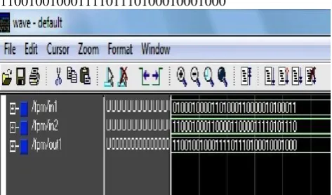
Case 1: When both the numbers are of same sign
1st input no. 405.22 =01000011110010101001110000101000 2nd input no. 201.21 =
01000011010010010011010111000010 Desired output no. 81534.31 = 01000111100111110011111100100111
Fig.6. Signals in Model Sim
Simulation result 81534.31 =
01000111100111110011111100100111
Fig.7. Simulation result for Floating point multiplier
Case 2: When both the numbers are of different sign
1st input No. 721.51 =01000100001101000110000010100011 2nd input No -902.12 =
11000100011000011000011110101110 Desired output no -650888.6 = 11001001000111101110100010001000
Fig.8. Signals in Model Sim
Simulation result -650888.6 =
11001001000111101110100010001000
Fig.9. Simulation result for Floating point multiplier
VII.
C
ONCLUSIONSThe floating point multiplier has been designed, optimized and implemented on Virtex 4 module. From the final results it is concluded that implementation of floating point multiplier on Virtex 4 (XC4VLX15-SF363) Speed Grade:-12causes small combinational delay i.e. 46.961 ns without offset and less number of slices (utilization of area) i.e. 663.
A
CKNOWLEDGMENTI would like to thanks the anonymous reviewers for their insightful comments.
R
EFERENCES[1] Al-Ashrafy M., Salem A. and Anis W., “An Efficient Implementation of Floating Point Multiplier”, 2011.
[2] Eldon A.J., Robertson C., “A Floating Point Format For Signal Processing”, pp. 717-720, 1982.
[4] Enriquez A.B., and JONES K.R., “Design of a Multi-Mode Pipelined Multiplier for Floating-point Applications”, pp. 77-81, 1991.
[5] Amaricai A., Vladutiu M., Udrescu M., Prodan L. and Boncalo O., “Floating Point Multiplication Rounding Schemes for Interval Arithmetic”, pp. 19-24, 2008.
[6] Louca L., Cook T.A. and Johnson W.H., “Implementation of IEEE Single Precision Floating Point Addition and Multiplication on FPGAs”, pp. 107-116, 1996.
[7] Awan M.A., Siddiqui M.R., “Resolving IEEE Floating-Point Error using Precision-Based Rounding Algorithm”, pp. 329-333, 2005.
[8] Fagin B., Renard C., “Field Programmable Gate Arrays and Floating Point Arithmetic”, pp. 365-367, Vol. 2, No. 3, 1994.
A
UTHOR’
SP
ROFILEMr. Pardeep Sharma
received M.Tech degree in Electronics and Communication Engineering from Sant Longowal Institute of Engineering & Technology in 2012 and received B.Tech degree in Electronics and Communication Engineering form Swami Vivekanand Institutes of Engineering & Technology, Banur in 2010. Currently, he is working as a Assistant Professor in Shaheed Bhagat Singh State Technical Campus, Ferozepur, Punjab. His area of interest is Digital Signal processing, VHDL, Wireless Mobile Communication Engineering, Digital Design and Analysis.
Mr. Gurpreet Singh
received M.Tech degree in Electronics and Communication Engineering degree from Jaypee University of Information and Technology, Solan in 2012 and received B.Tech degree from Lovely Institutes of Technology in Electronics and Communication Engineering from Lovely Institutes of Technology, Phagwara in 2010 with distinction. Currently, he is working as a Assistant Professor in Shaheed Bhagat Singh State Technical Campus, Ferozepur, Punjab. His area of interest is signal processing, MIMO, Wireless Mobile Communication Engineering, high speed digital communications and 4G Wireless Communications.