www.adv-radio-sci.net/11/231/2013/ doi:10.5194/ars-11-231-2013
© Author(s) 2013. CC Attribution 3.0 License.
Radio Science
Dead time optimization method for power converter
C. Deselaers1,*, U. Bergmann2, and F. Gronwald1
1Hamburg University of Technology, 21079 Hamburg, Germany 2Jungheinrich AG & Co. KG, 22844 Norderstedt, Germany *now at: DURAG GmbH, 22453 Hamburg, Germany Correspondence to: F. Gronwald ([email protected])
Abstract. This paper introduces a method for dead time op-timization in variable speed motor drive systems. The aim of this method is to reduce the conduction time of the free-wheeling diode to a minimum without generation of cross conduction. This results in lower losses, improved EMC, and less overshooting of the phase voltage. The principle of the method is to detect beginning cross currents without adding additional components in the half bridge like resistors or in-ductances. Only the wave shape of the phase voltage needs to be monitored during switching. This is illustrated by an application of the method to a real power converter.
1 Introduction
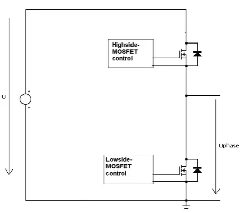
Power converter systems are used today in many applica-tions. In particular, in the context of battery supplied vehicles and similar areas the improvement of Electromagnetic Com-patibility (EMC) and the reduction of power losses become increasingly important. One approach to improve power con-verter systems in this respect is to reduce the dead time dur-ing switchdur-ing. To illustrate the concept of dead time, the fol-lowing Fig. 1 shows a typical half bridge, which is used in power converter systems:
In the operation of the half bridge the Highside- and Lowside-MOSFET are mutually switched. The dead time is here defined as the time delay between the falling edge of the control signal of one MOSFET and the rising edge of the control signal of the opposite MOSFET.
With the reduction of the dead time, the time in which the freewheeling diode conducts and the stored charge in this diode, which is responsible for the Reverse Recovery Effect (Polenov et al., 2009), can be reduced. This effect increases switching losses (Polenov et al., 2009; Reiter et al., 2010) and the snap off of the reverse current results in overvoltage and oscillation of the phase voltage (Semikron, 1998, p. 166).
Fig. 1. Principal circuit diagram of a half bridge.
In this context an optimal dead time can prevent the diode from conducting without generating a cross current in the half bridge.
plies to DC/DC-converters is described which changes the dead time until the duty-cycle command is minimized, cor-responding to maximized converter efficiency. This method uses the integrated voltage controller which doesn’t exist in that form in a power converter.
Another approach measures the voltage drop across the freewheeling diode (Mappus, 2003). The dead time is re-duced until this voltage drop no longer reaches the diodes forward voltage. But measuring this voltage drop is diffi-cult during current commutation because of the influence of induced voltages in the parasitic inductances (Rose et al., 2009).
In addition to these approaches there are several methods which use Zero Voltage Switching (ZVS), compare (Trescaes et al., 2004; Acker et al., 1995; Lau and Sanders, 1997). Most of these methods involve measuring the voltage drop across the switching transistor and the gate-source voltage which is compared to the threshold voltage. However, these approaches can only be used in conjunction with ZVS. In contrast to this, the method described in this paper is focused on a hard switching converter.
Beside the approaches above, there are further methods which apply to hard switching three phase power convert-ers. In Huselstein et al. (1993) an inductance is introduced in the half bridge. This allows detecting an occurring cross cur-rent from the change of voltage drop across this inductance: This change can be measured and then the dead time is re-duced until a cross current occurs. Here, the main problem is the inclusion of the inductance into the half bridge which can result in a worsening of the switching behavior. An ad-ditional method described in Rose et al. (2009) measures the threshold voltage of the MOSFETs involved. The beginning and the end of the current commutation is detected by means of a small inductance introduced in the half bridge. Since the complexity of this method is relatively high, a new de-signed gate driver is used to reduce the dead time according to this information. This can be disadvantageous because of-ten a simpler and more flexible method is desired which does not require a special Integrated Circuit (IC). Also an addi-tional inductance is needed and it can be assumed that the measurement of the threshold voltage has to be very exact to prevent cross conduction.
In this paper a method is presented which does not re-quire additional components in the half bridge. Only the wave shape of the phase voltage during switching has to be monitored. When a cross conduction occurs, this wave form changes, as it is also stated in (Yousefzadeh and Maksimovi´c, 2005) in view of DC/DC converter systems. These changes have been verified by means of simulation of a half-bridge and measurement in an existing power converter. This power converter is designed for low voltage applications, such that Power-MOSFETs can be used. A measuring circuit has been designed to detect this variation without the need of special or extremely fast components. The measured phase voltage
Fig. 2. Typical waveforms of the diode currentiDand the voltage
drop over the diodeuDof a blocking diode, as adapted from (Baliga,
2008). The supply voltage is denoted byU0.
is the basic for the proposed dead time optimization process which successively reduces the dead time until the changes in the wave shape of the phase voltage, that are due to the cross current, are detected.
The structure of the remainder of this paper is as follows: the origin of variation of the phase voltage, which is the ba-sis for the proposed method, is discussed in the following Sect. 2, where also the measuring circuit is introduced and important results of simulations and measurements are pre-sented. In Sect. 3 an actual implementation of the dead time optimization process is described and followed by a conclu-sion in Sect. 4.
2 Influence of the dead time on the switching behavior 2.1 Reverse Recovery Effect
When the MOSFET takes over the load current from the free-wheeling diode of the opposite MOSFET during switch-on, the Reverse Recovery Effect occurs when this diode blocks. The following illustration shows typical current and voltage waveforms during the blocking of the freewheeling diode.
First, the MOSFET starts to take over the load current from the diode during switch-on. Eventually, the MOSFET also has to carry a reverse current of the diode because the stored charge of the diode has to be degraded before it blocks. This results in higher losses in this MOSFET (Baliga, 2008, p. 245). Once the stored charge is degraded the freewheeling diode blocks and the reverse current quickly reduces to zero. This current change induces a voltage in the parasitic induc-tances of the half bridge (Semikron, 1998, p. 166). If the Re-verse Recovery Effect occurs at the transition low-high this voltage results in an overshoot of the phase voltage. The cor-responding additional contributionULσ to the phase voltage
ULσ =Lσ·
diD dt
R
(1)
Here, the internal inductances of the MOSFETs and of the junction lines are combined inLσ. The fast current change can also induce oscillations which have a negative impact on EMC (Rose et al., 2009; Semikron, 1998, p. 166).
2.2 Influence of reduced dead time on the Reverse Recovery Effect
The chargeQRstored in the freewheeling diode can be re-duced by decreasing the dead time because this leads to a de-creased conducting time of the freewheeling diode (Polenov et al., 2009). The peakIRMof the reverse current depends on this charge (Wang et al., 2004).
IRM= r
2·diD/dt·QR
1+S (2)
whereS is the softness factor of the diode. With a reduced peak, the slope of the reduction of the reverse current, i.e. the term diDdt
R, can be decreased as well (Baliga, 2008, p. 251). According to (1) this results in a lower voltage over-shoot. It is also mentioned that the losses in the MOSFET during switch-on are reduced due to the lower reverse cur-rent and faster switching (Polenov et al., 2009).
2.3 Influence of the cross current on the phase voltage In the same way as the decrease of the reverse current induces an overshoot of the phase voltage, the cross current can ini-tiate an overshoot of the phase voltage, too. Particularly, the reduction of the cross current is directed in a way such that the voltage induced in the parasitic inductances adds to the phase voltage.
To investigate this behavior, a half bridge was simulated with the main parasitic inductances and resistors included. An existing power converter served as basis for the simu-lations and also was used for subsequent measurements de-scribed below. Figure 3 shows the simulated wave shape of the phase voltage at a dead time where a cross current occurs. In Fig. 3, the second maximum is due to a decrease of the cross current, as has been confirmed by both simulation and measurement. The width of the peak that is associated to this second maximum depends on the magnitude of the cross current: a larger magnitude implies a larger width and vice versa. This effect can be used to detect the cross current, as described next.
2.4 Setup of the measurement circuit for detecting cross currents
The effect described in the previous paragraph also appears at the transition from the Highside- to the Lowside-MOSFET.
Fig. 3. Waveform of the phase voltage at a comparatively short dead
time where a cross current occurs.
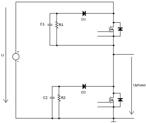
Fig. 4. Measurement circuits for detecting the over- and undershoot
of the phase voltage.
The sign of the induced voltage is such that it results in an ad-ditional decrease of the phase voltage. This leads to a second undershoot. As a consequence two measurement circuits are necessary: one for detecting the overshoots of the phase volt-age and one for detecting the undershoots at the other transi-tion. In Fig. 4 a possible design of these circuits is shown.
Fig. 5. Voltage across the capacitor for peak detection.
The voltage measured at the capacitor will be character-ized by a charging and discharging process and thus approx-imately have a triangular shape. Then a possibility is to mea-sure only the peak value of this voltage. An option to real-ize this is to use a capacitor with a diode put in series. This peak detecting capacitor then will be loaded until the maxi-mum voltage will be reached. To discharge this capacitor, a MOSFET put in parallel can be used. This MOSFET can be controlled by the microprocessor that realizes the dead time optimization.
It must be noted that the reference potential of the voltage across the capacitor C1 is given by the phase voltage while the microprocessor who measures this voltage has in most cases a ground reference potential. However, for converting the voltage across the capacitor C1, special ICs can be used, which are e.g. designed for current measurement with a re-sistor. The peak detection circuit can be set at the output of this IC such that the microprocessor can directly control the discharging MOSFET and measure the voltage over the peak detecting capacitor.
The circuit for detecting undervoltage behaves in the same way. In this case the measurement capacitor is charged when the voltage is below the ground potential plus the forward bias voltage of the diode D2. Here the usage of a peak detec-tion circuit in combinadetec-tion with a voltage transferring IC is also reasonable.
2.5 Influence of the dead time on the measured signal
To investigate the behavior of the measurement circuit of Fig. 4 it is integrated in the half bridge of an actual power converter, which can switch currents up to 400 A. With a successively reduced dead time, the ground referenced volt-age across the capacitor for peak detection, as described in the previous section, is measured.
Starting from a large dead time of 750 ns, the absolute value of this voltage decreases because of the reduced Re-verse Recovery Effect of the freewheeling diode which leads, according to Eq. (1), to a decreased overvoltage. It is then ob-served that at a dead time of approximately 350 ns the voltage starts to increase. At this dead time a beginning cross current
Fig. 6. Principle of the dead time optimization process. The variable
AD corresponds to the measured peak voltage.
was detected in several measurements and simulations. Also, beginning from this dead time, increasing losses were mea-sured due to the developing cross current.
At dead times around 350 ns the amplitude of the first overvoltage is strongly reduced in comparison to the larger dead time of 750 ns. But as the simulation result of Fig. 3 shows, the second overshoot becomes larger with increas-ing cross current. This change of wave shape can also be measured at the half bridge with decreasing dead time. Due to this wider second overshoot the measurement capacitor is stronger charged, which results in the increasing voltage drop. This rise can be detected by a dead time optimization method which is described in the following section.
3 Dead time optimization method
Fig. 7. Dead time optimization process. Curve 1: output of the DA-converter, proportional to dead time: an increase of the DA output voltage
corresponds to a decrease of the dead time. Curve 2: measured voltage over the peak detection capacitor C3.
temperature of the converter. This has to be analyzed for a given power converter system.
The PWM-controlling microprocessor has to measure the voltage over the peak detecting capacitors. These signals can directly be transmitted to the AD-converter. It is necessary that the microprocessor can influence the dead time, which is often the case. The dead time is now gradually decreased and after every step the actual voltage over a peak detecting capacitor has to be measured. As an initial condition of this process it is necessary that the capacitor is discharged via the MOSFET which is also controlled by this microprocessor. The discharge has to last until the capacitor C1 or C2 has adapted the new value, which usually takes about 200 µs to 400 µs. After this period, the peak detecting capacitor has to attain the peak voltage. This time depends on the IC used for the voltage transfer. For the cases considered, this time turned out to be about 200 µs.
In the actual process, first the measured peak voltage will decrease as it can be seen in Fig. 5. When the dead time ap-proaches the range where a cross current occurs an increase will be detectable. Figure 6 exemplifies this process.
This process has been integrated in the control of an actual half bridge. For exemplification a voltage was generated via a DA-converter which was chosen to be proportional to the dead time. In Fig. 7 a screenshot of the measured voltages illustrates this process.
First a reduction of the dead time leads to a decrease of the measured voltage. After every dead time reduction, which
here is about 50 ns, the peak detection capacitor is discharged until the measurement capacitor C1 has reached the new value. After the fourth step it is seen that the measured volt-age starts to increase. This is detected by the controller which then stops the dead time reduction. Since after the fourth step a small cross current exists, the controller increases the dead time about one step. As a result an optimal dead time is found to be about 380 ns.
3.2 Setting of the optimal dead time
Basically four switching transitions have to be distinguished, which are illustrated in Fig. 8.
When the load current is directed out of the half-bridge the Reverse Recovery Effect can be monitored at the transition low-high and in case that the load current runs in the half-bridge the Reverse Recovery Effect can be monitored at the transition high-low. For these two transitions a dead time op-timization is useful, as described above, to reduce losses and to improve EMC. The dead time at the other transitions can be chosen relatively high such that no cross current occurs. But it has to be mentioned that the described effect of second overshoot also appears at these transitions. Here it can also be useful to find the optimal, lowest dead time to increase the dynamic range of modulation.
tran-13 1
Fig. 8. Switching transitions in a half-bridge, indicated by curved arrows, as adapted from 2
(Huselstein et al., 1993). 3
4
When the load current is directed out of the half-bridge the Reverse Recovery Effect can be 5
monitored at the transition low-high and in case that the load current runs in the half-bridge 6
the Reverse Recovery Effect can be monitored at the transition high-low. For these two 7
transitions a dead time optimization is useful, as described above, to reduce losses and to 8
improve EMC. The dead time at the other transitions can be chosen relatively high such that 9
no cross current occurs. But it has to be mentioned that the described effect of second 10
overshoot also appears at these transitions. Here it can also be useful to find the optimal, 11
lowest dead time to increase the dynamic range of modulation. 12
To summarize, four different dead times have been determined. These are, depending on the 13
direction of the load current, two dead times for each switching transition. Therefore the dead 14
times have to be adjusted at each switching transition in the zero-crossing of the load current. 15
In many applications the controlling microprocessor measures or calculates the actual current 16
direction, such that this adjustment can easily be achieved. 17
18
4 Conclusion
19
The presented dead time optimization method provides a new alternative to existing 20
approaches. In contrast to the majority of these methods this approach does not need 21
additional components in the main current tracks of the half bridge, which would produce 22
additional losses. A suitable measurement circuit has been proposed to detect the changes in 23
Fig. 8. Switching transitions in a half-bridge, indicated by curved
arrows, as adapted from Huselstein et al. (1993).
sition in the zero-crossing of the load current. In many ap-plications the controlling microprocessor measures or calcu-lates the actual current direction, such that this adjustment can easily be achieved.
4 Conclusions
The presented dead time optimization method provides a new alternative to existing approaches. In contrast to the major-ity of these methods this approach does not need additional components in the main current tracks of the half bridge, which would produce additional losses. A suitable measure-ment circuit has been proposed to detect the changes in the wave shape of the phase voltage when a cross current occurs. This measured value is the basic variable of the dead time op-timization process. The proposed method also has been suc-cessfully tested in an actual half-bridge.
With this dead time reduction both the overshoot of the phase voltage and the switching losses are reduced. Also a considerable improvement in the EMC of the power con-verter has been observed.
So far this method has only been tested with MOSFETs but it should also be applicable to transistors such as IGBTs. Also the application in other contexts, such as the optimiza-tion of DC/DC-converters, is conceivable.
Acker, B., Sullivan, C. R., and Sanders, S. R.: “Synchronous recti-fication with adaptive timing control”, Proc. IEEE PESC, 1, 88– 95, 1995.
Huselstein J.-J., Gauthier, C., and Glaize, C.: Use of the MOSFET channel reverse conduction in an inverter for suppression of the integral diode recovery current, IEEE Power Electronics and Ap-plications, 2, 431–436, 1993.
Jayant Baliga, B.: Fundamentals of Power Semiconductor Devices, Springer Science+Business Media, LLC, Boston, MA, 2008. Lau, W. and Sanders, S. R.: An integrated controller for a high
fre-quency buck converter, Proc. IEEE PESC, 1, 246–254, 1997. Mappus, S.: Predictive Gate Drive Boosts DC/DC Power Converter
Efficiency, Texas Instruments, Appl. Rep. SLUA281, April 2003. Polenov, D., Reiter, T., Baburske, R., Probstle, H., and Lutz, J.: The Influence of Turn-Off Dead Time on the Reverse-Recovery Behaviour of Synchronous Rectifiers in Automotive DC/DC-Converters, IEEE EPE’09, 13th European Conference on Power Electronics and Applications, 8 pp., 2009.
Reiter, T., Polenov, D., Probstle, H., and Herzog, H.-G.: PWM Dead Time Optimization Method for Automotive Multiphase DC/DC Converters, IEEE Transaction on Power Electronics, 25, 1604– 1614, 2010.
Rose, M., Krupar, J., and G¨uldner, H.: Zero Body Diode Conduction Time in Variable Speed Drive Converter Systems, IEEE EPE’09, 13th European Conference on Power Electronics and Applica-tions, 10 pp., 2009.
Semikron Application Manual IGBT and MOSFET power modules, 1998.
Trescases, O., Ng, W. T., and Chen, S: Precision gate drive timing in a zero-voltage- switching dc-dc converter, Proceedings IEEE ISPSD’04, 16th International Symposium on Power Semicon-ductor Devices and ICs, 55–58, 2004.
Wang, Y., Zhang, Q., Ying, J., and Sun, C.: Prediction of PIN Diode Reverse Recovery, IEEE PESC, 4, 2956–2959, 2004.