DUTTA, SUMIT. Controls and Applications of the Dual Active Bridge DC to DC Converter for Solid State Transformer Applications and Integration of Multiple Renewable Energy Sources. (Under the direction of Subhashish Bhattacharya).
by Sumit Dutta
A dissertation submitted to the Graduate Faculty of North Carolina State University
in partial fulfillment of the requirements for the degree of
Doctor of Philosophy
Electrical Engineering
Raleigh, North Carolina 2014
APPROVED BY:
_______________________________ ______________________________
Subhashish Bhattacharya Iqbal Husain
Committee Chair
________________________________ ________________________________
BIOGRAPHY
ACKNOWLEDGMENTS
TABLE OF CONTENTS
LIST OF TABLES ... vii
LIST OF FIGURES ... viii
Chapter 1 Introduction ... 1
1.1. Research back ground ... 1
1.2. Motivation ... 3
1.3. Thesis outline ... 7
1.4. Research contributions ... 8
Chapter 2 Current Control of Dual Active Bridge Converter ... 10
2.1. Introduction ... 10
2.2. Motivation for implementing a fast current mode control ... 10
2.3. Peak current mode control ... 12
2.4. Predictive current mode control ... 15
2.4.1. Predictive Phase Shift Mode of Control ... 15
2.4.2. Predictive Half Cycle Phase Shift Mode of Control ... 16
2.4.3. Predictive Full Cycle Phase Shift Mode of Control ... 19
2.5. Duty cycle mode of control ... 23
2.6. Contribution of magnetizing current in the HF DAB transformer ... 28
2.6.1. Case 1: Entire Leakage is on primary side ... 30
2.6.2. Case 2: Entire Leakage is on secondary side ... 31
2.6.3. Case 3: Distributed Leakage ... 31
2.6.4. Case 4: Duty Cycle mode of control with Flux control ... 34
2.7. Predictive duty cycle mode of control ... 36
2.8. Half cycle mode of control ... 37
2.9. Full cycle duty cycle mode of control ... 38
2.10. Equal area mode of control ... 43
2.11. Power mode of predictive control ... 46
2.12. Experimental verification of predictive control ... 49
2.13. Conclusions ... 56
Chapter 3 Multi-terminal application for the Dual Active Bridge converter for multiple Renewable Energy Source integration ... 59
3.1. Introduction ... 59
3.2. Circulating current in a single limb core topology ... 60
3.3. Leakage inductance distribution and the impact on the circulating reactive power .... 62
3.4. Coaxial Winding transformer (CWT) based topology ... 63
3.5. Input current control in the CWT based topology ... 66
3.6. Series connected transformer based topology ... 67
3.7. Input current control in the series connected topology ... 69
3.8. A multi-limb transformer topology ... 71
3.10. Advantages of the MLC topology based on the copper usage ... 77
3.11. Magnetic core material requirement in MLC topology ... 80
3.12. Design of a MLC transformer based on the magnetic stage loss analysis ... 84
3.12.1. Core loss calculations ... 88
3.12.2 Copper loss calculations ... 92
3.13. Proximity effect in the windings ... 95
3.14. Power flow equations in the MLC topology ... 97
3.15. A small signal model for the MLC-based DAB converter for analyzing the parameter sensitivity ... 98
3.16.1. Transformer leakage inductor sensitivity analysis for open loop system ... 101
3.16.2. Design of a Compensator for improving the variation in stability due to variation in L 103 3.16.3. Evaluation of transfer function sensitivity coefficient: ... 105
3.16.4. Effect of wide variation in input voltage on the converter transfer function ... 107
3.16. Power smoothing algorithm using energy storage: ... 110
3.17. Experimental results: ... 112
3.18. Conclusions ... 116
Chapter 4 The solid state transformer application of the Dual Active Bridge converter ... 118
4.1. Introduction ... 118
4.2. Single phase SST cascaded topology ... 119
4.3. Voltage balance control of the SST ... 120
4.4. Inrush current limit at startup ... 126
4.5. Single phase SST topology with the MLC –DAB topology: ... 127
4.6. Experimental results of the single phase SST topology showing the soft start and the MLC-DAB integration: ... 130
4.7. The renewable energy hub concept ... 133
4.8. Energy management for the renewable energy hub ... 137
4.9. Parallel operation of Single phase SST ... 138
4.10. Controller design of the active front end of the SST ... 140
4.11. The single phase PLL ... 142
4.12. Local load management for the single phase SST ... 144
4.13. UPS operation of a single phase SST ... 148
4.14. Grid tied parallel operation ... 150
4.15. Black start operation of parallel connected SST in islanded mode ... 151
4.16. Critical load placement in SST topology: ... 157
4.17. Micro grid system stability ... 164
4.18. Black Start Sequence 4 ... 165
4.19. Conclusions ... 172
Conclusion ... 174
5.1. Summary of the main results ... 174
5.2. Further scope of future research: ... 177
LIST OF TABLES
Table 3.1: Current and power contributed by each source in the multi-active bridge topology
... 64
Table 3.2: Parameter definition and values required for optimum flux density calculation ... 87
Table 3.3: Peak flux and the number of turns obtained for the central and peripheral limb .. 88
Table 3.4: Steinmetz parameters for the ferrite material “F” (source: http://fmtt.com/Coreloss2009.pdf) ... 90
Table 3.5: Core volume data for the MLC transformer ... 90
Table 3.6: Core volume data for the SLC transformer ... 91
Table 3.7: Core loss data for the MLC and the SLC transformers ... 92
Table 3.8: Table showing the total resistance of the windings for the MLC transformer with 50 turns both on peripheral winding and 50 turns on the central winding ... 92
Table 3.9: R.M.S. current through the central and peripheral winding of the MLC-DAB at rated condition ... 94
Table 3.10: Table showing the winding resistance for the series connected core transformer ... 94
Table 3.11: Total loss for a 1 KW system in the MLC and the series connected case ... 94
Table 3.12: MLC-DAB converter parameters ... 100
Table 3.13: Leakage inductance dependence on the system stability ... 103
Table 3.14: Table showing the phase margin w.r.t change in L ... 104
Table 3.15: Variation in the phase margin of source to output transfer function with the variation in source voltage ... 108
Table 3.16: Variation in phase margin for the control to output transfer function ... 108
Table 4.1: Soft Start algorithm... 127
Table 4.2: Power modes of operation ... 138
LIST OF FIGURES
Figure 1.1: Solid State transformer topology ... 1
Figure 1.2: The SST topology with the DC micro-grid ... 2
Figure 1.3: The multi-active bridge topology with grid tied output (Solar panels from CA Solar) ... 5
Figure 1.4: Different configurations of a multi-port DC-DC topology with a high frequency accumulator stage as reported in [13]. ... 6
Figure 2.1: Block diagram of the DAB average current controller ... 11
Figure 2.2: Circuit diagram of the DAB converter ... 12
Figure 2.3: Peak Current Control (switching scheme) for the DAB ... 13
Figure 2.4: Controller for the peak current control. ... 14
Figure 2.5: Predictive phase shift control ... 17
Figure 2.6: Observer loop for the Phase shift Predictive Current Controller ... 17
Figure 2.7: Simulation result showing the effect of the observer ... 19
Figure 2.8: The Predictive Full Cycle mode of control implementation diagram ... 20
Figure 2.9: Stability loss due to inductor value mismatch ... 22
Figure 2.10: The Duty Cycle mode of control with the timing diagram ... 24
Figure 2.11: The Duty Cycle mode of control block diagram ... 25
Figure 2.12: Q vs Time Plot with traditional phase shift mode of control ... 26
Figure 2.13: Q vs Time Plot with duty cycle mode of control ... 27
Figure 2.14: Duty cycle control resetting the B-H curve of the Inductor ... 27
Figure 2.15: The T-model of the high frequency transformer with the distributed leakage between the primary and the secondary ... 29
Figure 2.16: Equivalent circuit of the High frequency DAB transformer ... 30
Figure 2.17: Controller for transformer flux DC level control in case of distributed leakage 33 Figure 2.18: Simulation results for the flux removal algorithm showing the magnetizing current averaged over one cycle. ... 33
Figure 2.19: Simulation results for the DC flux removal algorithm ... 34
Figure 2.20: Controller for complete DC flux removal ... 35
Figure 2.21: Simulation results for complete DC flux removal algorithm ... 35
Figure 2.22: Experimental results for DC flux removal algorithm ... 36
Figure 2.23: Controller diagram for the half cycle duty cycle mode of control ... 38
Figure 2.24: Transient response of the half cycle duty cycle mode of control ... 38
Figure 2.25: Timing diagram for the full cycle duty cycle mode of control using down counters ... 40
Figure 2.26: Timing diagram for the full cycle duty cycle mode of control using up-down counters ... 41
Figure 2.27: Simulation result for the full cycle duty cycle mode of control ... 42
Figure 2.28: Equal area mode of control ... 43
Figure 2.29: Transient response of the equal area mode of control ... 45
Figure 2.31: Power Balance in series input parallel output DAB stages ... 47
Figure 2.32: Power mode of predictive control ... 48
Figure 2.33: Controller block diagram for the power mode of predictive control ... 49
Figure 2.34: Transient test of the half cycle phase shift current mode control ... 50
Figure 2.35: Transient test of the half cycle phase shift current mode control showing the 𝐿𝑅 decay. ... 51
Figure 2.36: Transient test of the half cycle duty cycle current mode control. ... 52
Figure 2.37: Transient test of the half cycle duty cycle current mode control along with the changes in the duty cycles d1 and d2 ... 54
Figure 2.38: Controller diagram for the leakage inductance error compensation ... 55
Figure 2.39: Transient test of the leakage inductance error compensation... 56
Figure 3.1: The Multi-Active Bridge converter concept based on a single limb core topology ... 61
Figure 3.2: Circulating current due to voltage mismatch ... 61
Figure 3.3: Circulating current due to voltage mismatch in the primaries ... 62
Figure 3.4: Multi-terminal CWT based topology as a renewable energy accumulator ... 65
Figure 3.5: Input current control operation on the CWT based topology ... 67
Figure 3.6: The series connected topology ... 68
Figure 3.7: The Duty Cycle modulation to implement input current control ... 70
Figure 3.8: The MLC based topology ... 72
Figure 3.9: Electrical equivalent of the MLC topology ... 73
Figure 3.10: A three-limb transformer based topology ... 74
Figure 3.11: The natural gyrator principle ... 74
Figure 3.12: The bond graph model for the three-limb core transformer topology ... 74
Figure 3.13: Simplified bond graph model ... 75
Figure 3.14: Bond graph model with further simplifications ... 75
Figure 3.15: Electrical equivalent of the magnetic stage of the MLC topology ... 75
Figure 3.16: Electrical equivalent of the electrical stage of the MLC topology ... 76
Figure 3.17: Electrical equivalent of the three limb MLC topology ... 77
Figure 3.18: Flux path in a peripheral and the central winding ... 78
Figure 3.19: Plot of the gain factor w.r.t. the number of limbs ... 80
Figure 3.20: Flux plot for the MLC based topology ... 82
Figure 3.21: Flux plot for the SLC based topology ... 82
Figure 3.22: Three-limb MLC and SLC topology ... 84
Figure 3.23: B-H characteristic of the core material used for the construction of the MLC topology (source: http://www.mag-inc.com/products/ferrite-cores/f-material) ... 85
Figure 3.24: Core loss for the ferrite core material (F) (source: www.mag-inc.com/products/ferrite-cores/f-material) ... 85
Figure 3.25: Core dimensions for the used core 0P49925UC (source: www.mag-inc.com).. 89
Figure 3.26: The waveform showing the voltage and flux plot in the transformer core ... 90
Figure 3.28: Top view of the five limb core MLC topology ... 95
Figure 3.29: Electrical equivalent circuit of the MLC topology with the capacitors ... 96
Figure 3.30: Electrical equivalent circuit of the three limb core topology with two source and one load ... 97
Figure 3.31: Bode plot for the control to output transfer function 𝐺𝑣𝑑𝑠 showing the variation in phase margin with leakage inductance ... 101
Figure 3.32: Compensator designed to compensate for the variation in L ... 104
Figure 3.33: Variation of the phase margin and stability of the closed loop system with the compensator with the variation in the leakage inductance (L) of the transformer. ... 105
Figure 3.34: Sensitivity coefficient plot for the open loop system (green) and the closed loop system (blue) showing better attenuation of the sensitivity under closed loop operation .... 107
Figure 3.35: The plot of Gvg w.r.t. changes in the source voltage showing the stable phase margin ... 109
Figure 3.36: Magnitude and phase plot for the variation in control to output transfer function with the variation in input voltage ... 109
Figure 3.37: Power angle curve for the MLC topology ... 111
Figure 3.38: Control diagram for the energy management ... 111
Figure 3.39: Energy management algorithm from the power angle perspective ... 112
Figure 3.40: Lab setup for the MLC topology with the motor generator setup acting as a wave energy simulator ... 113
Figure 3.41: Experimental result showing the MLC regulating a DC bus with the wave energy and battery integrated ... 113
Figure 3.42: The five limb MLC transformer. ... 114
Figure 3.43: Terminal voltage waveforms for the five limb MLC transformer ... 114
Figure 3.44: Control diagram for the input current control operation on the 3 limb MLC topology ... 115
Figure 3.45: Experimental results for the three-limb MLC topology with input current control ... 116
Figure 4.1: Single phase SST topology with cascaded front end and DAB for the DC to DC stages ... 119
Figure 4.2: Vector Control of the active front end converter ... 120
Figure 4.3: DC voltage balance control for the front end ... 122
Figure 4.4: Power balance in the DAB stage ... 123
Figure 4.5: Simulation results with a voltage sag of 0.6 p.u. with the DC bus regulation intact ... 123
Figure 4.6 Input voltage sag of 0.3 p.u. with the DC bus collapse ... 124
Figure 4.7: A 0.3 p.u. voltage sag with modified DAB power balance control to maintain DC bus balance ... 124
Figure 4.8: Power angle curve for the DAB with different leakage inductors and operating at different phase shift angles to transfer the same power ... 125
Figure 4.9: Soft Start of the SST from the auxiliary power supply ... 127
Figure 4.11: The voltage sag simulated with a MLC topology based SST without using any
voltage bus balance control in the DC to DC stage as well as the front end stage ... 129
Figure 4.12: Experimental setup in the lab ... 130
Figure 4.13: Soft start algorithm (DC side waveforms) ... 131
Figure 4.14: Soft start algorithm (AC side waveforms) ... 131
Figure 4.15: Steady state operation of the MLC based SST topology ... 132
Figure 4.16: Experimental results showing the voltage sag compensation without the voltage bus balancing control (left). The right shows the startup pf the SST with the inrush current but without any voltage bus control ... 133
Figure 4.17: The renewable energy hub concept. ... 134
Figure 4.18: The single phase SST with the DC micro-grid concept. ... 134
Figure 4.19: MPPT operation on the renewable energy hub. ... 136
Figure 4.20: Input current control with different current references ... 136
Figure 4.21: PWM voltage waveform showing the duty cycle modulation in order to obtain the current control ... 137
Figure 4.22: REH with the mode switching operation using the grid as the energy buffer.. 138
Figure 4.23: The parallel connection of two single phase SST ... 139
Figure 4.24: The controller diagram for the d-axes control of the front end. The inner current loop (above) is shown followed by the outer voltage loop (below) ... 140
Figure 4.25: Controller diagram for the single phase d-q PLL with the all-pass filter for quadrature voltage vector generation ... 143
Figure 4.26: Power flow direction on the single phase SST ... 145
Figure 4.27: Local load management without the RES (left) and with power contribution from the RES (right) ... 146
Figure 4.28: Simulation results showing the change in polarity of Id with the RES switched on and off ... 147
Figure 4.29: Experimental results showing the current and voltage waveform of the front end with and without the RES turned on ... 147
Figure 4.30: The single phase SST as a UPS system with a critical load ... 148
Figure 4.31: Flow chart diagram of the black start system for the SST supplying a critical load ... 149
Figure 4.32: Experimental results of local load shedding during black start upon islanding from the AC grid. ... 150
Figure 4.33: Experimental results for the two SST connected in parallel with grid. SST 1 is in the regenerating mode while SST 2 is in the load mode taking power from the grid ... 151
Figure 4.34: Flow chart diagram for the black start operation with the slave SST front end acting as a rectifier under islanded mode ... 152
Figure 4.35: Experimental result of the black start of the parallel SST system with the slave SST front end working as a rectifier. ... 153
Figure 4.37: Experimental results of the black start operation under load shedding with the
critical load connected to SST 2 (slave DC stage) ... 155
Figure 4.38: Black start without the feed-forward term on the master SST voltage controller ... 155
Figure 4.39: Experimental results of the black start operation showing the PCC voltage regulated by the master ... 156
Figure 4.40: System diagram showing the critical load points ... 158
Figure 4.41: Slave SST showing the reconfigured winding arrangement. ... 159
Figure 4.42: Slave SST showing the reconfigured winding arrangement. ... 160
Figure 4.43: Black Start sequence (system diagram) ... 161
Figure 4.44: black start sequence flow chart diagram ... 162
Figure 4.45: Black Start transient showing the PCC voltage and the line current... 163
Figure 4.46: Experimental result showing the critical loads being kept undisturbed at the point of black start ... 163
Figure 4.47: Equivalent circuit diagram for the micro-grid with sequence 3 and sequence2. ... 164
Figure 4.48: Sequence 4 Black start circuit diagram ... 166
Figure 4.49: Flow chart diagram for the sequence 4 black start. ... 167
Figure 4.50: Experimental results for the black start sequence 4 ... 168
Figure 4.51: PCC voltage at the instant of black start (sequence 4) ... 169
Figure 4.52: DC stage and front end current wave form after islanding has occurred ... 170
Figure 4.53: Power flow path in case of 𝑃𝑅𝐸𝑆 >> 𝑃𝑙𝑜𝑎𝑑 ... 171
Chapter 1
Introduction
1.1. Research back ground
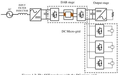
The recent years have seen the growing need of the renewable energy sources (RES) integrating to the conventional grid. With the development of Power Electronic converters along and the advancement of power semiconductor devices, RES can now be directly integrated to the existing grid by means of various power converter topologies. DC to DC converters provide the interface so that the RES can operate at maximum power point, and DC to AC inverters are used as an interface to the conventional 60 Hz grid. Amongst the several topologies that are available for the RES integration the solid state transformer (SST) topology is becoming widely popular [1], [2] concept. The SST is considered to be a replacement for the conventional 60 Hz transformer. It has an AC front end followed by an isolated DC to DC stage followed by inverter supplying a load or another grid (Fig. 1.1).
INPUT FILTER INDUCTOR AC
DAB stage Output stage
The SST unlike a conventional 60 Hz transformer is a multifunctional device. In addition to providing isolation it provides a DC bus to integrate the renewable energy sources to form a DC-micro grid [3], [4], [5].
INPUT FILTER INDUCTOR AC
RES
RES
RES
DC Micro-grid
DAB stage Output stage
Figure 1.2: The SST topology with the DC micro-grid
capability. It is capable of soft switching (ZVS turn on) that reduces the turn on switching losses. All these properties make the DAB a very suitable candidate for the SST application. The closed loop control and small signal transfer function of the converter has also been derived in [6], [8], [9]. The traditional control of the DAB converter is based on phase shift modulation where the leading bridge provides power to the lagging bridge. A dual loop control for the DAB has been proposed in [9]. Both the outer (voltage) and the inner (current) control loop are based in PI regulators with the assumption that the inner loop is faster than the outer loop by a factor of 10. This decouples the outer voltage and inner current loop but a bandwidth limit on the outer voltage control loop. To improve the outer voltage bandwidth, the inner current loop bandwidth needs to be improved which can be achieved by implementing a predictive current mode control. However in literature the predictive current mode control for the DAB has not been reported.
1.2. Motivation
Multi-Active Bridge Output stage
Renewable Energy Sources (Solar)
Grid
Battery/Storage
Figure 1.3: The multi-active bridge topology with grid tied output (Solar panels from CA Solar)
Renewable Source
Renewable Source
Grid
Load
Renewable Source
Grid
Load
Renewable Source
Renewable Source
Grid
High Frequency Accumulator
RES
1.3. Thesis outline
Chapter 2 discusses the predictive current mode control for the DAB converter. Based on the different sampling points of the switching cycle, there can be different predictive current controllers. The different current controllers have been discussed in details with simulation results. Experimental verification of the controller has also been shown with step change in the current response to show that as the reference changes, the controller is capable to track the change in one switching cycle. Since the controller is heavily dependent on the leakage inductance value, a compensation loop was also proposed to remove the error due to leakage inductance mismatch. The compensation algorithm has also been verified through experimental results.
Chapter 3 proposes the multi-terminal DAB converter for multiple renewable energy source integration. The problem of circulating reactive power has been addressed by implementing a multi-limb core transformer for the DAB (MLC-DAB) that acts as an energy accumulator. Power flow control was demonstrated with power smoothening using battery as an energy buffer. Input current control was also implemented and demonstrated with experimental verification showing the ability of the converter to do maximum power point tracking.
into the DC stage of the SST showing simpler control on the front end as well as the DC bus. A parallel MLC-SST test bed was developed and the system was islanded to form a micro-grid with two parallel SST. Power sharing was demonstrated under islanding condition with master-slave mode of control.
1.4. Research contributions
The following are the research contributions from the dissertation:
1. A duty cycle mode of control was developed for the Dual Active Bridge converter. 2. A phase shift based predictive current mode control was developed for the Dual Active
Bridge Converter.
3. A duty cycle based predictive current mode control was developed for the Dual Active Bridge Converter.
4. A stability analysis was performed to show the dependence of the phase shift mode predictive controller on the leakage inductance value and the stability limit have been reported.
5. A compensation algorithm was developed to compensate for the L-variation in the controller.
7. Equivalent circuit for the 3 – limb core and 5 – limb core based multi-limb transformer was developed using the gyrator principle.
8. A PWM based input current control algorithm was developed to separately control the source currents of different sources connected to the MLC-DAB converter.
9. An alternate DC - DC converter topology for the DC stage of the cascaded solid state transformer was proposed based on the multi-limb transformer topology (MLC-DAB based SST) and the advantages in the control applications were shown.
10.A renewable energy hub concept was proposed to integrate multiple renewable energy sources to the grid based on the MLC-DAB concept.
Chapter 2
Current Control of Dual Active Bridge Converter
2.1. Introduction
The Dual Active Bridge (DAB) converter (Fig. 2.2) has two H-Bridges (primary and secondary) that are switched at 50% duty cycle. Power flow is controlled from one bridge to another by phase shift modulation [6]. A duty cycle modulation for the DAB converter to increase the ZVS range under light load condition have been reported [14], [15], [48]. However no research has been done on implementing a fast predictive current mode control. Nor has there been any research on removing the DC bias in the high frequency transformer currents under load transients or steady state. The first section of this chapter provides the motivation of implementing a fast inner current loop along with the outer voltage loop. An analog based peak current controller is also proposed in the following section. Next the digital predictive current controller is proposed based on the phase shift approach. A duty cycle mode of control is proposed that is implemented to remove the DC bias in the transformer current. Finally a power based controller is proposed that allows parallel operation of the converters with power balancing. The proposed controllers are verified with simulation platform (MATLAB Simulink) and experimental results.
2.2. Motivation for implementing a fast current mode control
for the converter. For the Dual Active Bridge Converter, the inner current control is implemented by half cycle moving window averaging on the high frequency transformer current. The outer voltage loop gives the desired reference current. The inner current loop produces the phase shift to match the average current equal to the reference (Fig. 2.1). The inner loop is required to be faster than the outer loop by at least a factor of 10 [9]. The output of the inner current loop is the phase shift angle that controls the power flow from the primary to the secondary bridge. The average current (Fig. 2.1) can be obtained both from analog stage or digital stage (moving window averaging) based on the implementation requirement [1].
PI regulator
PI regulator ref
V
measured
V
ref
I
averaged
I
Mean Value
Figure 2.1: Block diagram of the DAB average current controller
can be made equal to the switching frequency i.e. 10 kHz allowing the maximum voltage control bandwidth to 1 kHz.
Voltage controller
Current Control
Phase Shift Current
reference
Primary Bridge Secondary Bridge
Power In Power out
HF Transformer
T1,D1
T2,D2 T3,D3
T4,D4 T2',D2' T4',D4' T1',D1' T3',D3'
Figure 2.2: Circuit diagram of the DAB converter
2.3. Peak current mode control
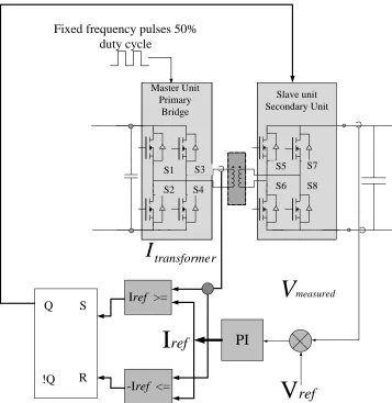
loop I0 is compared with the measured value Itransformer (Fig. 2.3 & Fig. 2.4) the switching
scheme for the control is shown in Fig. 2.3. The switching is realized using an S R flip flop. There is no phase shift as such unlike average mode of control. Power flow is hence controlled by the current reference generated by the voltage controller. Although the name of the controller is peak current mode control, it is really not the peak current that is being monitored. The reference current can be used to regulate the current at ωt = φ or the current at ωt = π
using different switching schemes. The switching scheme to regulate the current at ωt = φ has been discussed.
V
ref
PI
I
ref
Iref >=-Iref <= Q !Q S R S1 S2 S3 S4 S5 S6 S7 S8 Master Unit Primary Bridge Slave unit Secondary Unit
V
measured Fixed frequency pulses 50%duty cycle
r transforme
I
Figure 2.4: Controller for the peak current control.
The current I0 at ωt = φ that is set to follow the desired reference can be related to the input
voltage Vin and output voltage Vout as per (2.1).
𝐼0 = − 𝑉𝜔𝐿𝑖𝑛(𝑑𝜑 + 𝜋2 (1 − 𝑑)) , 𝑑 =𝑉𝑉𝑜𝑢𝑡
𝑖𝑛 , 𝜔 = 2𝜋𝐹𝑠𝑤𝑖𝑡𝑐ℎ𝑖𝑛𝑔 (2.1)
𝐹𝑠𝑤𝑖𝑡𝑐ℎ𝑖𝑛𝑔 is the switching frequency of the converter, L is the leakage inductance of the
for a perticular d the current I0 becomes fixed that drives the set and reset points on the SR flip
flop of the peak current control. This control is fast and takes place within one switching cycle of the of the converter. However the disadvantage is that continuous sampling is demanded and has to take place in analog domain. A digital implementation of this controller is difficut which provides the motivation for the predictive current mode of control where the sampling can take place once or twice within one cycle and the control implementation can be done based on those sampled values only.
2.4. Predictive current mode control
The predictive current mode control [10] works by predicting the next state control parameter (phase shift or duty cycle) based on the previous state values. The predictive control mode for the DAB converter based on the phase shift is discussed in the following section.
2.4.1.Predictive Phase Shift Mode of Control
The predictive phase shift control for the DAB is discussed in this section. The current is sampled once in every switching cycle and the phase shift angle is calculated and updated at the beginning of the next cycle. Based on the number of times the current is sampled in the cycle and update takes place and the calculations are done, the predictive phase shift mode of control can be classified as follows:
Both the methods have their own respective advantages and disadvantages from the control and parameter sensitivity point of view. The following sections discuss the two controllers in details.
2.4.2.Predictive Half Cycle Phase Shift Mode of Control
In this mode of control the current is sampled at θ = 0 and the current at ωt = π (or ωt =
φ) is the reference current and they are related as shown in Fig. 2.5 and Fig. 2.6. The required
phase shift angle is pre-calculated from the equations shown in (2.2a) or (2.2b) and updated at the beginning of each switching cycle. The disadvantage of this mode of control is the sampled point θ = 0 and the reference point ωt = π (or ωt = φ) are not the same (Fig. 2.5). Hence we might need an added loop that observes the reference point. This observer model can also serve as a control loop to reduce parameter sensitivity of the controller. A mismatch between the desired reference and the actual reference might occur of there is an error in the inductor value that has been fed to the controller. Under such circumstance the error will be carried over in the phase angle calculation without the controller knowing. Fig. 2.6 explains the idea behind the installation of the observer. In this particular case the predictive controller samples the current at ωt = 0 and the reference current is at ωt = φ. If the current is sampled at ωt = 0 and the current at ωt = φ is considered as the reference then the sampled current I0 is related to the
reference current Iref as follows in (2.2a)
𝐼𝑟𝑒𝑓= 𝐼𝜔𝑡=𝜑 = 𝐼0+𝑉𝑖𝑛+ 𝑉𝑜𝑢𝑡
I
transformerV
primaryV
primary
Sample point
Control point
Figure 2.5: Predictive phase shift control
Keeping the sampling point same if the current is referred at ωt = π the equation becomes as follows in (2.2b)
𝐼𝑟𝑒𝑓 = 𝐼𝜔𝑡=𝜋 = 𝐼0+
𝑉𝑖𝑛+ 𝑉𝑜𝑢𝑡
𝜔𝐿 𝜑 +
𝑉𝑖𝑛− 𝑉𝑜𝑢𝑡
𝜔𝐿 (𝜋 − 𝜑) (2.2𝑏) From either (2.2a) or (2.2b) the phase shift angle can be calculated in a deadbeat fashion. The phase angle updates within one cycle and does not depend on the previous state value. However since the sampled point is not observed, the predictive equation is heavily dependent on the accuracy of the measured leakage inductor value. In order to make the controller insensitive additional observer is introduced as shown in Fig. 2.6. The observer samples the current at the referring points on the switching cycle, at ωt = φ in the case of Fig. 2.6. Since this is the reference current, a proportion-integral control loop is implemented that adds an error phase angle to the predicted phase to compensate for the error (Fig. 2.6). Fig. 2.7 shows the simulation results with the observer in place. An error was intentionally inserted in the inductor value in the controller. Lactual was 100 μH while Lcontroller was 150 μH. The green in the figure
Figure 2.7: Simulation result showing the effect of the observer
2.4.3.Predictive Full Cycle Phase Shift Mode of Control
In this mode the sampled current and the referenced current occur at the same point. The controller samples the current at the mid-point of the half cycle i.e. at ωt = π/2 (Fig. 2.8). This sampling mode is adopted since sampling at the beginning (ωt = 0) or middle of the cycle (ωt
= π) means sampling at a switching instant. The current sensor may pick up the switching noise
the new value is loaded phase shift resistor and the effect takes place at the beginning of the next counter period when the counter starts counting up from zero. The next state phase shift angle φn+1 can be related to φn as per (2.3).
𝜑𝑛+1 = 𝜑𝑛+
(𝐼𝑛+1− 𝐼𝑛)𝜔𝐿
∆𝑉1− ∆𝑉2 , 𝑤ℎ𝑒𝑟𝑒 𝐼
𝑛+1 = 𝐼
𝑟𝑒𝑓 (2.3)
The principle advantage of this mode of control is that the sampled current and the reference current occur at the same point in the switching cycle. Hence an additional observer is not required. In case of inductance mismatch the system is convergent.
N
2 N 2 N 1. ADC Samples2. Interrupt for control calculation 3. New parameters loaded One Switching cycle n
n1n
I
I
n1n
n1D S P C O U N T E R D A B V O L T S A N D C U R R E N T S
It can be mathematically proven that in the event that there is an error in the leakage inductance measurement and if that error is within a particular bound, the actual current will converge to the reference current within several cycles. The proof is as follows:
𝑖𝑛+1 = 𝑖𝑛+∆𝑉2 𝜔𝐿 𝜋 4− ∆𝑉1 𝜔𝐿𝜑𝑛− ∆𝑉2
𝜔𝐿(𝜋 − 𝜑𝑛+1) + ∆𝑉1
𝜔𝐿𝜑𝑛+1+ ∆𝑉2
𝜔𝐿 ( 𝜋
4− 𝜑𝑛+1) (2.4) Where ∆𝑉1 = 𝑉𝑖𝑛+ 𝑉𝑜𝑢𝑡 and ∆𝑉2= 𝑉𝑖𝑛− 𝑉𝑜𝑢𝑡. Substituting 3 in 4 we get:
𝑖𝑛+1 = 𝐼𝑟𝑒𝑓(𝐿𝑑𝑠𝑝
𝐿𝑎𝑐𝑡) + 𝐼𝑛(1 − 𝐿𝑑𝑠𝑝
𝐿𝑎𝑐𝑡) = 𝐼𝑟𝑒𝑓( 𝐿
𝐿 + ∆𝐿) + 𝐼𝑛( ∆𝐿
𝐿 + ∆𝐿) (2.5)
Here 𝐿𝑑𝑠𝑝 = 𝐿 and 𝐿𝑎𝑐𝑡 = 𝐿 + ∆𝐿.
∴ 𝑖𝑛+2 = 𝐼𝑟𝑒𝑓( 𝐿
𝐿 + ∆𝐿) (1 + ∆𝐿
𝐿 + ∆𝐿) + 𝐼𝑛( ∆𝐿 𝐿 + ∆𝐿)
2
∴ 𝑖𝑛+3 = 𝐼𝑟𝑒𝑓( 𝐿
𝐿 + ∆𝐿) [1 + ∆𝐿 𝐿 + ∆𝐿+ { ∆𝐿 𝐿 + ∆𝐿} 2 ] + 𝐼𝑛( ∆𝐿 𝐿 + ∆𝐿) 3 ∴ lim 𝑘→∞𝑖𝑛+𝑘= 𝐼 = 𝐼𝑟𝑒𝑓( 𝐿
𝐿 + ∆𝐿) lim𝑘→∞[1 + ∆𝐿 𝐿 + ∆𝐿+ ⋯ { ∆𝐿 𝐿 + ∆𝐿} 𝑘−1 ] + 𝐼𝑛( ∆𝐿 𝐿 + ∆𝐿) 𝑘 (2.6) ∴ 𝐼 = 𝐼𝑟𝑒𝑓( 𝐿 𝐿 + ∆𝐿) 1
1 −𝐿 + ∆𝐿∆𝐿 = 𝐼𝑟𝑒𝑓 , 𝑠𝑖𝑛𝑐𝑒 lim𝑘→∞( ∆𝐿 𝐿 + ∆𝐿)
The above proof shows that if the measured value of the inductor Ldsp is offset from the actual
value of the inductance Lact by a margin of ΔL there is convergence in the geometric
progression (2.6) as long as ∆L ≤ L and the sampled current will converge to the reference current within several cycles. The simulation result in Fig. 2.9 shows the operation of the controller with gradually increasing ∆L. The Lact was 100 μH. In the figure when ∆L < L the
converter is stable and the sampled current tracks the reference current. But when ∆L = L occurs the current goes out of bound making the system unstable.
Figure 2.9: Stability loss due to inductor value mismatch
switches are duty cycle modulated. There are several advantages of that method of modulation. The normal proportional-integral based controller in duty cycle mode is discussed first followed by the predictive duty cycle based control.
2.5. Duty cycle mode of control
independent of each other. By changing one duty with respect to the other it is possible to apply positive volts seconds or negative volt seconds across the DAB inductor terminals and force a DC bias in the high frequency AC current. In other words if there is a DC bias already in the current, it is possible to remove it by selecting the duty cycles properly. The control loop shown in Fig. 2.11 has two inner current loops. In one loop the current sampled is ωt = 0 and in another loop it is ωt = π. From the timing diagram it is clear that the turn on period of S6 and S7 determines the value of 𝐼𝜋. Hence the loop containing 𝐼𝜋 produces the duty cycle d1 that
controls the opening and closing of S6 & S7. Similarly the loop with 𝐼0 controls the duty cycle for switches S5 and S8.
Since the duty cycle mode of control has two current loops (Fig. 2.11) the controller tries to regulate both the positive current and the negative current separately forcing the current to be AC through the DAB inductor. The advantage over normal 50% switching mode of control as shown in the simulation results of a DAB converter in Fig. 2.12.
ref V measuredV
PI
Outer Voltage Loop ref I I
Inner current loop 1d
0I
PI
Inner current loop -1 2d
PI
Figure 2.11: The Duty Cycle mode of control block diagram
The plot shows the integral of the high frequency inductor current over time (termed as “charge” or “Q”). When there is a DC bias in the current i.e. unequal volts-seconds has been
remove any residual magnetism in the core. This is not possible with the fixed 50% duty cycle mode of switching. With the duty cycle mode of switching this is possible by adding negative volts seconds across the inductor (Fig. 2.14) with the different combination of the duty cycles. However in-case there is an isolation transformer, this method fails to remove DC bias in the transformer core flux. Further discussion of this problem is presented in the following section.
DC VOLTAGE REMOVED
DC VOLTAGE
Time (sec)
Figure 2.13: Q vs Time Plot with duty cycle mode of control
B
H
DC bias in the transformer pushes the BH curve upwards Duty Cycle modulation can reset
the primary flux
POSITIVE BIAS
NEGATIVE BIAS
Residual magnetization
Residual magnetization
2.6. Contribution of magnetizing current in the HF DAB transformer
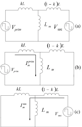
In the previous section the duty cycle mode of control was proposed which eliminates the DC bias in the high frequency load current. However the DC bias in the magnetizing current was not analyzed. Since dc bias in the magnetizing current and not the load current is responsible for saturating the high frequency DAB transformer it is important to analyze which bridge provides the magnetizing current to the transformer. This can be proved by analyzing the T-model of the high frequency transformer (Fig. 2.15). It can be assumed without any loss of generality that the primary side of the transformer has leakage kL and the secondary side ( 1-k)L. The magnetizing inductance is Lm. Superposition principle is used to calculate the
magnetizing current. Considering the primary voltage Vprim the magnetizing current
contributed by the primary bridge 𝐼𝑚𝑝𝑟𝑖𝑚is given by (2.7)
𝐼𝑚𝑝𝑟𝑖𝑚 = [ 𝑉𝑝𝑟𝑖𝑚 𝑘𝐿 + (1 − 𝑘)𝐿𝐿𝑚
(1 − 𝑘)𝐿 + 𝐿𝑚
] (1 − 𝑘)𝐿 [(1 − 𝑘)𝐿 + 𝐿𝑚]
= 𝑉𝑝𝑟𝑖𝑚(1 − 𝑘)𝐿
𝑘𝐿[(1 − 𝑘)𝐿 + 𝐿𝑚] + (1 − 𝑘)𝐿𝐿𝑚 (2.7)
(a)
(b)
(c)
Figure 2.15: The T-model of the high frequency transformer with the distributed leakage between the primary and the secondary
leakage inductance of the transformer and how each bridge contributes to the magnetizing flux and what can be the possible control strategy to maintain the flux to be AC.
Vout Vin
HF -transformer
S1,D1
S2,D2
S3,D3
S4,D4
S5,D5
S6,D6
S7,D7
S8,D8
(a) (b) (c)
Vin Vout Vin Vout Vin Vout
Figure 2.16: Equivalent circuit of the High frequency DAB transformer
2.6.1.Case 1: Entire Leakage is on primary side
The duty cycles cannot be adjusted to compensate for this as it might inject DC flux in the transformer. Thus this configuration of leakage inductance is not a good design to eliminate DC bias. Implementing such a transformer is possible with coaxial wound transformer (CWT) [18], [19], [20]. The CWT has the structural advantage that gives a control over the leakage inductance of the transformer. Hence by designing the CWT as such we can precisely place the leakage inductance of the transformer on the primary or on the secondary side.
2.6.2.Case 2: Entire Leakage is on secondary side
In the case that the entire leakage is on the secondary side (Fig. 2.16b) the load current is still a function of the duty cycles but the magnetizing current is not. The magnetizing flux is supplied by the primary bridge. Hence any unequal volt-seconds generated by the primary bridge due to non-idealities in switching [17] will lead to a DC flux in the transformer. The duty cycle modulation on the secondary will have no effect on the transformer flux. However, it can still be implemented to prevent saturation in the secondary side leakage inductance. The transformer bias can be eliminated by adding a positive or a negative bias in the primary switching. The inductor bias can be eliminated separately by the duty cycle modulation.
2.6.3.Case 3: Distributed Leakage
secondary bridge will be unable to remove the DC flux in the transformer core. To remove the DC flux an analog based controller is proposed (Fig. 2.17). Fig. 2.17 shows the controller for flux control in the transformer core. It is assumed the primary is fixed at 50 % duty-cycle. The secondary had a steady state duty cycle of 50 % onto which the controller adds ∆𝑑𝑠𝑒𝑐 . It is assumed that the primary and the secondary switching non-idealities add together to produce the unequal volt-seconds in the transformer core. The controller samples the primary current and the secondary current and takes a difference which gives the magnetizing current 𝐼𝑚 . Under ideal condition 𝐼𝑚 is AC or in other words the integral over one cycle (𝑄𝑐𝑦𝑐𝑙𝑒) will be zero. However if either the primary or the secondary bridge generates unequal volts-seconds
then DC offset will appear. The controller compensates by comparing the 𝑄𝑐ℎ𝑎𝑟𝑔𝑒to 0 by
+
-
AVG-
+ PI+ +
Flux control
50% ± 2% error
I
magQ
cycleQ
ref=0Figure 2.17: Controller for transformer flux DC level control in case of distributed leakage
Figure 2.19: Simulation results for the DC flux removal algorithm
2.6.4.Case 4: Duty Cycle mode of control with Flux control
+ +
+
-Flux control
50% ± 2 % error
Duty cycle based current mode control
V
primV
secI
primI
secI
mL
mL
1L
2d
1,d
2Figure 2.20: Controller for complete DC flux removal
DC bias in primary
Duty mode control in secondary
Flux control in primary
Figure 2.22: Experimental results for DC flux removal algorithm
Fig. 2.22 shows the experimental results for the proposed controller. The current sensors used for the purpose of measuring the high frequency DAB current are LEM sensors that output a current signal that is first converted to a voltage signal by a loading resistor and then sent to the ADC. By arranging the loading it is possible to isolate the magnetizing current and convert it into voltage and provide it to the ACD for DC bias measurement. Fig. 2.22 shows the experimental result of such an effort where the magnetizing current has been extracted from the primary and the secondary current difference and the DC bias has been calculated and compensation has been provided.
2.7. Predictive duty cycle mode of control
1) Half Cycle mode of control
2) Full cycle mode of control
3) Full Cycle equal area mode of control
2.8. Half cycle mode of control
In this mode of operation the sampling is done at two instances in the switching cycle, at
ωt = 0 and at ωt = π. The current sampled at ωt = 0 refers the current at ωt = π as the reference
and the current sampled at ωt = π refers the current sampled at ωt = 0 of the next cycle as the reference (Fig. 2.23). The equations driving the controller are given in (2.8a) and (2.8b).
𝐼𝑟𝑒𝑓𝜋 = 𝐼
0 + 𝑚1𝑑1𝑇𝑠+ 𝑚2(𝑇2𝑠− 𝑑1𝑇𝑠) (2.8a)
𝐼𝑟𝑒𝑓0 = 𝐼
𝜋 + 𝑚1𝑑2𝑇𝑠+ 𝑚2(𝑇2𝑠− 𝑑2𝑇𝑠) (2.8b)
Where 𝑚1 =𝑉𝑖𝑛+𝑉𝐿𝑜𝑢𝑡 , 𝑚2 =𝑉𝑖𝑛−𝑉𝐿𝑜𝑢𝑡. This control is a deadbeat control as the response takes
PI
Outer Voltage
Loop
Predictive equation (2.8b) -1
Predictive equation (2.8a)
Figure 2.23: Controller diagram for the half cycle duty cycle mode of control
Time (seconds)
Tr
an
sf
o
rm
er
cu
rr
en
t
(A
m
p
s)
Figure 2.24: Transient response of the half cycle duty cycle mode of control
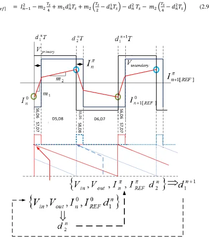
2.9. Full cycle duty cycle mode of control
Two different timing modes are discussed here. One with the sampling done at the beginning of the switching cycle (Fig 2.25) is using a down counter and another with sampling done at the middle of a half cycle using an down counter (Fig 2.26). The advantage of using the up-down counter is that the ADC can sample at the mid-point of the up count i.e. at count = N/2. This mode is preferred, since that the current sampled will be free of switching transients compared to the down counter used in Fig 2.25. Two up-down counters represented by the two triangles offset by 180◦ (black or counter 1 and dotted blue or counter 2) are required in this case as two currents are sampled, one in the positive half cycle and another in the negative
half cycle. The ADC samples when the counter is at 𝑁⁄2 at up-count of the black counter or counter 1. The sampled value is the current from the positive half cycle 𝐼𝑛1. Interrupt generated
at counter 1 = N does one set of the control calculations (2.9a). In the control calculations the
assumption is that the current in the next cycle i.e. 𝐼𝑛+1 1 will reach the desired reference value generated by the outer voltage loop. The computed value is 𝑑𝑛+11 and is loaded to the compare register of the counter 2. This generates the duty cycle for the counter 2 (the blue pulse in Fig. 2.26). Similar set of events take place with counter 2 one half-cycle earlier or later. The
negative current 𝐼𝑛−12 is sampled at up count of the counter 2. Interrupt is generated and the control calculations take place at counter 2 = N and 𝑑𝑛2 is calculated (2.9b) which is loaded on the compare register of counter 1 and generates the pulse shown in black (Fig. 2.26). The control calculations for the full cycle duty cycle mode are as follows
𝐼𝑛[𝑟𝑒𝑓]2 = 𝐼
𝑛−12 − 𝑚2𝑇4𝑠+ 𝑚1𝑑𝑛1𝑇𝑠+ 𝑚2(𝑇2𝑠− 𝑑𝑛1𝑇𝑠) − 𝑑𝑛2 𝑇𝑠− 𝑚2(𝑇4𝑠− 𝑑𝑛2𝑇𝑠) (2.9b)
S6
,D
6
S7
,D
7
D5,D8
S5
,D
5
S8
,D
8
D6,D7
S6
,D
6
S7
,D
7
One Counter cycle
D S P C O U N T E R D A B V O L T S A N D C U R R E N T S 3. New parameters loaded 1. ADC Samples 2. Interrupt 1. ADC Samples 2. Interrupt 3. New parameters loadedGate pulse for
Gate pulse for
Counter 2
Counter 1
Figure 2.26: Timing diagram for the full cycle duty cycle mode of control using up-down counters
2.27 shows the simulation result of the full cycle duty cycle mode of control. The transformer current is given a DC bias by switching off one of the devices in the primary of the DAB. The device is then turned on and it can be seen from the simulation result in Fig. 2.27 that the DC bias is removed within one switching cycle of the converter. Although this method is computationally simple, the current needs to be sampled twice in every switching cycle and with high frequency that may be difficult. Hence an alternate method is proposed where the current is sampled just once in the switching cycle and still the current is forced to be AC. The method is equal area method and is proposed in the following section.
2.10.Equal area mode of control
The equal area mode of control is an extension of the duty cycle mode of control. The idea is to sample the current at the start of the switching cycle and make it to follow a reference current that comes from the voltage PI controller. Considering the nth switching cycle and the (n+1)th cycle, we can get the following equation for the current:
𝑖𝑛+1 = 𝑖𝑛+𝑉𝑖𝑛+ 𝑉𝑜𝑢𝑡
𝐿 𝑑1𝑇𝑠+
𝑉𝑖𝑛− 𝑉𝑜𝑢𝑡
𝐿 (
𝑇𝑠
2 − 𝑑1𝑇𝑠) −
𝑉𝑖𝑛+ 𝑉𝑜𝑢𝑡 𝐿 𝑑2𝑇𝑠
−𝑉𝑖𝑛− 𝑉𝑜𝑢𝑡
𝐿 (
𝑇𝑠
2 − 𝑑2𝑇𝑠) (2.10)
s T d1 primary
V
ondaryV
sec 1A
2A
3A
4A
s sd
T
T
12
s T d2 ss
d
T
T
2
2
sampled
I
I
[ref]Assuming that in one cycle the corrective action is achieved and the above equation simplifies as shown in (2.11)
(𝐼𝑟𝑒𝑓− 𝐼𝑛) 𝐿
2𝑉𝑜𝑢𝑡𝑇𝑠 = 𝑑1− 𝑑2 (2.11)
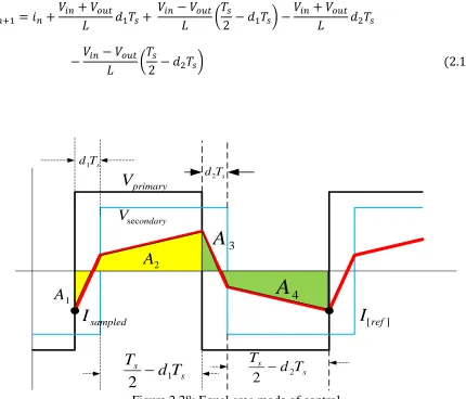
This is not enough to calculate the value of the duty cycles since there are two unknowns and one equation (2.11). This can be used to make the current through the transformer a perfect AC i.e. remove any DC offset in it. That can be done by equating the area under the curve of current in the positive half cycle (Fig. 2.28) (𝐴1+ 𝐴2) to that of the negative half cycle (𝐴3+ 𝐴4) i.e.
4 3 2
1
A
A
A
A
(2.12)Here (𝐴1 + 𝐴2) is a function of d1 and (𝐴3+ 𝐴4) is a function of d2. So from equations in
(2.11) & (2.12) we get the solutions for d1and d2 as in (2.13).
out
n ref s
out
out s out in s out s ref n out out s ref ref ref n n out s ref n out out s out in s out s ref out s ref n out out s n ref ref n n V T L I L I TV V T V V T V T L I L I TV V LT I L I L I I L I d V T L I L I TV V T V V T V LT I V T L I L I TV V LT I L I L I I L I d 4 4 4 2 4 2 4 2 2 2 2 2 2 2 2 2 2 2 2 2 2 2 2 2 2 2 1 (2.13)
controller is able to remove the dc bias in once cycle. The same exercise was done with a simple voltage based control and it is seen that it takes much more time for the controller to fully remove the DC bias in the current.
Figure 2.29: Transient response of the equal area mode of control
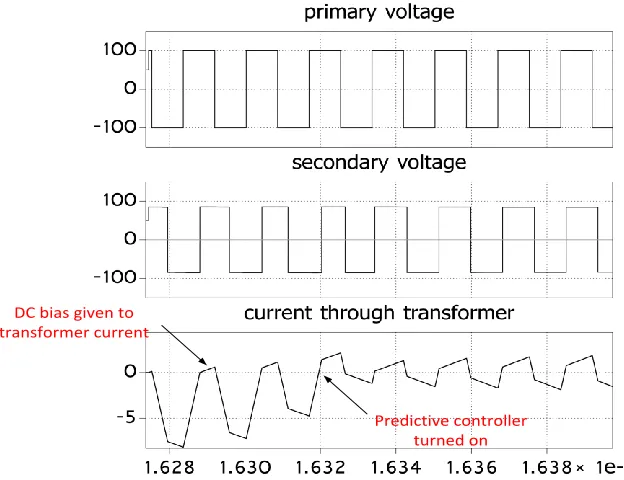
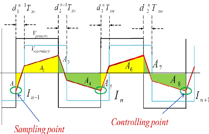
The Fig. 2.28 shows the equal area mode of control with instant update. However the controlling point may be two cycles down the line of the sampling point as shown in Fig. 2.29 with 𝐴1+ 𝐴2+ 𝐴5+ 𝐴6= 𝐴4+ 𝐴3+ 𝐴7+ 𝐴8
Predictive controller turned on DC bias given to
Figure 2.30: Equal area mode of control with control point two cycles down the line
2.11.Power mode of predictive control
So far the predictive controller regulates a particular current peak point within a cycle. But in case where there is power sharing required between parallel connected DAB converters (Fig. 2.31), this mode of control is not suffice. Here power balancing requirement is critical if the converters input stage is series connected to block higher DC bus voltage. The previously discussed methods will force the peak point currents to a referenced value. If the referenced value is at 𝜔𝑡 = 𝜑 where 𝜑 is the phase shift, then the expression of the current at that point is given as (2.14).
𝐼𝜑= 𝑉𝑖𝑛 𝜔𝐿[
𝑉𝑜𝑢𝑡 𝑉𝑖𝑛 𝜑 +
𝜋 2(1 −
𝑉𝑜𝑢𝑡
Figure 2.31: Power Balance in series input parallel output DAB stages
Considering multiple DAB connected with series input, parallel output mode with different leakage inductances (𝐿1,𝐿2…), the predictive controller with the current reference tracking,
will force the individual DAB to work at different phase shift angles (𝜑1, 𝜑2, … ) where according to (2.15),
𝜑1 𝐿1 ⁄ =𝜑2
𝐿2
⁄ = ⋯ (Assuming 𝑉𝑖𝑛 = 𝑉𝑜𝑢𝑡) (2.15)
But the power transfer equation for the DAB is given as (2.16).
𝑃𝑡𝑟𝑎𝑛𝑠𝑓𝑒𝑟𝑟𝑒𝑑 =𝑉𝑖𝑛𝑉𝑜𝑢𝑡
𝜔𝐿 𝜑 (1 − 𝜑
Hence for power balance in parallel connected DAB the relationship between the phase shift angle and the leakage inductance turns out as (2.17)
𝜑1 𝐿1 (1 −
𝜑1 𝐿1) =
𝜑2 𝐿2 (1 −
𝜑2
𝐿2) = ⋯ (2.17) Since the relationship mentioned in 2.15 ≠ 2.17 therefore the control modes discussed above is not suffice for power mode control. For that a different approach has to be taken that is somewhat similar to the area mode control discussed in the previous section. Fig. 2.33 shows the controller block diagram.
Figure 2.32: Power mode of predictive control sw
T
d
1 primaryV
ondary Vsec 1 A 2 A sw sw d TT 1 2 3
A
4A
swT
d
2 swsw d T
The current is sampled at 𝜔𝑡 = 0. An external voltage loop provides the power reference (Fig 2.33). With the generated Pref and the I0 from the sampled current the controller calculates the
required phase shift angle to produce the required power by calculating the area under the curve in the positive half cycle (yellow shaded portion in Fig. 2.32).
Figure 2.33: Controller block diagram for the power mode of predictive control
The phase shift angle calculated from the power mode control is given as (2.18).
𝜑 = 𝜋 − √𝜋√𝜋𝑉𝑖𝑛∆𝑉1𝑉− 2𝜔𝐿𝑃𝑟𝑒𝑓+ 2𝐼0𝜔𝐿𝑉𝑖𝑛
𝑖𝑛(∆𝑉1− ∆𝑉2) (2.18)
Where ∆𝑉1 = 𝑉𝑖𝑛+ 𝑉𝑜𝑢𝑡 and ∆𝑉2 = 𝑉𝑜𝑢𝑡− 𝑉𝑖𝑛 . This shows the relation of the phase angle with power is quadratic in nature as the way it should be from (2.16).
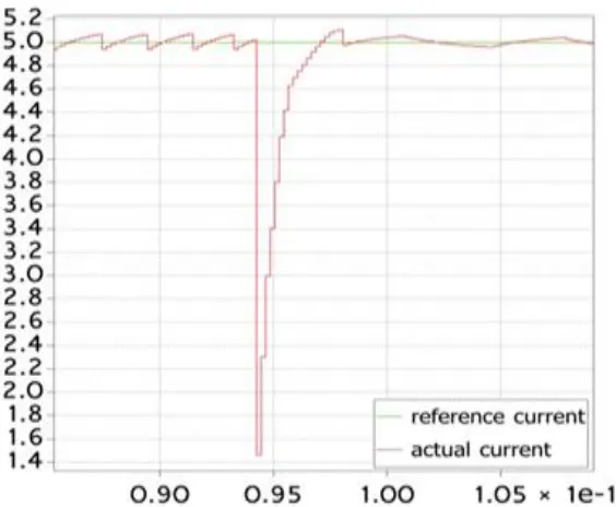
2.12.Experimental verification of predictive control
This section of the chapter presents the experimental verification of the predictive controller. In order to show the efficacy of the predictive controller, a step change in the current
PI
measured
V
ref
P
Predictivelaw
ref
V
o
reference was provided. If working properly, the controller will be able to track the change in one cycle (deadbeat control).
Figure 2.34: Transient test of the half cycle phase shift current mode control
Fig. 2.34 shows the step change in the current reference from the controller and the converter tracking the change in one cycle in deadbeat fashion. The control algorithm is mentioned in section 2.4.2 and equation (2.2a). The current is sampled at 𝜔𝑡 = 0 and referenced at 𝜔𝑡 = 𝜑. Based on the reference value the phase shift angle has been calculated. In the setup the
Figure 2.35: Transient test of the half cycle phase shift current mode control showing the 𝐿⁄𝑅 decay.
Fig. 2.35 shows the zoomed out view of the current response. This shows the 𝜏 = 𝐿 𝑅⁄ decay time for the current. In this present case the transformer shows a leakage resistance of 0.3 Ω.
would have manifested in the phase shift mode of control. The controller equations are similar to that in 2.8a and 2.8b and hence is not further derived.
Line
Current
Line
Voltage
Figure 2.36: Transient test of the half cycle duty cycle current mode control.
Fig. 2.36 shows the experimental result for the duty cycle mode of control. The important
red down counter corresponds to EPWM 1 while the blue counter corresponds to EPWM 3 phase shifted by π. ADC SOC is triggered every time EPWM 1 counter reaches the period
value and EPWM 3 counter reaches the period value. These SOC signals are OR-ed in the DSP and hence sampling take place two times in the cycle, once at 𝜔𝑡 = 0 and 𝜔𝑡 = 𝜋. The load mode registers in the EPWM modules are set to load the compare values in the registers immediately further reducing delay. Fig. 2.37 shows the duty cycle change with the step change in the current reference value from 1A to 2A. The predictive controller still requires an inductance information to operate optimally. However the leakage inductance of the transformer may change with time due to different causes. Hence a compensation algorithm was proposed in section 2.4.3 and simulation verification was shown in Fig. 2.7. However it requires further sampling at the point of referencing. In the experimental setup a simpler algorithm was implemented. Since in the first half cycle the current was sampled at 𝜔𝑡 = 0 and referenced at 𝜔𝑡 = 𝜑, it is first assumed that the current has reached the required reference at 𝜔𝑡 = 𝜑. With this assumption the current at 𝜔𝑡 = 𝜋 is calculated as per (2.19).
𝐼𝜋𝑐𝑎𝑙𝑐 = 𝐼𝑟𝑒𝑓+ ∆𝑉2 𝐿𝐷𝑆𝑃(
1
2− 𝑑1) 𝑇𝑠 (2.19)
Here ∆𝑉2 = 𝑉𝑜𝑢𝑡 − 𝑉𝑖𝑛 and 𝐿𝐷𝑆𝑃 (≠ 𝐿𝑎𝑐𝑡) is the erroneous inductance value input to the
controller and 𝑑1 is the duty cycle calculated from the predictive controller as per equations
(2.8a) and (2.8b). If 𝐿𝐷𝑆𝑃 = 𝐿𝑎𝑐𝑡 in that case 𝐼𝜋𝑐𝑎𝑙𝑐 = 𝐼𝜋𝑟𝑒𝑓. In order to compensate for the
replaces L in (2.8a) and (2.8b). Fig. 2.38 shows the controller block diagram for the compensation for the inductance error in the controller.
Duty
cycle d1
Duty
cycle d2
Line
Current
Figure 2.37: Transient test of the half cycle duty cycle current mode control along with the changes in the duty cycles d1 and d2
S6
,D
6
S7
,D
7
D5,D8
S5
,D
5
S8
,D
8
D6,D7
S6
,D
6
S7
,D
7
PI
SOC1
EPWM1 EPWM3
SOC3
Figure 2.39: Transient test of the leakage inductance error compensation
2.13.Conclusions
In this chapter the digital predictive current mode control have been applied to the DAB converter. The main results obtained in this chapter is summarized as follows:
A predictive phase shift controller was proposed for the dual active bridge
converter. The controller is of dead beat in nature and updates the control variable in one cycle.
The controller was shown to be sensitive of the leakage inductance value of the
A duty cycle mode of control was proposed for the Dual Active Bridge Converter.
The proposed control was shown to remove any DC bias in the transformer current by adjusting the duty cycles independently.
A predictive duty cycle mode of control was proposed. The proposed control was
shown to be dead beat in nature. In order to remove the DC bias in the transformer current an equal area criterion was imposed to calculate the duty cycles. The equal area criterion forces the area under the DAB transformer current waveform to zero to remove unwanted DC bias.
A power based predictive controller was proposed that predicts the phase shift angle
based on the required power transfer. The power based controller was shown to have second order response due to the quadratic nature of the power angle curve.
Experimental verification of the phase shift predictive controller was performed. A
step change in the current reference was provided and the controller was shown to
follow the reference in one cycle. However a 𝐿⁄𝑅 decay was shown to exist in the
current as per the transformer 𝐿⁄𝑅 time constant.
Experimental verification of the duty cycle mode of control was performed. With
a step change in the current reference, the controller was shown to respond within one switching cycle. Due to the asymmetric variation in the duty cycle, the current
An analysis was done to understand the contribution of the primary and the
Chapter 3
Multi-terminal application for the Dual Active Bridge
converter for multiple Renewable Energy Source integration
3.1. Introduction
![Figure 1.4: Different configurations of a multi-port DC-DC topology with a high frequency accumulator stage as reported in [13]](https://thumb-us.123doks.com/thumbv2/123dok_us/1307378.1163365/21.612.152.470.128.612/figure-different-configurations-multi-topology-frequency-accumulator-reported.webp)