Implementation of I
2
C Using ARM9
Controller
V.Lakshmi Bhavani1, K.R.K.Sastry2
PG Student [ESVD], Dept. of ECE, Gayatri Vidya Parishad College of Engineering (Autonomous), Visakhapatnam,
Andhra Pradesh, India1
Associate Professor, Dept. of ECE, Gayatri Vidya Parishad College of Engineering (Autonomous), Visakhapatnam,
Andhra Pradesh, India2
ABSTRACT:Data transmission with low power consumption, high speed and simple in design are the major concerns in embedded system. ARM9 is advanced version in microcontrollers with high speed, high performance and low power consumption. In this paper using LPC2929 board of ARM968E-S (from ARM9 family) controller for serial communication at high bit rate is implemented and analyzed. LPC2929 has peripheral interface devices such as I2C,
CAN, SPI, EEPROM, ADC/DAC, RS485 etc., The inter-IC (I2C) bus is a bidirectional bus provides communication
without data loss. Each device is recognized by a unique address and can function as a receiver-only device or as a transmitter in simplex operation. Work done for this journal involves I2C interface between ARM9 master to 24C02 (EEPROM) slave and read the stored data using RS485 protocol. The software for the system is implemented in Embedded ‘C’ using the Keil µ vision 4 cross compiler. Results are observed on Hyper Terminal.
KEYWORDS: I2C, EEPROM, ARM9,RS485.
I.INTRODUCTION
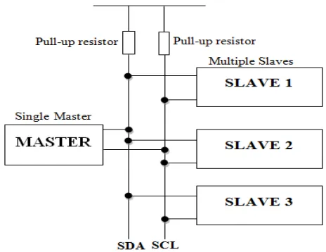
Embedded system design is mainly for making and managing communication between various bus interfaces and attaching multiple systems with different interfacing protocols to a main processor with high speed and low power consumption. ARM968E-S is a high performance; low power consumption microcontroller running at frequencies up to 125 MHz[4]. Embedded systems mainly uses serial communication to communicate with peripherals. I2C is a simple structured serial communication protocol, it gives excellent speed compared to other protocols. I2C uses only two wires for communication serial data line (SDA), serial clock line (SCL), so less number of wires required for connections and provides communication without data loss[2]. I2C bus supports for multiple masters and slaves. In this paper one master and two slaves are connected.
LPC2929 has on board EEPROM (24C02-EM/S(U2)) it is connected as one of the slave device for I2C protocol, with all
II.BLOCK DIAGRAM AND SPECIFICATIONS
Fig. 1 Block Diagram
I2C:
I2C bus stand for “Inter-integrated circuit” bus. I2C bus is a two-line (serial data line (SDA) and serial clock line (SCL))[2] serial bus developed in simple inexpensive communication, usually between ICs on the same printed circuit board. It connect low - speed devices like microcontrollers, EEPROMs, ADCs, DACs and other similar peripherals in embedded systems. I2C Devices are processors, EEPROMs, sensors, real-time clocks. It is used as a control interface, I2C devices can also have separate data interface. It was operated in 3 speeds. Those are,Slow (under 100 Kbps), Fast
(400 Kbps), High-speed (3.4 Mbps).
Fig. 2 I2C Block Diagram
The communication on an I2C bus is initiated by the bus master. The master generates clock signals (SCL) to permit data transfer. At this time, the device that is addressed is a slave. All communication starts with a START condition and ends with a STOP condition.
EEPROM
EEPROM stands for Electrically Erasable Programmable Read-Only Memory. The AT24C02 is an I2C compatible EEPROM provides 2048bits of serial electrically erasable and programmable read-only memory (EEPROM) organized as 256words of 8 bits each[3]. The device is optimized for use in many industrial and commercial applications where low-power and low-voltage operation are essential and it can save transmission time, increase the bus utilization time.
ARM9
ARM9 is a high performance, low power consumption microcontroller running at frequencies up to 125 MHz's consisting of 144 pins, in that 104 general-purpose I/O pins. It supports the Thumb instructions and widely accepted for applications which need high speed and high performance in MIPS per Watt[4]. Each I/O pins have four different functions. ARM9 has Harvard architecture. ARM9 has the separate instruction and data cache memory. It has separate instruction and data buses. It has a five-stage pipeline. It provides faster load and store due to more stages in pipeline. ARM9 gives higher performance than ARM7. The main advantages of ARM9 over ARM7 are
Decreased heat production and lower overheating risk.
Clock frequency improvements. Shifting from a three-stage pipeline to a five-stage one lets the clock speed be approximately doubled, on the same silicon fabrication process.
Cycle count improvements. Many unmodified ARM7 binaries were measured as taking about 30% fewer
cycles to execute on ARM9 cores. Key improvements include:
Faster loads and stores; many instructions now cost just one cycle. This is helped by both the modified Harvard architecture (reducing bus and cache contention) and the new pipeline stages.
Exposing pipeline interlocks, enabling compiler optimizations to reduce blockage between stages.
Additionally, some ARM9 cores incorporate "Enhanced DSP" instructions, such as a multiply-accumulate, to support more efficient implementations of digital signal processing algorithms.
ARM9 supports the Thumb instructions and this is available in ARM 9, T, E and J versions. ARM core-based MCUs based on ARM9 are widely accepted for applications needing high speed and performance in MIPS per Watt. The instructions use the byte, half-word (16-bit) and word (32-bit) for operations.
The main features of ARM are large register file R0 to R16, Load and Store Architecture data processing is only in register contents, Uniform and fixed length instructions, High code density, Mostly single-cycle execution, Speed is mostly 1Mhz to 1.25Ghz and In built circuit for debugging.
III.IMPLEMENTATION
Single Slave Mode:
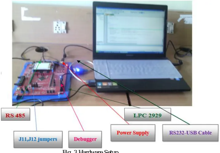
Fig. 3 Hardware Setup
Multiple Slave Mode:
AT24C02 is an external EEPROM, LPC 2929 board have two on board I2C protocols I2C0 and I2C1. Port1 10, 11, 12
and 13 pins are internally connected to this I2C0 and I2C1. In this I2C0, Pin11-SCL is used as Serial Clock line and pin 10-SDA Serial Data line.
AT24C02 consists of 8 pins. In that 5th and 6th pins are SDA and SCL; these two pins are connected to I2C0. 1st, 2nd and 3rd pins are connected to either ground or Vcc. These pins decide slave address of the AT24C02. Pins 4 and 8 are connected to ground and Vcc respectively. 7th pin is write protect, it is connected to ground.
Fig. 4 Hardware Setup for External EEPROM
IV.RESULTS & DISCUSSION
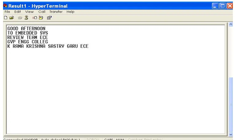
Fig. 5 Result on Hyper Terminal
The first four lines displayed on the HyperTerminal window are read from the Onboard EEPROM and the last line consists of the data read from the externally interfaced EEPROM. The size of the Onboard EEPROM is 2K bits which is divided into 16 pages, each capable of storing 16 bytes of data. The externally interfaced memory is also of 2K bits size, but it consists of 32 pages each capable of storing 8bytes of data.
V.CONCLUSION
In this thesis, the Inter integrated Circuit (I2C) bus protocol is implemented in Multi-slave mode using LPC2929 evaluation board which consists of ARM968E-S microcontrollers and several other on-board peripherals as well. The slaves used are two EEPROM chips, among which one is on-board and the other is externally interfaced. The results are displayed on HyperTerminal. By using this system, data is transferred with speed of 100kbit/s and distance up to 4000 feet (1200 meters).
REFERENCES
[1] Phaj Kumar Mehto, Pragya Mishara and Sonu Lal " Design and implementation for interfacing two integrated device using I2C bus", International journal of innovative research in computer and communication engineering, vol.2,issue 3, March 2013.