International Journal of Research (IJR) Vol-1, Issue-10 November 2014 ISSN 2348-6848
Effect of Current Feedback Operational
Amplifiers using BJT and CMOS
1
Ravi Khemchandani ;
2Ashish Nipane Singh &
3Hitesh Khanna
Research Scholar in Dronacharya College of Engineering Gurgaon
Abstract
The operational amplifier is an extremely efficient and versatile device. Its applications span the broad electronic industry filling requirements for signal conditioning, special transfer functions, analog instrumentation, analog computation, and special systems design. The analog assets of simplicity and precision characterize circuits utilizing operational amplifiers. The aim of the paper is to compare the CFOA implemented using BJT and the Current Feedback Operational Amplifier(CFOA) implemented using CMOS on the basis of Voltage Gain, Input and Output Impedance, Supply Voltage Rejection Ratio (SVRR), Common Mode Rejection Ratio (CMRR) and Slew Rate using Simulation Program with Integrated Circuit Emphasis (SPICE) simulation.
Keywords—
Inverting amplifier; Non inverting Amplifier; Differential amplifier; BJT; CMOS;CFOA
I. INTRODUCTION
An operational amplifier is a direct-coupled high-gain amplifier usually consisting of one or more differential amplifiers [1, 2]. The operational amplifier is a versatile device that can be used to amplify dc as well as ac input signals and was originally designed for performing mathematical operations. Originally, the term, “Operational Amplifier,” was used in
International Journal of Research (IJR) Vol-1, Issue-10 November 2014 ISSN 2348-6848
exponentially increasing current required for CMOS to achieve high speeds [4], bipolar are typically better suited for high bandwidth applications.
A. Basic Concept of Operational-Amplifier Configuration:
Generally there are three types of circuits: 1) Non-Inverting Amplifier: The input is applied only to the non- inverting input terminal and the inverting terminal is connected to ground. 2) Inverting Amplifier: The input is applied only to the inverting input terminal and the non-inverting terminal is connected to ground. 3) Differential Amplifier: The input is applied only to the inverting input terminal as well as the non-inverting terminal ground. The op-amp amplifies the difference between the two signals.
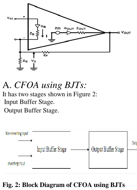
II. CURRENT FEEDBACK OPERATIONAL AMPLIFIER:
Basically operational amplifier can be made by using voltage feedback and current feedback. In this paper we stress on current feedback operational amplifier (CFOA) [3, 4] using bipolar junction transistor (BJT) and complementary Metal oxide semi
conductor (CMOS). CFOA is a type of Trans-Impedance Amplifier. In this model, it can be seen that the non inverting input is connected to the input of a unity gain, which usually takes the form of emitter follower circuit, and is modeled by GB and ZB [5, 6] (Figure 1).Since the non inverting input is the input of a buffer, it’s a high-impedance input. Now, because this buffer’s output connects to the inverting to input, CFOAs have lower inverting-input impedance,ZB. The current I flowing through the inverting input generates a voltage that is equal to current times the transimpedance Z This voltage is modeled by the output voltage source, Z(I). This voltage becomes the output voltage after passing through the output buffer, which is modeled by GOUT and ZOUT.
A.
CFOA using BJTs:
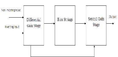
It has two stages shown in Figure 2: Input Buffer Stage.
Output Buffer Stage.
Fig. 2: Block Diagram of CFOA using BJTs
1)
Input Buffer Stage
: It is configured asInternational Journal of Research (IJR) Vol-1, Issue-10 November 2014 ISSN 2348-6848
Fig. 3: Operational Amplifier Using BJT
B.
CFOA using CMOS
It comprises of three subsections of circuit shown in Figure 4, namely
Differential Gain Stage. Bias Strings.
Second Gain Stage.
Fig. 4: Block Diagram of CFOA using CMOS
1)
Differential Gain Stage
: TransistorsQ1, Q2, Q3, and Q 4 form the first stage of the op amp the differential amplifier with differential to single ended transformation. Transistors Q1 and Q2 are standard N channel MOSFET (NMOS) transistors which form the basic input stage of the amplifier. The gate of Q1 is the inverting input and the gate of Q2 is the non-inverting input. A differential input signal applied across the two input terminals will be amplified according to the gain of the differential stage. The gain of the stage is simply the transconductance of Q2 times the total output resistance seen at the drain of Q2.The current mirror topology performs the differential
which constitutes the input of the second gain stage
2)
Second Gain Stage
: The second stage isa current sink load inverter. The purpose of the second gain stage, as the name implies, is to provide additional gain in the amplifier. Consisting of transistors Q5 and Q6, this stage takes the output from the drain of Q2 and amplifies it through Q5 which is in the standard common source configuration. Again, similar to the differential gain stage, this stage employs an active device, Q6, to serve as the load resistance for Q5. The gain of this stage is the transconductance of M5 times the effective load resistance comprised of the output resistances of Q5 and Q6.
3)
Bias String
: The biasing of theInternational Journal of Research (IJR) Vol-1, Issue-10 November 2014 ISSN 2348-6848
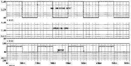
As we have applied input to the inverting terminal of op-amp so it is known as inverting amplifier. Fig. 6 shows its input and output waveform
Fig. 6: Simulation results of Inverting Amplifier using BJT
B.
Non- Inverting Amplifier Using
BJT
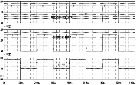
:As we have applied input to the inverting terminal of op-amp so it is known as non-inverting amplifier. Fig. 7 shows its input and
output waveforms.
Fig. 7: Simulation results of Non- Inverting Amplifier using BJT
C.
Differential Amplifier Using BJT:
As we have applied input to the non-inverting terminal and inverting terminal of op-amp using BJT so it is known as differential amplifier. Figure.8 shows its input and output waveforms
Fig. 8: Simulation results of Differential Amplifier using BJT
D.
Inverting Amplifier Using CMOS:
As we have applied input to the inverting terminal of op-amp using CMOS so it is known as inverting amplifier. Figure.9 shows its input and output waveforms
Figure 9: Simulation results of Inverting Amplifier using CMOS
E.
Non- Inverting Amplifier Using
CMOS:
International Journal of Research (IJR) Vol-1, Issue-10 November 2014 ISSN 2348-6848
Figure 10: Simulation results of Non-Inverting Amplifier using CMOS
F.
Differential
Amplifier
Using
CMOS:
As we have applied input to the non-inverting terminal and inverting terminal of op-amp using CMOS so it is known as differential amplifier. Figure.11 shows its input and output waveforms.
Figure 11: Simulation results of Differential Amplifier using CMOS
V. CONCLUSIONS:
In this paper we have implemented basic configurations of current feedback operational amplifier using CMOS and BJT. The voltage gain is found to be the same but the CMOS holds an advantage when it comes to Slew Rate, CMRR, Input Impedance and Power Dissipation whereas the Output Impedance comes out to be better for BJT. When we compare the basic
References
[1] Ramakant A. Gayakward, Op-Amps and Linear Integrated Circuits: Pearson Education .
[2] National Semiconductor, LM741 Operational Amplifier: August 2000
.
[3] S. Pennisi, High-performance CMOS current feedback operational amplifier, in Proc. IEEE Int. Symp. on Circ. and Syst. (ISCAS), II, Kobe, Japan, pp. 1573–1576 (2005)
[4] Heydari, P., Mohavavelu, R., “Design of Ultra High-Speed CMOS CML buffers and Latches,” Proceedings of the 200 Int’l
Symposium on Circuits and Systems, Vol. 2, May 2003
[5] Application note by Interstil, Converting from Voltage-Feedback to Current-Feedback Amplifiers.
\