FPGA-Based Configurable Systolic Architecture
for Window-Based Image Processing
C ´esar Torres-Huitzil
Computer Science Department, National Institute for Astrophysics, Optics and Electronics, P.O. Box 51 and 216, 72000 Puebla, Mexico Email:[email protected]
Miguel Arias-Estrada
Computer Science Department, National Institute for Astrophysics, Optics and Electronics, P.O. Box 51 and 216, 72000 Puebla, Mexico Email:[email protected]
Received 13 September 2003; Revised 21 May 2004
Image processing requires more computational power and data throughput than most conventional processors can provide. Designing specific hardware can improve execution time and achieve better performance per unit of silicon area. A field-programmable-gate-array- (FPGA-) based configurable systolic architecture specially tailored for real-time window-based image operations is presented in this paper. The architecture is based on a 2D systolic array of 7×7 configurable window processors. The architecture was implemented on an FPGA to execute algorithms with window sizes up to 7×7, but the design is scalable to cover larger window sizes if required. The architecture reaches a throughput of 3.16 GOPs at a 60 MHz clock frequency and a processing time of 8.35 milliseconds for 7×7 generic window-based operators on 512×512 gray-level images. The architecture compares favorably with other architectures in terms of performance and hardware utilization. Theoretical and experimental results are presented to demonstrate the architecture effectiveness.
Keywords and phrases:FPGA, configurable system, real time, window-based image processing, systolic array.
1. INTRODUCTION
Designing a hardware processor core for data-intensive im-age processing is a fundamental step in developing
mod-ern machine vision systems that can efficiently implement
computer vision related tasks. The wide interest in data-intensive or window-based image processing is due to the fact that more complex algorithms use the low-level
re-sults as primitives to pursue higher-level goals [1].
How-ever, building such systems remains difficult because of three
main reasons [2]. First, most computer vision applications
are computational intensive tasks difficult to overcome using
conventional processors. The sequential nature of conven-tional processors and the huge amount of redundant data in-volved in an image slow down the performance of vision sys-tems. Second, heterogeneity of computations in the process-ing performed through an application limits the paralleliza-tion. A mismatch, therefore, exists between the complex-ity of the required operations and the processing power of-fered by processors. Third, several vision applications require systems with real-time performance. A real-time system is one that must interact with its environment under
response-time constraints [3,4]. Real-time image processing systems
interact with their environment, and thus they must produce outputs that are not only numerically correct, but which also meet timing constraints necessary for these interactions.
On the other hand, advances in computer technology have made the building of machine vision systems a tractable problem, resulting in a widespread use of these systems in ap-plications such as robotics, multimedia, virtual reality, indus-trial inspection, medical engineering, and autonomous nav-igation. However, processing power, physical size, and power consumption constraints restrict further the extent to which these applications are solved under the perspective of systems
on a chip [5].
Previously, there have been several architectures pro-posed in the literature to implement window-based image
processing algorithms [6,7,8]. However, almost all of them
focus on the performance of a single image processing al-gorithm, usually 2D image convolution, without considering implementation aspects such as flexibility, silicon area, and power consumption.
In this paper, we propose an improved 2D systolic ar-chitecture as an alternative solution to implement window-based image processing algorithms on a single chip with
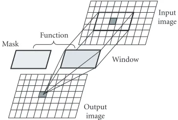
Input image
Window Function
Mask
Output image
Figure1: Conceptual view of a window-based operator.
organized as follows. Section 2describes the basis of
win-dow-based image processing. The systolic architecture orga-nization and the processing element structure are described in Section 3.Section 4presents the complexity and perfor-mance issues of the architectural model. Experimental results and the performance analysis of the FPGA implementation
are presented inSection 5. Discussion and comparison are
given inSection 6. Finally, conclusions and further work are
presented inSection 7.
2. WINDOW-BASED IMAGE PROCESSING
The first stages of computer vision require a large number of repetitive neighbor or window-based operations over a mas-sive amount of image data. The window-based operation do-main is restricted to a small neighbor of image data centered on a reference pixel. A conceptual view of window-based
op-erators is depicted inFigure 1. A window-based operation is
performed when a window, area ofw×wpixels, is extracted
from the input image and it is transformed according to a window mask or kernel and mathematical functions to
pro-duce an output result [1,9,10]. The window mask is the
same size as the image window and their values are usually constants through the entire image processing. The values used in the window mask depend on the specific type of fea-tures to be detected or recognized. Usually a single output data is produced by each window operation and it is stored in the same position as the central pixel of the window.
Window-based operations can be formalized
mathemat-ically as follows. LetIbe theM×Ninput image,Ythe output
image, andWaw×wwindow mask. A 2D window operation
can be defined as
Yrc=F
fwi j,Ir+i,c+j
∀(i,j)∈w×w,∀(r,c)∈M×N, (1)
wherewi jrepresents a coefficient from the window maskW,
Ir+i,c+jrepresents a pixel from aw×wwindow around the
(r,c) pixel in the input image, f defines a scalar function,
andadefines the local reduction function.
Window-based operators are characterized because the same scalar function is applied on a pixel by pixel way to each individual pixel of one or more input images to pro-duce a partial result. Common scalar functions include rela-tional operations, arithmetic operations, logical operations,
Table1: Complexity of image convolution expressed in terms of arithmetic operations.
Elemental operations Number of executions
Multiplication w2×M×N
Addition (w2−1)×M×N
Load/store (2×w2+ 1)×M×N
and possibly look-up tables. The local reduction function re-duces the window of intermediate results, computed by the scalar function, to a single output result. Some common local reduction functions employed are accumulation, maximum, and absolute value. Scalar and local reduction functions form the image algebra to construct window-based image
appli-cations [9,11]. Thus, to design flexible hardware
architec-tures for window-based image processing, the architecture instruction set must support these functions.
2.1. Computational requirements
Window-based image operations in computer vision are computationally expensive tasks. The window-based oper-ation complexity can be expressed in terms of the
elemen-tary arithmetic operations required to process an image [8].
In particular, analyzing image convolution, the total num-ber of operations required to perform this task, excluding ad-dress generation and other control actions, is summarized in Table 1. The values presented inTable 1were obtained
con-sidering the convolution of a w×w window mask on an
M×Ninput image. In general terms, a window-based
oper-ator has a computational complexity ofO(w2×M×N). This
complexity can be reduced for special cases such as separa-ble filters, but the general case is considered for explanation purposes.
Window-based image processing also involves a high data transfer rate (DTR) between the image acquisition module, the image memory, and the processor. If a binary
represen-tation ofbbits for pixels and an image processing rate of ff
images per second, the input data transfer rate is given by
DTRI=b×(2×w×w)×M×N×fF. (2)
In a similar way, the output data transfer rate is given by
DTRO=b×M×N×fF. (3)
The high data transfer rates and computational complex-ity involved in window-based image processing require an ef-ficient use of communication channel bandwidth and the use
of parallel processing to achieve high processing efficiencies.
2.2. Implementation issues
the memory access time overhead is a critical issue to face. Although window-based image operations may access
mem-ory in different patterns, they share important features that
can be generalized as follows:
(i) window-based image operations are memory inten-sive, at least one new pixel of data is typically needed for each step in the computation,
(ii) a high potential for parallelism is available since win-dow operations include a large percentage of indepen-dent operations that are applied to each pixel or region of a large 2D image array.
On the other hand, image data is usually stored in lin-ear memory organizations so that neighboring pixels in the image are not necessarily stored as neighboring elements in linear memories. This obscures the spatial relationship be-tween the pixels so the 2D data parallelism is hidden. If the spatial data dependencies are exposed, it should be easier to implement a hardware architecture to use uniform 2D data access patterns that are needed for parallel execution. A re-lated issue is that data for window operators usually overlaps with the neighbor windows of the pixels surrounding. This means that there is a great deal to create simple vectors of data elements that can be processed by parallel vectorization
techniques [6,8,12]. However, introducing a high degree of
parallelism increases the requirements of internal local stor-age and communication routing. Thus a compromise among performance and silicon area should be chosen according to a given application. However, the exposed drawbacks can be partially solved using an adequate memory scan to reduce the memory access time and exploit data parallelism through
parallel architectures [8]. The memory addressing used in
this work to exploit parallelism is explained inSection 2.3.
A key factor to take into account to implement a hard-ware architecture is the implementation technology. In this research, the field programmable gate array (FPGA)
technol-ogy was chosen due to the following characteristics [13,14]:
(i) FPGA provides massive parallel structures and high density for logic arithmetic,
(ii) in FPGA devices, tasks are implemented by spatially composing primitive operators rather than temporally, (iii) in FPGAs, it is possible to control operations at bit level
to build specialized datapaths,
(iv) FPGA technology can offer potentially two orders of
magnitude more raw computational power per unit of area than conventional processors with shorter design cycles compared to ASICs,
(v) FPGA technology is well suited for implementing par-allel architectures such as SIMD-like and systolic pro-cessors.
2.3. Data parallelism and memory addressing
In this section, a technique for extracting the 2D spatial data dependencies from window-based image processing is
pre-sented. It is based on a previous work reported in [15] where
Shared data for three windows
Window (x,y) Window (x+ 1,y) Window (x,y+ 1)
Figure 2: Data-level parallelism in window-based image opera-tions.
an efficient image addressing mode was used in an
archi-tecture for fast edge and corner detection. In this work the addressing mode is generalized and extended for a generic window-based operator and the design of a new
architec-ture is proposed. InFigure 2, a set of three windows is
de-picted on an input image. The center of two windows are shifted, one column and one row, from a reference window
centered at position (x,y). The enclosed area by each
win-dow represents the number of pixels required to produce an
output data. As can be seen fromFigure 2, some data is
over-lapped among the three windows. This implies that some pixels could be used for the computation of three window operations in the same reading cycle of the input memory diminishing the number of memory accesses by a factor of three on the shared-data area. The current read pixel could
be broadcast to different processors in order to compute
sev-eral window operators in parallel.
The idea exposed above can be extended for a greater number of windows in the input image in a close neighbor where data sharing can be exploited. The larger number of windows considered in a close neighborhood, the less the data overlapping. A criterion should be defined in order to establish a good compromise between data overlapping and the number of window operations performed in parallel.
The inherent data parallelism in window-based image operators can be combined with loop unrolling in order to diminish the memory access overhead of a purely sequential implementation.
A traditional sequential implementation of a w ×w
w
NR−1
Rows processed in parallel
NR
First iteration
w
NR−1
Rows processed in parallel
NR
Second iteration
Figure 3: Column-based image addressing mode to exploit data parallelism and loop unrolling.
approach, every pixel in the image is read several times. The sequential memory time overhead can be diminished by par-tially unrolling the loop and computing more than one win-dow in parallel either in the vertical or in the horizontal di-rection. Loop unrolling is a process of replacing the iterations
of a loop with noniterated straight-line operations [8,16].
For the purpose of explanation, partial loop unrolling in the vertical direction is considered but the horizontal direction can be used interchangeably. The use of partial unrolling in the vertical direction combined with an adequate addressing scheme allows the processing of several rows in parallel.
The addressing mode used in this work is based on a
column-based order as shown in Figure 3. The number of
pixels read per column is directly dependent on the degree of loop unrolling employed, that is, the number of rows
pro-cessed in parallel. IfNRrows are processed in parallel over an
M×Nimage and aw×wwindow mask, then the number of
pixels read per column isw+NR−1.Figure 3shows two
it-erations of the image processing whenNRrows are processed
in parallel. In the first iterationNRrows are being processed
in concurrently and when their processing is complete, then
the processing of another set ofNRrows starts.
Under the proposed addressing scheme, the total number
of memory accessesNMAto process the image is given by
NMA=N×
w+NR−1
×
M NR
, (4)
whereM×Nis the image dimension,wthe window size, and
NRthe number of rows processed in parallel.
The term in parentheses in (4) represents the number of
pixels read per column and the term in brackets represents the number of strips that the input image is divided into to
process several rows in parallel. According to (4), the
num-ber of memory accesses depends almost linearly on the win-dow size in contrast to the quadratic dependence in the se-quential implementation of a window operator. In fact, the dependence tends asymptotically to be proportional with a unit constant as the number of rows processed in parallel in-creases.
3. SYSTOLIC ARCHITECTURE
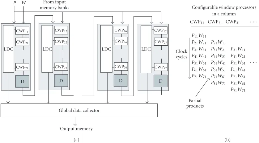
In this section some details of the proposed hardware ar-chitecture for window-based image processing are presented. The architecture exploits data parallelism and reuse through a column-based memory addressing mode and a set of pro-cessing elements working in parallel. The computation core of the architecture is organized under a 2D systolic array of processing elements. The processing element specially de-signed for the systolic architecture is called configurable win-dow processor (CWP).
The architecture is a stand-alone processor, but the mem-ories for storage of the input image and the processed image are external to the architecture. The architecture reads data from the input memory banks where input image pixels and
window mask coefficients are stored, denoted asPandW,
re-spectively. The image pixels are read in a column-based scan and they are transmitted to the array of processing elements to compute, in parallel, several window operations.
3.1. Array of configurable window processors
The array of processing elements is the computation core of the architecture. The processing elements are arranged
un-der a 2D systolic approach. Figure 4shows the 2D systolic
organization of the CWPs. The 2D systolic array extends the concurrency of the architecture to 2D parallelism, that is, the parallel computation of window operations through rows
and columns on the input image. InFigure 4, the module
de-noted by CWP represents a configurable window processor, the module labeled by D represents a delay line or shift regis-ter, and the module labeled with LDC represents a local data collector. For each column of the systolic array there is a lo-cal data collector that collects results of CWPs located in the same column of the array. The global data collector mod-ule collects the results and sends them to the output mem-ory. The CWPs in the same column, enclosed by a rectangle, compute a window operator on the same column of the in-put image. This set of CWPs can be considered as a 1D sys-tolic array. Data flows from top to bottom, and the CWPs work progressively in a systolic pipeline. The control module
and the address generator unit are not shown inFigure 4for
simplicity.
A delay line is required in the boundary of the CWPs in a column in order to support partial unrolling. The delay line is designed as a serial-input serial-output shift register.
Thus, the window coefficients are temporally stored in the
delay line, delayed for synchronization purposes, and then transmitted to the next column of CWPs. The stage number in the delay line depends on the loop unrolling degree
em-ployed. IfNRrows are processed in parallel, then a delay line
withNR−1 register is required because of a mismatch
be-tween the window mask size and the number of pixels read per column. In other words, the number of clock cycles
re-quired to all the coefficients of a column of the window mask
pass throw a column of CWPs isw+NR.
Afterw+NR clock cycles, the coefficients of the current
column of the window mask are sent progressively to the next
P W From input memory banks
LDC
CWP11
CWP21
CWP71
D
LDC
CWP12
CWP22
CWP72
D
LDC
CWP16
CWP26
CWP76
D
LDC
CWP17
CWP27
CWP77
D
Global data collector
Output memory
Clock cycles
Configurable window processors in a column
CWP11 CWP21 CWP31 · · ·
P11W11
P21W21
P31W31
P41W41
P51W51
P61W61
P71W71
P21W11
P31W21
P41W31
P51W41
P61W51
P71W61
P81W71
P31W11
P41W21
P51W31
P61W41
P71W51
P81W61
P91W71 · · ·
Partial products
(a) (b)
Figure4: (a) Systolic array for fast speed computing of window-based image operations. (b) Data flow and computation for some CWPs in the same column for image convolution.
mask is fed to the current set of CWPs. A detail of the data
flow of window mask coefficients through CWPs is shown in
Figure 4.
The local data collector collects data from the CWPs, and the captured result is sent out of the CWPs to a global data collector. The local data collector scans progressively the CWPs from top to bottom according to a control signal from the control unit module in the architecture.
The interconnection of several columns of CWPs towards a 2D systolic array extends the concurrency of the architec-ture to 2D parallelism by exploiting data parallelism through parallel processing, pipeline, and loop unrolling. The inter-connection between columns of CWPs is straightforward and it can be considered a cascaded connection of 1D sys-tolic arrays. In the 2D array, data flows from top to bottom of a column, and then left to right through columns.
As a whole, the architecture operation starts when a pixel from the input image is broadcast to all the processing ele-ments in the array. Each CWP working in parallel keeps track of a particular window-based operation. At each clock cycle,
a CWP receives a different window coefficient, stored in an
internal register, and an image pixel that is common for all the processing elements. These values are used by each CWP to carry out a computation, specified by a scalar function, and to produce a partial result of the window operation. The partial results are incrementally sent to the local reduction function implemented in the CWP to produce a single result
when all the pixels of the window are processed. InFigure 4
a detail of the data flow and the computation steps for three CWPs in the same column of the systolic array is shown for several clock cycles when the systolic array is configured for
image convolution with a 7×7 window mask. Each CWP,
if enabled, performs the computation of a multiplication and an accumulation.
After a short latency period, each CWP has progressively computed an output of a window operation. The produced result is captured by the data collectors and stored in the out-put image memory. Once a result produced by a CWP is col-lected, the processing element is ready to start a new com-putation. The CWPs work progressively in the same man-ner until all data in the input image has been processed. The CWPs are continuously being reutilized for computing dif-ferent windows in the input image.
3.2. Configurable window processor
Figure 5shows a simplified block diagram of the processing element designed to cover most window-based operations in image processing. It is called a configurable window proces-sor (CWP). The CWP is composed of a register, an arith-metic processor (AP), and a local reduction module (LRM). The AP is based on a similar scheme of an arithmetic logic unit (ALU) and provides the hardware support for the scalar functions. It includes a multiplier, an adder/subtracter, and a distance computation module. The LRM module imple-ments the local reduction function and it includes an accu-mulator and a maximum/minimum computation module. For instance, for image convolution, the AP module per-forms a multiplication and the LRM module perper-forms an accumulation. Similarly, for gray-level dilation/erosion, the AP module and LRM module perform additions/subtraction and maximum/minimum operations, respectively.
W P
Control word AP
z−1 LRM
Wd Pc
Figure5: Block diagram of the configurable window processor.
operational inputs, pixels from the input image, and coeffi
-cients from the window mask, denoted byPandW,
respec-tively. Each CWP has two output signals. One of them is the
result of the window operation (PC) and the other one is a
delayed value of a window coefficient (Wd) that is
transmit-ted to its neighbor CWP or to a delay line. The CWP accepts
one pixel data and a window coefficient to compute one step
of a window operation in a clock cycle.
The functionality of the CWP is configured by a control word in run time. The user sends a control word through a port of the architecture to control the operation that the AP and LRM must perform according to an application.
In summary, on each clock cycle, each CWP executes in parallel three disjoint operations:
(i) compute the pixel by pixel value to be passed to the next computation cycle,
(ii) integrate the contents of the output register, calculated at the previous clock cycle, with the new value pro-duced by the AP module,
(iii) read a new window coefficient and store it into the
reg-ister then, transmit the previous coefficient to the next
CWP.
4. COMPLEXITY AND PERFORMANCE ISSUES
The hardware architecture presented in the previous sections is dedicated to window-based image processing under real-time constraints. The main concerns for the architecture de-sign were a regular input data scheme with a small num-ber of data input/output ports, and fast parallel processing of window operations. In this section, some metrics are es-tablished to evaluate the complexity and performance of the architecture in term of architectural parameters. Throughout the analysis, it is considered that the proposed architecture
consists of NCWP(R) rows of configurable window
proces-sors. Each row includesNCWP(C) configurable window
pro-cessors.
4.1. Processing time
The required processing time to process an input image with a window-based operator is composed of two main times: the latency timeand theparallel processing time.
Thelatency timecorresponds to the time required to start pipeline operation inside the 2D systolic array. The latency time is measured between the activation of the first CWP un-til the activation of the last CWP. The latency is significant when the 2D systolic array starts the processing of a new set of rows of the input image.
The time required to initialize full pipeline operation of the parallel modules at the beginning of row processing is given by
τl=
(MaskSize−1)×NCWP(R) + MaskSize−1
×1 F ×
M NCWP(R)
, (5)
whereNCWP(R) is the number of rows processed in parallel,
MaskSizeis the size of mask used in the computations,Fis
the main clock frequency, M is the number of rows of the
image, andNis the number of columns of the image.
Theparallel processing timeis the time when all the CWPs in the 2D systolic array are working in parallel. This is the addition of all the computing times to process a set of rows, without considering the latency at the start of processing.
The required parallel processing time to processM×N
pixels, without the initial latency is given by
τp=M×N×
NCWP(R) + MaskSize−1
NCWP(R)
×1
F. (6)
The factor enclosed in brackets represents the average clock cycle number to produce a result. The overall time
needed to process an (M×N)-sized image is given by the
summation of the preceding times:
T=τl+τp. (7)
From the architectural point of view, the performance is compromised with the number of rows processed concur-rently, hence with the silicon resources allocated to the ar-chitecture.
4.2. Throughput
The throughput of a system can be expressed in terms of the number of elemental operations that the system can perform per second. In this sense, only the operations contributing to the computation of a result are considered. In the particular case of the architecture, two operations are of significance, the scalar function and the local reduction function executed on each clock cycle. Under these considerations, the compu-tational throughput of the architecture can be calculated ac-cording to the following equation:
Throughput=F×NCWP(R)×NCWP(C)
×NIPCWP, (8)
where Fis the main clock frequency, NCWP(R)×NCWP(C)
the number of processing elements in the systolic array, and
NIPCWPthe average number of elemental operations
The NIPCWPparameter denotes the efficiency degree of computational usage of each CWP in the 2D systolic array.
The NIPCWP depends on the topology of the systolic array
and the dimension of the problem to be solved. The NIPCWP
can be computed according to the following equation:
NIPCWP=2× MaskSize
NCWP(R) + MaskSize−1
, (9)
where MaskSize denotes the dimension of the window used in the window-based image operator.
5. RESULTS
To achieve the required characteristics related to the architec-ture performance and configurability, a fully parameterizable VHDL description of the modules of the proposed archi-tecture was carried out by making extensive use of generic-type configurations inputs. Furthermore, a fully structural description of these modules was also carried out, using only the most elementary logic operations provided by the imple-mentation library to achieve good optimization levels for the main components of the architecture. Since structural VHDL was used for a hierarchical design, the whole design is plat-form, version, technology, and tool independent.
The modules and the complete architecture were synthe-sized with the XST tool and placed and routed with Foun-dation ISE from Xilinx. All the simulations were carried out with Active HDL, both functional and postsynthesis simula-tions.
5.1. Hardware resource utilization
This section presents the FPGA synthesis results for the main modules of the architecture. The hardware resource utiliza-tion is reported for an XCV2000E-6 VirtexE FPGA device. The digital synthesis was carried out in a hierarchical and
in-cremental way. The results are summarized inTable 2, using
as main parameters the number of slices, and specifically the number of flip-flops and look-up tables of the FPGA.
The results shown inTable 2were obtained with the XST
synthesis tool configured to optimize for speed. A 7×7
sys-tolic array of CWPs was synthesized. Since no temporal re-strictions of low-level were imposed on the place and route process, further improvements in area and speed can be ob-tained if timing and area restrictions are imposed. The hard-ware resource utilization is only a small part of the FPGA re-sources, about 30 percent. In fact, the architecture suits well for FPGAs with lower logic capacities.
An available prototype of the architecture, synthesized for an XCV2000E-6 Virtex device, executes approximately
3.16 GOPs at a 60 MHz clock frequency. The hardware
ar-chitecture was prototyped using an RC1000PP FPGA-based board from Alpha Data. The FPGA-based board is centered on a VirtexE device with an equivalent logic capacity of 2 million gates. The board is attached to the PCI bus of a host computer, and it contains 8 MB on-board memory organized in four banks of 2 MB each. The memory and hardware re-sources available in the board can be accessed through an
Table2: FPGA synthesis summary for the architecture and its main modules.
XCV2000E-6 FPGA VirtexE device
Module Number of 4-input Number of slices LUTs flip-flops CWP
101 190 24
address Generator
154 269 97
unit
Control unit 5 10 3
A column of
840 1506 223
7 CWPs Complete
6118 10734 1604
architecture
Table3: Technical data for the systolic architecture for real-time window-based image processing. The architecture was synthesized for a 7×7 systolic array.
Technical data for the systolic architecture XCV2000E-6 FPGA Virtex device Feature Specification
FPGA technology 0.18µm 6-layer metal process
Power supply 1.8 V Number of processing
49 elements, CWPs
Clock frequency 60 MHz FPGA percentage for the
6118 slices, around 30% complete architecture
FPGA percentage per
101 slices, less than 1% CWP
FPGA percentage, address
159 slices, less than 1% and control logic
Number of flip-flops 1604 Estimated power
1.56 W consumption
Off-chip memory data
21-bit address, 8-bit data buses
On-chip memory 81 8-bit registers Peak performance 3.16 GOPs Number of pins 92
API developed in Visual C++. An experimental setup for ar-chitecture prototyping with real images was built using this board.
A summary of the technical data for the FPGA imple-mentation of the current architecture prototype, highlight-ing aspects such as technology, hardware resources,
perfor-mance, and power consumption, is shown in Table 3. The
current prototype is based on a systolic array of 7×7 CWPs.
35 30 25 20 15 10 5
P
roc
essing
time
(ms)
0 2 4 6 8 10 12 14 16 18 20
Number of rows processed in parallel
Figure6: Architecture performance with different parallelism de-grees.
5.2. Performance
In this section the results of the processing time of the pro-posed architecture for performing window-based operators on an input image are presented. The results and graphs were obtained using the synthesis results and the equations
pre-sented and discussed inSection 4.
Figure 6 shows the processing time of the architecture versus the number of rows processed in parallel. Per each
row, a set ofMaskSizeCWPs is employed in the 2D systolic
array. The processing time is the time required to process an image on the proposed architecture when image data is al-ready available in the input image memory. All the additional
times needed for theI/Orequests and data transfers are not
considered in the performance analysis of the architecture since they are dependent on the prototyping platform. Thus, the image acquisition overhead must be added to the pro-cessing time. However, the image acquisition overhead can be overcome in a hardware prototyping platform if an
ap-propriate double buffering is employed, that is, the
acquisi-tion process is performed concurrently with the processing using independent memory banks.
A 512×512 image and a 7×7 window mask were
consid-ered to plot the curves inFigure 6. An increase in the number
of CWPs produces an increase in the overall performance of
the architecture. As can be seen fromFigure 6, a systolic array
with the capability of processing two rows in parallel would be enough to fulfil real-time requirements, that is, processing of 30 frames per second.
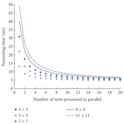
The processing times for a window-based operation on
512×512 gray-level images using different window sizes are
plotted inFigure 7. The image processing time using a 7×7
window mask is 8.35 milliseconds, which leaves time for
im-age acquisition or imim-age memory loading since about 30 milliseconds are required to achieve standard real-time con-straints. Moreover post-processing on the resulting image
can be applied. The performance results for different window
sizes are plotted on the same figure. The 2D systolic array was
50 45 40 35 30 25 20 15 10 5 0
P
roc
essing
time
(ms)
0 2 4 6 8 10 12 14 16 18 20
Number of rows processed in parallel 3×3
5×5 7×7
9×9 11×11
Figure7: Performance of the proposed architecture for a 512×512 gray-level image with different window sizes where the array has an equal dimension to window mask.
5 4.5 4 3.5 3 2.5 2 1.5 1 0.5
Giga
oper
ations
per
sec
ond
0 2 4 6 8 10 12 14 16 18 20
Number of rows processed in parallel
Figure8: Throughput of the architecture for different configura-tions of the 2D systolic array.
configured to use the same number of processing elements as the window size. For all the cases, it is possible to achieve real-time performance with low hardware resource utilization.
Figure 8shows the achievable throughput of the
architec-ture when different parallelism degrees, number of
process-ing elements, are employed. The graph shows the number of GOPs versus the processing elements employed. As can be seen, the throughput increases with the number of process-ing elements. However, if many processprocess-ing elements are used
in the systolic array the utilization and activity efficiency of
A performance improvement can be obtained-either op-timizing the design mapped onto the FPGA or employing an FPGA built with a better semiconductor technology. How-ever, the performance of the architecture fulfils the real-time requirements and provides the advantages of compactness and scalability for further improvements. The results pre-sented in this section can be used for rough estimation of hardware resource utilization and evaluation of the architec-ture performance. For reliable comparisons with other sys-tems and architectures, it would be necessary to use the same fabrication technology and equal amount of silicon area since smaller geometries allow packing more computation into the
silicon area [13].
6. DISCUSSION
In this section, the window-based operation performance on the proposed architecture is compared with other currently available architectural solutions. Comprehensively compar-ing image processcompar-ing hardware architectures is undoubtedly
a complex task for a single research effort. Moreover, the lack
of standard metrics increases the complexity to do reliable comparison. There are several parameters for comparison and performance evaluation of hardware architectures and systems. Some common parameters used in the literature for comparison purposes are processing speed normalized for chip area, power consumption, operation throughput, data
transfer efficiency, parallel efficiency, and the product of the
number of processing elements and the processing time for
one frame [7,10]. However most of the metrics are rarely
reported in the literature for architectures and systems.
6.1. Comparison with other architectures
The first way to make a fair comparison between the pro-posed architecture and other image processing architectures is within the application scope of window-based operations. The same set of algorithms should be performed on each ar-chitecture to standardize the metric for performance. Among the window-based image algorithms mapped into the systolic architecture are image convolution, template matching, and gray-level image morphology.
The comparisons made on this work are intended to be
performed among several different array processor
architec-tures. In order to do fair comparison, the architectures are compared under same conditions as
(i) they are used to deal with the same algorithm class, (ii) the same image size is used, unless another case is
es-tablished,
(iii) the execution time, clock cycles, is used as the main metric for comparison, since a lack of other metrics reported in literature.
The timings for some window-based image operators
and their corresponding implementations on different
hard-ware architectures are summarized inTable 4. In the table,
the window-based image application, the machine architec-ture, image size, and processing time are used as main
pa-rameters for comparison [7,8,15,16,17,18].
The architecture performance is similar and even better than other architectures and systems reported in the
liter-ature, as shown inTable 4. Since the architecture is not an
ASIC, its performance regarding ASIC architectures is signif-icant without sacrificing flexibility. Moreover, if the proposed architecture is implemented in an ASIC, it will provide a per-formance improvement of one order of magnitude.
The architecture provides a high throughput, 3.16 GOPs
with power consumption of about 1.56 W and the processing
time is independent of the window-based algorithm mapped to the architecture. Regarding power consumption, the archi-tecture provides an improvement over two magnitude orders over Pentium processors. The power consumption of Pen-tium IV is about 70 W.
6.2. Area/performance tradeoffs
In order to analyze the requirements of area for different
configurations of the architecture, a graph of the number of FPGA hardware resources used versus a particular
window-based application was obtained. As shown in Figure 9, the
hardware resources, number of LUTs, slices, and flip-flops in the FPGA depend on a particular window-based image appli-cation mapped to the FPGA. The most hardware demanding application is the convolution since it requires a multiplier per each CWP in the array to perform the operation.
From Figure 9, it can be shown that it is possible to achieve real-time performance for window-based image pro-cessing with very compact architectures. The low resource utilization allows the architecture to be implemented in com-pact mobile applications restricted to low-power consump-tion. From results presented above, it is clear that the
pro-posed architecture obtains a very high efficiency, and it is
possible to state that it provides a high computational den-sity due to the relatively small implementation area used of the FPGA. Furthermore, since the current architecture con-figuration provides a computational power greater than that required for real-time performance, it is possible to reduce at some extent the hardware resources or the main clock fre-quency for power saving purposes.
6.3. Multifunctional architecture
One of the main advantages of the proposed architecture is its configurability. The architecture is flexible enough to support several variations of window-based image operators.
Thus, the architecture offers the possibility of addressing
dif-ferent image-based applications from the system-on-a chip (SoC) perspective.
Due to its versatile, modular, and scalable design, the ar-chitecture constitutes a platform to explore more complex algorithms such as block matching for motion estimation, stereo disparity computation, and discrete cosine transfor-mation, among others. Some of these potential applications are currently being developed. For instance, the following key aspects have to be considered in order to map a block
match-ing algorithm into the architecture. First, the coefficients of
the window mask are variable and their values are obtained of windows extracted from the reference image. Second, once
Table4: Performance comparison of the architecture with other proposed systems for window-based image processing.
Performance benchmarks on different architectures
System Architecture Application Image size Timing
TMS320C80 Multiprocessor 5×5 Gaussian convolution 512×512 40 ms TMS320C80 Multiprocessor 3×3 gray-level dilation 512×512 32.7 ms
Splash 2 Multi-FPGA 3×3 median filter 512×512 27 ms
PDSP16488 40 MHz Hardwired ASIC 8×8 convolution 512×512 6.56 ms PPIP 64×64 2D SIMD array 5×5 Laplacian filter 512×512 197µs PPIP 64×64 2D SIMD array 5×5 Gaussian convolution 512×512 730µs LSI Logic’s L64240, 20 MHz Hardwired ASIC 8×8 convolution 512×512 13.11 ms Blue wave system PCI/C6200 DSP-based, 3×3 convolution 512×512 7.2 ms Alacron’s AI-860 I860 processor 8×8 convolution 512×512 66.1 ms
UWGSP5 DSP-based, MVP 3×3 convolution 512×512 19 ms
IMAP vision SIMD, 256 PE 3×3 convolution 256×256 0.65 ms IMAP vision SIMD, 256 PE 3×3 gray-level dilation 256×256 0.31 ms DECChip 21064 Multiprocessor 5×5 convolution 512×512 220 ms MAP1000 200 MHz Media processor VLIW 7×7 convolution 512×512 7.9 ms VP24000/10 Vector computer 8×8 template matching 512×512 40 ms 500 MHz Pentium III Superscalar 8×8 convolution 512×512 56.5 ms
Proposed architecture Systolic 7×7 generic window-based 512×512 8.35 ms image operator
12000 10000 8000 6000 4000 2000 0
F
P
G
A
h
ardw
are
re
so
u
rce
s
Complete Convolution Template matching
Morphology
LUTs Slices Flip-flops
Figure9: FPGA hardware resources for different architecture con-figurations.
the search area associated to the reference image. Similarly, the stereo matching can be formulated as a window operator
such as the block matching. The difference for this case is that
two static images from two points of view are considered.
7. CONCLUSIONS
This paper has presented an alternative and flexible FPGA-based architecture for window-FPGA-based image processing under real-time constraints. A set of processors is organized under a
systolic approach to form a programmable architecture. The
architecture can achieve a processing rate of near 3.16 GOPs
with a 60 MHz clock frequency. The high-performance and compact hardware architecture opens new and practical pos-sibilities to mobile machine vision systems where size and power consumption are hard constraints to overcome. The architecture was derived from a functional decomposition of window-based algorithms and operators. In order to cope with a broad class of image processing algorithms, a com-putational processing unit, called configurable window pro-cessor, was defined.
The programmability of the proposed architecture pro-vides the additional advantage of being more flexible than the ASICs based on hardwired approaches. The configurable window processor developed in this research can be used and
adapted to support different algorithms based on a window
processing scheme. The window-based image processing al-gorithms addressed in this research include generic convolu-tion, template matching, and gray-level image morphology. Moreover, some other applications suit well for the architec-ture such as block matching for motion estimation, stereo disparity computation, among others. In this sense, a soft-ware tool will be explored to synthesize dedicated modules for low-level image processing using as a basis the addressing mode and the parallel techniques employed in the proposed architecture.
REFERENCES
[1] R. Jain, R. Kasturi, and B. G. Schunck, Machine Vision, McGraw-Hill, New York, NY, USA, international edition, 1995.
[2] N. Ranganathan, Ed., VLSI & Parallel Computing for Pattern Recognition & Artificial Intelligence, vol. 18 ofSeries in Ma-chine Perception and Artificial Intelligence, World Scientific Publishing, 1995.
[3] P. A. Laplante and A. D. Stoyenko, Eds., Realtime Imaging -Theory, Techniques and Applications, IEEE Press, New York, NY, USA, 1996.
[4] P. M. Athanas and A. L. Abbott, “Real-time image processing on a custom computing platform,” Computer, vol. 28, no. 2, pp. 16–24, 1995.
[5] J. Silc, T. Ungerer, and B. Robic, “A survey of new research directions in microprocessors,”Microprocessors and Microsys-tems, vol. 24, no. 4, pp. 175–190, 2000.
[6] M. K. Ratha, Computer Vision Algorithms on Reconfigurable Logic Arrays, Ph.D. Dissertation, Michigan State University, 1996.
[7] B. Bosi, G. Bois, and Y. Savaria, “Reconfigurable pipelined 2-D convolvers for fast digital signal processing,” IEEE Trans. VLSI Syst., vol. 7, no. 3, pp. 299–308, 1999.
[8] R. Managuli, G. York, D. Kim, and Y. Kim, “Mapping of two-dimensional convolution on very long instruction word me-dia processors for real-time performance,” Journal of Elec-tronic Imaging, vol. 9, no. 3, pp. 327–335, 2000.
[9] D. H. Ballard and C. M. Brown, Computer Vision, Prentice-Hall, Englewood Cliffs, NJ, USA, 1982.
[10] D. Li, L. Jiang, and H. Kunieda, “Design optimization of vlsi array processor architecture for window image processing,” IEICE Transactions on Fundamentals of Electronics, Commu-nications and Computer Sciences, vol. E82-A, no. 8, pp. 1475– 1484, 1999.
[11] A. Bouridane, D. Crookes, P. Donachy, K. Alotaibi, and K. Benkrid, “A high level FPGA-based abstract machine for image processing,”Journal of Systems Architecture, vol. 45, no. 10, pp. 809–824, 1999.
[12] V. Moshnyaga, N. Watanabe, and K. Tamaru, “A memory effi -cient array architecture for real-time motion estimation,” IE-ICE Transactions, vol. J81-D-I, no. 2, pp. 77–85, 1998. [13] A. DeHon, “The density advantage of configurable
comput-ing,”Computer, vol. 33, no. 4, pp. 41–49, 2000.
[14] P. Marchal, “Field-programmable gate arrays,” Communica-tions of the ACM, vol. 42, no. 4, pp. 57–59, 1999.
[15] M. Arias-Estrada and C. Torres-Huitzil, “Real-time field pro-grammable gate array architecture for computer vision,” Jour-nal of Electronic Imaging, vol. 10, no. 1, pp. 289–296, 2001. [16] B. Draper, W. Najjar, W. B¨ohm, et al., “Compiling and
op-timizing image processing algorithms for FPGA’s,” in Inter-national Workshop on Computer Architecture for Machine Per-formance (CAMP ’00), pp. 240–246, Padova, Italy, September 2000.
[17] F. Lohier, M´ethodologies de programmation et ´evaluation des processeurs de traitement de signal paralleles por le traitement d’images en temps r´eel, Ph.D. Dissertation, L’Universite Pierre Et Marie Curie (Paris 6), 2000.
[18] H. Singh, M.-H. Lee, G. Lu, F. J. Kurdahi, N. Bagherzadeh, and E. M. Chaves Filho, “Morphosys: an integrated recon-figurable system for data-parallel and computation-intensive applications,” IEEE Trans. Comput., vol. 49, no. 5, pp. 465– 481, 2000.
C´esar Torres-Huitzilreceived his B.S. de-gree in electronic engineering from the Uni-versidad Aut ´onoma de Puebla (BUAP) in 1995, and his M.S. degree in electronics and his Doctor degree in computer science from the National Institute for Astrophysics, Op-tics and Electronics (INAOE), Puebla, Mex-ico, in 1998 and 2003, respectively. Since 1998, he is a Researcher of the Digital Sys-tems Design Group in the Electronics
Fac-ulty, BUAP. Currently, he is a Postdoctoral Fellow at Laboratoire Lorrain de Recherche en Informatique et ses Applications (LORIA), France. His research activities include work on computer vision ar-chitectures for real-time operation, reconfigurable computing, evo-lutionary computation, and HDL modeling of digital systems. The current emphasis of his work is on FPGA implementation of high-density neural networks.
Miguel Arias-Estradareceived the B.Eng. degree in communications and electron-ics, and the M.Eng. degree in electronics from the Universidad de Guanajuato, Mex-ico, in 1990 and 1992, respectively, and the Ph.D. degree in electrical engineering from the Universit´e Laval in Quebec, Canada, in 1998. From 1997 to 1998, he was with the Electrical and Computer Engineering De-partment, Universit´e Laval in Canada. Since