ISSN (Print) : 2320 – 3765 ISSN (Online): 2278 – 8875
I
nternational
J
ournal of
A
dvanced
R
esearch in
E
lectrical,
E
lectronics and
I
nstrumentation
E
ngineering
(A High Impact Factor, Monthly, Peer Reviewed Journal)
Website: www.ijareeie.com
Vol. 7, Issue 6, June 2018
Implementation of AM and DSB-SC
Modulation Techniques on FPGA
Dr. R. Prakash Rao
Associate Professor, Department of Electronics and Communication Engineering, Matrusri Engineering College,
#16-1-486, Saidabad, Hyderabad, India
.
ABSTRACT: This research work explicates the various simulation results using Simulink and System Generator and its implementation on FPGA. Initially the most important analog modulation techniques which are AM and DSB-SC modulation techniques are elucidated. Afterwards these modulation techniques are constructed and tested with in Simulink. Prior to realization of this design within System Generator the audio signal is imported to the Simulink and the simulation results are investigated on FPGA.
KEYWORDS: Simulink, System Generator, FPGA, AM and DSB-SC.
I.INTRODUCTION
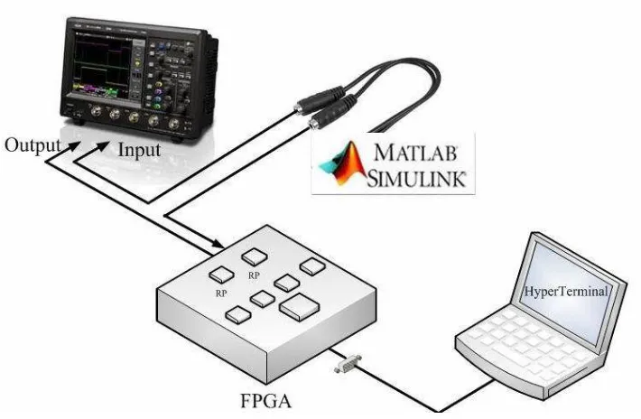
In the following steps, Simulink is used to generate an input sine signal that was transmitted through wire connection to the FPGA, and finally the output result was captured on an oscilloscope. This configuration is illustrated in Figure 1.
ISSN (Print) : 2320 – 3765 ISSN (Online): 2278 – 8875
I
nternational
J
ournal of
A
dvanced
R
esearch in
E
lectrical,
E
lectronics and
I
nstrumentation
E
ngineering
(A High Impact Factor, Monthly, Peer Reviewed Journal)
Website: www.ijareeie.com
Vol. 7, Issue 6, June 2018
II. DSB-SC MODULATION AND ITS RESULTS
DSB-SC modulation is implemented on the FPGA which is shown in Figure 2. The processing of implementing this modulation is conducted within System Generator by generating netlist file and then used the generated netlist file for generating partial bitstreams in PlanAhead. Figure 3 shows the input signal and the modulated signal of DSB-SC modulation. In this figure, the signal in the upper portion of the figure represents the input sine wave which is generated from Simulink and lower signal shows the output signal of the FPGA [1]. The carrier frequency is generated within System Generator by DDS block.
Fig 2. DSB-SC Modulation Process
In addition, this configuration was tested with an audio signal input, and the output signal was observed on the oscilloscope [2]. Figure 4 shows the output results of a DSB-SC modulated of an audio signal on the FPGA. The results in this section are compared with the Simulink and the System Generator simulation results which show the similar results among all of them [3].
ISSN (Print) : 2320 – 3765 ISSN (Online): 2278 – 8875
I
nternational
J
ournal of
A
dvanced
R
esearch in
E
lectrical,
E
lectronics and
I
nstrumentation
E
ngineering
(A High Impact Factor, Monthly, Peer Reviewed Journal)
Website: www.ijareeie.com
Vol. 7, Issue 6, June 2018
(a) (b)
Fig 4. Output Results of Modulated Signal (DSB-SC Modulation) on the FPGA (a) 0ms Sec/Div (b) 5ms Sec/Div
III. ANALOG MODULATION AND ITS RESULTS
Similarly, the next implemented modulation technique is modulating an AM signal which is shown in Figure
5. In this figure, Constant1 block with value of 0.5 represents ka for AM modulation [4]. The input signal and output
result of this modulation was captured on the same oscilloscope.
Figure 6 illustrates the output result of this modulation process. Again, the signal in the upper portion of this figure represents the input sine signal which is generated from Simulink and lower signal shows the output modulated signal [5]. The carrier frequency is generated within System Generator by DDS block. Moreover, this configuration was tested with an audio signal input and the output signal was captured on the oscilloscope which is shown in Figure 7.
The results of these measurements after implementation on an FPGA well matched to the simulation results of Simulink and System Generator which shows this reconfigurable system.
ISSN (Print) : 2320 – 3765 ISSN (Online): 2278 – 8875
I
nternational
J
ournal of
A
dvanced
R
esearch in
E
lectrical,
E
lectronics and
I
nstrumentation
E
ngineering
(A High Impact Factor, Monthly, Peer Reviewed Journal)
Website: www.ijareeie.com
Vol. 7, Issue 6, June 2018
In the next configuration, the entire of DSB-SC modulation and demodulation is implemented within a same module which is shown in Figure 8. This figure shows that the carrier frequency is generated within System Generator by DDS block and then directly multiplied by the input signal (message signal).
Fig 6. Output Results of Modulated Signal (AM Modulation) on the FPGA (1) Input Signal (2) Output Signal
Fig 7. Output Results of Modulated Signal (AM Modulation) on the FPGA (1) Input Audio Signal (2) Output Audio Signal
ISSN (Print) : 2320 – 3765 ISSN (Online): 2278 – 8875
I
nternational
J
ournal of
A
dvanced
R
esearch in
E
lectrical,
E
lectronics and
I
nstrumentation
E
ngineering
(A High Impact Factor, Monthly, Peer Reviewed Journal)
Website: www.ijareeie.com
Vol. 7, Issue 6, June 2018
is captured on the oscilloscope which is shown in Figure 10. The results of these measurements well matched to the simulation results of Simulink and System generator.
Fig 8. Entire DSB-SC Modulation and Demodulation on a Same Module
ISSN (Print) : 2320 – 3765 ISSN (Online): 2278 – 8875
I
nternational
J
ournal of
A
dvanced
R
esearch in
E
lectrical,
E
lectronics and
I
nstrumentation
E
ngineering
(A High Impact Factor, Monthly, Peer Reviewed Journal)
Website: www.ijareeie.com
Vol. 7, Issue 6, June 2018
Fig 10. Output Results of DSB-SC Modulation on the FPGA (1) Input Audio Signal (2) Output Audio Signal
In the next configuration, entire AM modulation and demodulation is implemented within a same module which is shown in Figure 11.
ISSN (Print) : 2320 – 3765 ISSN (Online): 2278 – 8875
I
nternational
J
ournal of
A
dvanced
R
esearch in
E
lectrical,
E
lectronics and
I
nstrumentation
E
ngineering
(A High Impact Factor, Monthly, Peer Reviewed Journal)
Website: www.ijareeie.com
Vol. 7, Issue 6, June 2018
In this figure, the FIR Compiler 5.0 and Xilinx FDAtool are used to remove higher frequency components of the recovered signal [8]. The output result of this modulation process is illustrated in Figure 12. Again, the signal in the upper portion of this figure represents the input sine signal which is generated from Simulink and lower signal shows the recovered signal after demodulation process. The carrier frequency is generated within System Generator. Also, this configuration was tested with an audio signal input and the output signal was captured on the oscilloscope which is shown in Figure 13. The results of these measurements are similar to the simulation results of Simulink and System generator in previous chapter.
In the following step, a DSB-SC modulated signal is generated within Simulink and transmitted to the FPGA through a wire connection [9]. The FPGA now works as a DSB-SC demodulator (radio receiver). The implementation of this demodulation is illustrated in Figure 14. The output result of this demodulation process is shown in Figure 15.
Fig 12. Output Result of AM Modulation on the FPGA (1) Input Signal (2) Output Signal
Fig 13. Output Result of AM Modulation on the FPGA (1) Input Signal (2) Output Signal
ISSN (Print) : 2320 – 3765 ISSN (Online): 2278 – 8875
I
nternational
J
ournal of
A
dvanced
R
esearch in
E
lectrical,
E
lectronics and
I
nstrumentation
E
ngineering
(A High Impact Factor, Monthly, Peer Reviewed Journal)
Website: www.ijareeie.com
Vol. 7, Issue 6, June 2018
Fig 14. DSB-SC Demodulator (Radio Receiver) in System Generator
Fig 15. Output Result of DSB-SC Demodulation on the FPGA (1) Input Signal (2) Output Signal
ISSN (Print) : 2320 – 3765 ISSN (Online): 2278 – 8875
I
nternational
J
ournal of
A
dvanced
R
esearch in
E
lectrical,
E
lectronics and
I
nstrumentation
E
ngineering
(A High Impact Factor, Monthly, Peer Reviewed Journal)
Website: www.ijareeie.com
Vol. 7, Issue 6, June 2018
REFERENCES
1. “Simulink - Simulation and Model-Based Design,”
http://www.mathworks.com/products/simulink/. .
2. Percey, Advantages of the Virtex-5 FPGA 6-Input LUT Architecture. San Jose, CA: Xilinx,
Inc., 2007.
3. “Genesys Virtex, 5 FPGA Development Kit,” http://www.digilentinc.com/Products/Detail.cfm?@avPath=2,400,819&Prod=GE@ ESYS. .
4. “Virtex-5 OpenSPARC Evaluation Platform,” http://www.digilentinc.com/Products/Detail.cfm?Prod=XUPV5&@av1=Products&
@av2=Programmable. .
5. P. Sirisuk, Reconfigurable Computing: Architectures, Tools and Applications: 6thInternational Symposium, ARC 2010, Bangkok, Thailand,
March 17-19, 2010, Proceedings. Springer, 2010.
6. “Xilinx University Program,” http://www.xilinx.com/university/index.htm.
7. . P.-A. Hsiung, M. D. Santambrogio, and C.-H. Huang, Reconfigurable SystemDesign and Verification, 1st ed. CRC Press, 2009.
8. “POWER to the people,” http://www.ibm.com/developerworks/power/library/pa-powerppl/, 15-Dec-2005.
9. .“High-Performance FPGA Architecture,”
http://www.altera.com/products/devices/stratix-fpgas/about/fpga-architecture/stx-architecture.html?GSA_pos=3&WT.oss_r=1&WT.oss=FPGA%20technology%20L ogic%20Array%20Blocks. .
10. R. Woods and J. McAllister, FPGA-based implementation of signal processingsystems. John Wiley and Sons, 2008.
11. B. Zeidman, Designing with FPGAs and CPLDs. Focal Press, 2002.