Available Online at www.ijcsmc.com
International Journal of Computer Science and Mobile Computing
A Monthly Journal of Computer Science and Information Technology
ISSN 2320–088X
IJCSMC, Vol. 3, Issue. 10, October 2014, pg.768 – 776
RESEARCH ARTICLE
Implementation of Different Operations
for Data Transfer for AMBA-Advanced
High Performance Bus
Tadikonda Nagarjuna
1, B.Anil Kumar
21M.Tech Student, Department of ECE, SSIT College of Engineering and Technology, JNTU, Hyderabad, India
2Assistant Professor, Department of ECE, SSIT College of Engineering and Technology, JNTU, Hyderabad, India
ABSTRACT:
This paper basically described the different operation of data transfer between two IPcores inAMBA Advanced High Performance Bus. This operations are such as simple read/write operation, burst read/write operation and out of order read write operation. Most of the IP cores from ARM use AMBA (Advanced Microcontroller Bus Architecture) which has AHB (Advanced High-Performance Bus), ASB (Advanced System Bus), and APB (Advanced Peripheral Bus). These buses are defines a system on-chip communication standard for designing high-performance embedded Microcontrollers The purpose of this paper work is to choose a SOC bus for Open Cores that we would adopt and use in any core development. The AHB (Advanced High-performance Bus) is a high High-performance bus in AMBA (Advanced Microcontroller Bus Architecture) family. This AHB can be used in high clock frequency system modules. This bus can be worked as the high-performance system backbone bus. It supports the efficient connection of processors, on-chip memories and off-chip external memory interfaces with low-power peripheral macro cell functions. In this work the basic building blocks of AHB (Master, Slave Arbiter, and Decoder) is developed using Verilog in Modelsim 6.6c.
INTRODUCTION
the proper and lossless communication between the IP cores which uses same protocols on the System on Chip (SOC) system. Basically, a SOC is a system which is considered as a set of components and interconnects among them. In this paper the basic building blocks of AHB (Master, Slave, Arbiter, and Decoder) are designed and simulated using Modelsim 6.4a.
Hence to resolve this issue, the standard protocol buses are used in or order to interface the two IP cores. Here the loss of data depends on the standards of protocols used. Most of the IP cores from ARM use the AMBA (Advanced Microcontroller Bus Architecture) which has AHB. (Advanced High- Performance Bus). This bus has its own advantages and flexibilities.
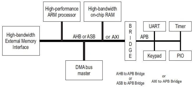
Fig.1 AMBA based Microcontroller
Figure 1 shows basic block diagram of AMBA based Microcontroller which consist of a high performance system backbone bus (AMBA AHB or AMBA ASB), able to sustain the external memory bandwidth, on which the CPU, on - chip memory and other Direct Memory Access (DMA) devices reside. This bus provides a high-bandwidth interface between the elements that are involved in the majority of transfers. Also located on the high performance bus is a bridge to the lower bandwidth APB, where most of the peripheral devices in the system are located.
AHB INTERCONNECTION
AHB is a new generation of AMBA bus which is intended to address the requirements of high performance synthesizable designs. It is a high performance system bus that supports multiple bus masters and provides high-bandwidth operation. AMBA AHB implements the features required for high-performance, high clock frequency systems including: burst transfers single-cycle bus master handover Wider data bus configurations (64/128, up to 1024 bits).
has to be active during the operation based on the address given by the master. A central decoder is also required to control the read data and response signal multiplexor, which selects the appropriate signals from the slave that is involved in the transfer. These make the read and write operation smoothly. The AMBA-Advanced High Performance Bus can support up to 16 Masters and 16 Slaves. Figure 2 illustrates the structure required to implement an AMBA AHB design with four masters and four slaves. In Figure 2 shows connection for the Masters and Slaves and for proper data transfer Matrix interconnection is required which includes Arbiter, Decoder and Multiplexer.
Fig.2 AHB interconnection diagram
The Figure 2 show the basic interconnection diagram
OPERATIONS IN AHB FOR DATA TRANSFER
SIMPLE READ WRITE OPERATION
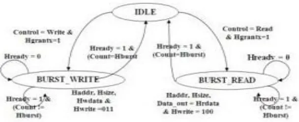
The Finite State Machine (FSM) for the AHB master simple write and read operation is developed and is shown in the Figure 3
Fig.3 FSM for AHB master for simple read write operation
AHB Master will be in IDLE State at the initial stage and will give the request signal to the arbiter which in turn provides the grant signal. Hence based on the control and the grant signal, AHB Master either goes to WRITE or READ state.
If control from the system is a write request (Control = “001”), then the AHB Master go WRITE state and will issue the address (HAddr) and input data (HWData) to the slave and also makes the HWrite signal “001”. Once these signals are issued, it will wait for the HReady signal which will come from the slave after finishing the operation. Once the HReady signal occurred, then the AHB Master will go to the IDLE state again.
Similarly, when system gives read request (Control = “010”), master goes to the READ state and will give address (HAddr) and make Hwrite signal “010”. The data in the given address will be read out by the output signal. Master go IDLE state when the HReady signal is made high which represents the operation got over.
Initially, all four AHB slave will be inactive and it will get activated by the Select (HSelx) signal from the decoder which in turn based on the given address (HAddr). Once the slave is activated, based on HWrite status, slave may go either WRITE or READ state. The developed FSM for the AHB slave is shown in the Figure 4.
Fig.4 FSM for AHB Slave for simple read write operation
BURST READ WRITE OPERATION
The Burst operation in AHB has the mandatory signals such as HSize and HBurst. Basically, AHB burst operation is that a sequence of operation happens with respect to the HSize given and it supports only three burst sizes which are mentioned in Table below. The size is acting as one of the inputs to the master during the burst operation and after each burst operation, the master or slave will go to the IDLE state.
FSM developed for the AHB Master – Burst operation is shown in the Figure 4 which has the clear view on the operation in a sequence manner. When write request (Control = “011”) is given and the arbiter provides the grant signal in response to request signal, AHB Master goes to WRITE state. Here the count signal is added which will be incremented only when the HReady signal made high i.e. count increments after each operation and will remain in the same state. When burst size is equal to the count, then the master go IDLE state that represents burst operation is over.
In Read operation, read request (Control = “100”) is given which leads to the master to READ state in which the stored data in the memory is read out with respect to the given address to the slave.
This output data is sent out through data_out signal and when count is equal to the burst size
OUT OF ORDER OPERATION
FSM and all function in this operation is same as in the burst read write operation except the increment of address. In this operation address is incremented by 2. Which means we can write or read the data from the odd memory location or write or read the data from the even memory location.
SIMULATION RESULT
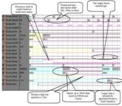
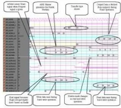
There are four Masters and four Slaves are present in the design in which one can be selected at a time by Arbiter and Decoder respectively. The simulation result for AHB Master and Slave - Simple Write and Read is shown in the Figure 5 and Figure 6 respectively and Figure 7 shows simple read write operation between Master and Slave.
Figure 6 Simulation result for Master Simple Read Write
The complete operation is Shown in Figure 6 Here in the waveform, Master is enabled which sends the request to the Arbiter which in turn provides the grant signal. Then the Master gives the Haddr, Hwdata and Hwrite =001 or Hwrite = 010 based on the current operation. This information are given to slave through „Address and Write Data Mux whose select line will be given by the Hmaster signal that represents which Master is currently selected. During the write operation write data Mux is activated and during read operation read data Mux is activated. The Slave will be activated with respect to the given address by the Decoder.
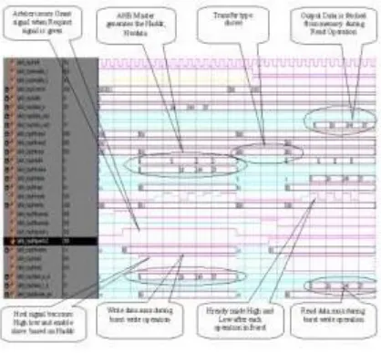
Figure 7 SIMPLE READ & WRITE operation
The simulation result for the AHB master and slave of burst size 4 is shown in the Figure 7 the size is given as “000” which represents the burst size 4 and hence four continuous write or read operation happens. Here the count is introduced in order to generate the address with respect the given initial address and the count increment. The operation remains the same as simple read and write but the only change is that after each operation, count will check for the burst size. When the count is not equal to the burst size given, the count will get incremented and the next address is generated based on which the read or write operation that currently performed is carried out. When the count is equal to burst length, that represents the burst operation over and count resets to zero. Hence master and slave go IDLE state.
The FSM for AHB Slave Out of order operation is same as in the burst operation. In IDLE state Hready will be made low and when Hwrite = 101 slave will go WRITE state and check for the count. The will get increment only when the data is stored in the memory and if count is equal to the burst size, then the slave will go to the IDLE state or it will stay in the WRITE state itself. In the same way, when Hwrite = 110, slave will go READ state and the data is fetched from Memory. In this operation the address location is also incremented by 2. Once the fetching process over, Hready is made high, Hresp is set to „OKAY and count will check for burst size. Once the burst operation is over i.e. count is equal to burst size, then the count value resets to zero
Figure 9 Simulation for out of order operation
This section shows result for the out of order 4operation. Simulation result is shown in Figure 9 above. All the designs are simulated using Modelsim 8.Thus all the simulation results of AHB Operation a represent
and are
discussed as per the developed FSM
CONCLUSION
The AMBA (advanced microcontroller bus architecture) specification defines an on- Chip Communications standard for designing high performance embedded Microcontrollers. The simulation result shows that the communication between different IP cores using AHB is proper. The AMBA Advanced High Performance Bus can act as a high performance backbone bus in designing of any microcontroller. The basic aim of this work is to implement the different operation of data transfer
blocks (Master, Slave, Arbiter read
write operation.and decoder) of AHB.
In future work we can
implement the wrapping of the address in the burst read write operationREFERENCES
[1] David Flynn, “AMBA: Enabling Reusable On-Chip Designs”, engineering manager for the SystemsTechnology Group at Advanced RISC Machines, Ltd.IEEE Micro, 17(4), July/August 1997, pp 20-27.
[2] Yashdeep Godhal, Krishnendu Chatterjee and ThomasA. Henzinger, “Synthesis of AMBA AHB from FormalSpecification: A Case Study”, IST Austria (Institute of Science and Technology Austria).
[3] Rishabh Singh Kurmi, Miss.Shruti Bhargava,MahendraVucha,Sandeep Magarde, “Implementation of an AMBA Advanced High Performance Bus protocol IP block”IJECCE, vol-1, issue 1. 01/06/2011
[4] J. bhasker, “VERILOG HDL synthesis A practicalprimer” ISBN : 0-9650391-5-3 [5] ARM, “AMBA Specification (Rev 2.0)”, 13th May1999 available at
BIOGRAPHY
(1) Tadikonda.Nagarjuna obtained B.Edegree in Electronics and communication Engineering
from Nagarjuna University in 2010. Currently doing M.Tech (ECE) VLSI as a student at SSIT College of Engineering and technology, Hyderabad.