Available online: https://edupediapublications.org/journals/index.php/IJR/ P a g e | 1902
A Modified SRAM Based Low Power Memory Design
Mr. R. RADHA KRISHNA, Associate Professor
M. Ajith Raviteja, P. Bhavya, M. Pavan Kumar, P.P.N. Anjani Kumar
B.Tech Students , Department of Electronics & Communication Engineering, Ramachandra College of Engineering, Eluru, Andhra Pradesh, India.
Abstract— The present world aims in designing low power devices due to the rampant usage of portable battery powered gadgets. The proposed static random access memory (SRAM) design furnishes an approach towards curtailing the hold power dissipation. The design uses a tail transistor which aids in limiting the short circuit power dissipation by disrupting the direct connection between supply voltage and ground. This tail transistor also brings down the subthreshold current by providing stacking effect, which subsequently reduces hold power dissipation. A supply voltage of 0.8V is used which makes it eligible for low power applications. The designed SRAM cell has single ended write and read operations and is simulated using Cadence 45nm CMOS technology. Statistical and corner analysis is also performed for the proposed design for its robustness. The proposed SRAM cell has a hold power dissipation of 4.74154pW which is much less as compared to the standard 6T SRAM cell.
Keywords— hold power dissipation, SRAM, stacking effect, subthreshold current.
I. INTRODUCTION
Maximal electronic gadgets used today are battery powered; hence, power consumption becomes a critical issue. To expedite the operations, caches are provided on the same chip along with the processors. These caches contribute a lot towards the total power dissipation of the chip. SRAM is a main part of the cache, hence the reduction in its power consumption has always been researched [2]. The supply voltage is scaled in order to keep the dynamic power consumption under control [1]. This calls for the reduction in threshold voltage to maintain high drive current and performance [1]. The leakage currents increase exponentially and would contribute to about 50% of the total power dissipation in next generation processors for technologies below 100nm, as predicted by the International Roadmap for Semiconductors (ITRS) [8]. The
constituents of leakage current are gate leakage current (IG),
junction leakage current (IJN), current due to punch through
(IPT), subthreshold leakage current (ISUB) etc.
Power dissipation may be static or dynamic. Dynamic power dissipation is due to charging and discharging of load capacitors while static power dissipation is due to leakage current. In conventional 6T SRAM cell, during transition there is a direct path for the current to flow from VDD to ground. To avert this, additional transistor(s) is (are) appended to the conventional structure giving rise to 7T, 8T,
9T etc., SRAM cells [4]. The additional transistors consume more area which is a major concern presently.
In this work, the number of transistors used is the same as that in the standard 6T SRAM cell, however with a new circuit design to enable low power dissipation. The NMOS transistor used for the pull down mechanism is eliminated from one node and an additional NMOS transistor, called the tail transistor is appended to the inverter base. During transition, this tail transistor impedes the direct path from VDD to ground which curtails the short circuit power dissipation and also the subthreshold leakage. In addition to this, separate read and write ports are provided so that during read operation any disturbance in bitline does not influence the stored data, hence preventing data corruption. Bitline has the same purpose while the bitbar line is replaced by readline which gives read access to the internal node.
The remaining paper is constructed as follows. Section II illustrates the standard 6T cell and the low power (LP10T) cell under the heading prior work. Section III describes the proposed design. Section IV presents the simulation results and comparison of design metrics of the proposed design with the conventional 6T and LP10T. Finally, Section V summarizes the paper.
II. PRIOR WORK
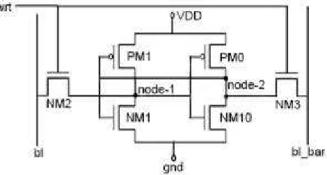
The conventional 6T SRAM cell consists of two cross -coupled inverters as illustrated in Fig.1. These cross coupled inverters PM0-NM0 and PM1-NM1, are used to store the data and ensure that the internal nodes of the cell always contain complementary values. Transistors NM2 and NM3 are the pass-gate transistors used to access the internal nodes.
Available online: https://edupediapublications.org/journals/index.php/IJR/ P a g e | 1903
For read operation, bitlines are precharged and wordline is given high voltage. The internal node storing logical zero will discharge its corresponding bitline via access transistor. Depending on whether the bitline is still charged or has been discharged, logical high and low of the cell is resolved. To write, the bitlines are given complementary values and then wordline voltage is raised. The corresponding node whose bitline is storing zero will be discharged via pass-transistor. In idle state, wordline is not asserted and hence internal nodes are disconnected from the respective bitlines. The cross-coupled inverters will continue to reinforce each other as long as power is being supplied to the cell.
III. PROPOSED DESIGN
The proposed SRAM cell is depicted in Fig 2. There is one PMOS transistor (PM0) at left node while the inverter on the right side is appended with a series connected NMOS transistor, NM1 (henceforth called the tail transistor). This tail transistor aids in reducing the short circuit power dissipation. Additional signal ‘cs’, is provided to control the tail device. The conventional 6T structure has two transistors to access the internal nodes while the proposed design has one access transistor i.e. NM2, to give write access while the other one, NM3 to give read access.
Figure 2. Proposed 6T SRAM cell.
The widths of pull-up and pull-down devices are 120nm and 220nm respectively and that of access transistors is 180nm for all the cells. For fair comparison, the width of tail transistor (NM1) is kept 120nm (minimum width). The length of all the
devices is 45nm. Hence, the β-ratio (WDriver/WAcess) equals
1.22 while the γ-ratio (WPull-Up/WAcess) equals 0.67. β-ratio
of 1.2-3.0 is required to avoid the read upset in conventional 6T SRAM cell while a γ-ratio ≤ 1.8 is required to maintain good write-ability [3,5].
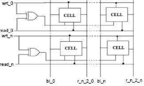
The distinct part of the proposed design is the series connected tail transistor. The ‘cs’ signal given to this tail transistor is the exclusive or (XOR) output of ‘wrt’ and ‘read’. The XOR gate serves the whole row as shown in Fig.3. The array structure of the proposed cell is shown in Fig.3.
Figure 3. Array of Proposed 6T SRAM cell.
The working of the proposed cell can be divided into three parts namely hold, read and write operations. These operations are explained as follows:
A. Hold Operation
For hold state, read and wrt are kept low. If n_1 is holding ‘0’, then NM0 would be off and PM1 would be on and hence n_2 will be connected to logic high. This in turn would turn off PM0 which cuts off n_1 from VDD, hence a zero is maintained at n_1. Similar is the case for holding ‘1’.
B. Read Operation
In the standard operation, bitlines are precharged and then the read is given high. During the read operation, the internal voltage of node storing zero rises which may result in flipping off contents of the cell. Hence data gets corrupted. In the proposed structure this case is not possible. Apart from this, the voltage of the bitline will not affect the internal node during read as separate port is provided for read operation (single ended read). The bitline is cut-off from the internal node being accessed. Hence, the data being read does not gets corrupted.
The bl is precharged and wrt is not asserted. Read is given high which gives the data stored in n_2 at r_n_2. C. Write Operation
Write operation for the proposed cell is same as that of standard 6T cell only with one difference that in the proposed structure only one bitline is precharged to high or low value. If ‘1’ is to be written, bl is charged and then wrt is turned on. Due to this NM0 turns on, which in turn drains down the voltage at n_2(if any). Hence, ‘0’ is written to n_2, which subsequently turns on PM0 and in turn connects n_1 to logic high. Hence, ‘1’ gets written to n_1. Likewise ‘0’ can also be written to n_1.
IV. SIMULATION RESULTS
Available online: https://edupediapublications.org/journals/index.php/IJR/ P a g e | 1904
variations have also come up as one of the major challenges. In the presence of process, voltage and temperature variations, this work aims at minimizing the power being dissipated.
A. Simulation Setup
The expected variations in supply voltage for technologies like 45nm as predicted by ITRS (2009) will be ±10%. The channel length (L), channel doping
concentration (NDEP), oxide thickness (tox) and threshold
voltage (Vt) are assumed to have independent Gaussian
distributions with a 3σ variation of 10% [6].
The present section compares the proposed design with standard 6T and LP10T cells on various performance metrics using Monte Carlo analysis. The analysis is done by changing supply voltage (0.8) by 10% of its nominal value.
TABLE I. WRITE DELAY COMPARISON AND ITS VARIABILITY
STD. Supply
SRAM
MEAN of TWA(s) Variability Voltage DEV. of
Cell
(mV) TWA(s)
Standard
4.0e-12 1.29e-1 1 0.31 0.88
4.2e-12 1.35e-11 (1) 0.31 (1) 0.80
6T 4.5e-12 1.45e-1 1 0.31 0.72
3.9e-12 1.25e-1 1 0.31 0.88
LP10T
4.0e-12 1.29e-11 (0.96) 0.31 (1) 0.80
4.2e-12 1.35e-1 1 0.31 0.72
Proposed
4.1e-12 1.32e-1 1 0.31 0.88
4.3e-12 1.34e-11 (1) 0.31 (1) 0.80
Cell
4.4e-12 1.37e-1 1 0.32 0.72
B. Write Access Time and its Variability
Write access time or write delay to write ‘1’ into the node storing ‘0’ is the time consumed from the instant when wrt is set high to the time when node storing ‘0’ rises to 90% of its full swing. In the same way, write delay to write ‘0’ into a node initially holding ‘1’ is the time elapsed from the instant when wrt is set high to the time when the node storing ‘1’ falls by 90% of its full swing. This ensures faithful write. Write delays are incurred mainly due to the PMOS transistors and the pass-gate devices. From Table I, it can be inferred that there is a negligible write delay (4%) in case of LP10T when compared to the delay incurred by standard 6T and our cell. Variability is calculated as the ratio of standard deviation to mean [1]. No improvement in variability has been observed.
C. Read Delay and its Variability
Read access time or read delay is estimated from the time when ‘wrt’ is activated to the time when bitline (bl) is discharged by 50mV from its initial high level [7]. As can be inferred from Table II, the proposed cell faces 7 %
additional delay as compared to standard 6T while LP10T faces 21% additional delay as compared to our cell.
As explained in section II, for standard 6T, after activation of ‘read’, ‘bl_bar’ discharges via transistors NM3/NM0 (assuming node_2 is storing ‘0’ and hence NM0 is in on state). Here, node_2 is initially grounded but at read point it elevates to 100mV due to the voltage dividing effect.
For the case of LP10T cell, both the nodes node_1 and node_2 are isolated by deactivating ‘wrt’. Assuming that node_2 is holding ‘0’, NM4 turns on while NM6 is off. This in turn elevates the node voltage at ‘Y’. Simulation results show that voltage at Y surges to 616mV and then drops down to 72mV at read point. Because of the presence
of positive voltage at Y, VbsNM4 (body to source voltage)
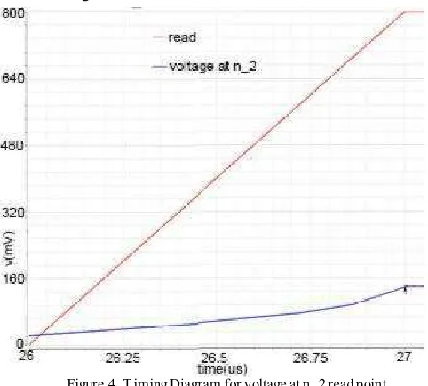
turns negative, thus increasing its threshold voltage and causes read delay. However, in the proposed cell, assuming n_2 is holding ‘0’, so NM0 is on. ‘r_n_2’ will discharge via NM3/ NM0/NM1. The voltage at n_2 rises to 137mV at read point. This can be seen in the timing diagram for n_2 shown in Fig.4.
Figure 4. T iming Diagram for voltage at n_2 read point.
TABLE II. READ DELAY COMPARISON AND ITS VARIABILITY
SRAM ST D. DEV. MEAN of Supply
Variability
Cell of TRA(s) TRA(s) Voltage
Standard 3.0e- 12 7.9e- 12 0.39 0.88
3.6e- 12 9.5e- 12 0.38 (1) 0.80
6T
3.7e- 12 9.8e- 12 0.38 0.72
4.1e- 12 1.02e - 0.40 0.88
LP10T
5.0e- 12 1.28e- 0.39 (1.02 ) 0.80
7.8e- 12 2.0e- 11 0.39 0.72
Proposed 3.3e- 12 8.5e- 12 0.38 0.88
3.91e-1 2 1.02e - 0.38 (1) 0.80
Cell
4.31e-1 2 1.06e - 0.40 0.72
Available online: https://edupediapublications.org/journals/index.php/IJR/ P a g e | 1905
D. Write- Ability
Write ability of the cell is the capability of the pass -gate device along with the write driver to flip the data which the cell is holding to, against the pull-up device which tries to restore its present state. If the pull-up device succeeds in its task, then write failure occurs. To avoid this condition, γ-ratio is carefully chosen.
Write static noise margin (WSNM) describes the capability of the cell to bring down the voltage of node holding ‘1’ below the switching voltage of the other inverter holding ‘0’, so that the contents stored in the cell can be flipped.
To calculate WSNM, wrt is asserted. Read and write voltage transfer curves are used to pictorially depict the write ability. For writing ‘1’ to n_1, write VTC is calculated by sweeping voltage at n_1 and monitoring voltage at n_2. Read VTC is calculated by sweeping voltage at n_2 and monitoring the variations in the voltage of n_1. These two graphs are plotted together and the smallest square that can be inscribed between them at the lower half represents WSNM.
As can be seen from Fig. 5, standard 6T, LP10T and the proposed cell show 200mV, 120mV and 205mV WSNM respectively. The proposed cell shows 1.025X and 1.7X higher WSNM as compared to standard 6T and LP10T cells respectively.
Figure 5. Combined WSNMs of all the cells.
propagation delays in the decoder circuit and wordline [9]. The operating frequencies of standard 6T, LP10T and the proposed cell are illustrated in Table III. Our cell has its operating frequency comparable to the standard cell and higher than the LP10T cell.
TABLE III. COMPARISON OF OPERATING FREQUENCIES OF THE CELLS.
SRAM Cell Operating Frequency(MHz) Supply Voltage (mV)
466.67 0.72
Standard 6T 527.19 0.80
600.33 0.88
317.98 0.72
LP10T 398.23 0.80
478.13 0.88
445.8 0.72
Proposed Cell 500.17 0.80
589.11 0.88
G. Leakage Analysis
The leakage components increase at an alarming rate for short channel devices. The various components of leakage current are depicted in Fig.6. Gate drain leakage is further subdivided into gate drain overlap leakage and gate channel drain leakage. In the similar way gate source leakage is constituted. As already stated, the main constituents of leakage
current are ISUB, IG and IJN. The variation of leakage currents
for the minimum sized device with respect to temperature variation are plotted and shown in Fig. 7. As can be interpreted from the plot, it is subthreshold current which contributes
mainly towards leakage current and is ideally equal to ISUB.
ISUB varies from 5pA to 55pA while the IG varies from 79fA
to 136fA for a temperature range of 25ºC to 150ºC. From the
plot, it can be inferred that ISUB increases exponentially with
the increase in temperature due to its dependence on VT (=
kT/q).
I I e /
1 e
/ (1)
E. Read Stability
RSNM is calculated pictorially by measuring the length of the largest square that can be inscribed inside the smallest lobe of the butterfly curve. The RSNM of proposed cell shows slightly less stability as compared to standard 6T and LP10T cells due to its non-symmetric structure.
F. Operating Frequency
Operating frequency is the inverse of a cycle time,
Available online: https://edupediapublications.org/journals/index.php/IJR/ P a g e | 1906 Figure 7. Variation of Leakage Current components with Temperature.
IJN also increases with temperature due to an increase
in the number of minority carriers. IJN has not been shown
in the plot due to its very small value as compared to the other two components. The leakage current for the proposed cell is very less in comparison to the LP10T as can be seen from Fig. 8 in [1].
H. Power Dissipation
Mostly the cache remains in its standby mode and this necessitates the need for minimizing power dissipation in hold mode. The major contributors towards leakage power in hold mode are derived from leakage current expressions.
Major leakage current components for standard 6T cell in hold mode are as follows:
Isub = IsubNM2 +IsubNM0 + IsubPM1
IJN = IJNsNM3 +IJNdNM3 + IJNdNM2 + IJNdNM0 +IJNdPM1
IG = IGdNM3 +IGsNM3 + I GdNM2 + IGdPM1+IGdNM1 +IGsNM1
+IGdPM0 + IGsPM0 + IGdNM0
Major leakage current components for LP10T cell in hold mode are as follows:
Isub = IsubNM1 +IsubNM2 + IsubNM4 +IsubNM5 + IsubNM6 +IsubNM7
+IsubNM9 + IsubPM2
IJN = IJNsNM10+IJNdNM10+ IJNdNM2 + IJNsNM9+ IJNdNM1 +
IJNsNM1 + IJNdPM2 + IJNdNM5 + IJNdNM4 +IJNsNM4 +
IJNdNM6 + IJNsNM6 +IJNdNM7
IG = IGdNM10 + IGsNM10 + IGdNM2 + IGdPM2 + IGdNM9 + IGsNM9
+ IGdPM1 + IGsPM1+ IGdNM1 +IGsNM1 +IGdPM4 + IGdNM5
+ IGsNM4 + IGsNM6 + IGdNM7
Major leakage current components for the proposed cell in hold mode are as follows:
Isub = IsubNM3+IsubNM0 + IsubPM1
IJN = IJNdNM3 +IJNsNM2+ IJNdNM2 + IJNsNM0 +IJNdPM1+ IJNdNM1
IG = IGdNM2 + IGsNM2 + IGdPM1 + IGdNM0 + IGsNM0 + IGdPM0 +
IGsPM0 + IGdPM1
In the conventional structure (Fig.1), the source of pull-down transistor is connected to ground while in the proposed design it is connected to transistor NM1. This provides the stacking effect. The node between NM1 and NM0 is termed as ‘Y’. Assuming ‘1’ stored in n_2, the voltage at node Y therefore increases. This positive voltage at node Y (around 150mV) provides the stacking effect. This stacking effect provided by NM0 and NM1 results in
negative Vgs, negative Vbs and reduction in Vds. Due to the
changes in the above stated voltages, the sub-threshold current reduces according to Eq 1.
The impact of VY can be explained as follows:
Due to positive VY, gate to source voltage of NM0
becomes negative and hence lowering subthreshold leakage current to some extent.
Due to positive VY, body to source voltage of NM0
turns negative which in turn increases threshold voltage and hence curtails subthreshold leakage.
Again due to positive VY, the drain to source
voltage of NM0 decreases which in turn will result in increase in threshold voltage and thus reducing subthreshold leakage.
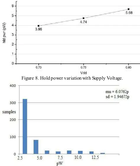
In idle mode, sub-threshold current is mainly responsible for the leakage and in the proposed design it is being lowered down due to the stacking effect. The proposed design gives very low power dissipation (4.74154pW) during idle mode and it curtails the short circuit power dissipation as during transition phase as there is no direct path from supply voltage to ground. The variation of hold power with the change in supply voltage is shown in Fig. 8.
Figure 8. Hold power variation with Supply Voltage.
Available online: https://edupediapublications.org/journals/index.php/IJR/ P a g e | 1907
I. Corner Analysis V. CONCLUSION
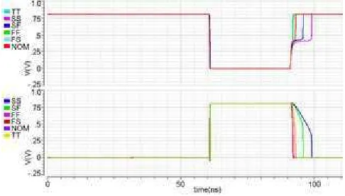
The corner analysis for the proposed design is also carried out. For the worst corner SF (Slow NMOS- Fast PMOS), the variations in voltage at n_1 for hold ‘1’ and ‘0’ states are shown in Fig.10 and Fig.11 respectively. Corner analysis for all process corners i.e. FF, FS, SF, SS and TT, for writing ‘1’ to n_1 and ‘0’ to n_2 is also illustrated in Fig.12.
Figure 10. Worst case(SF) corner analysis of voltage at n_1 for hold 1
This paper presents an SRAM cell with very low power dissipation for standby mode. The effect of PVT variations on the performance metrics of the proposed cell is studied. Keeping all constraints in mind, it can be concluded that the proposed SRAM cell is a good contender for low power applications in nanometer regime.
REFERENCES
[1] A. Islam and M. Hasan, “Leakage Characterization of 10T SRAM Cell”, IEEE T ransactions on Electron Devices, Vol. 59, No. 3, March 2012.
[2] Y. Y. Wang, Z.O. Wang, L.J. Zhang, “A New 6-T ransistor SRAM Cell for Low Power Cache Design”, IEEE Conf. on Solid State and Integrated Circuit T echnology, Oct., 2012, pp. 1-3.
[3] N. Verma, J. Kong and A. P. Chandrakasan, “Nanometer MOSFET variation in minimum energy suthreshold circuits,” IEEE T rans. Electronic Devices, Vol. 55, pp. 163-174, Jan. 2008.
[4] Z. Liu and V. Kursun, “Characterisation of a novel nine transistor SRAM cell,” IEEE T rans. VLSI Syst., Vol. 16, no. 4, pp. 488-492, April 2008.
[5] J. M. Rabaey, A. Chandrakasan, and B. Nikolic, in Digital Integrated Circuits: A Design Perspective, 2nd ed. New Delhi, India: Prentice-Hall, 2005.
[6] R. Vaddi, S. Dasgupta, and R. P. Agarwal, “Device and circuit co- design robustness studies in the subthreshold logic for ultralow-power applica- tions for 32 nm CMOS,” IEEE T rans. Electron Devices, vol. 57, no. 3, pp. 654–664, Mar. 2010.
[7] J. P. Kulkarni, K. Kim, and K. Roy, “A 160 mV robust Schmitt trigger based subthreshold SRAM,” IEEE J. Solid-State Circuits, vol. 42, no. 10, pp. 2303–2313, Oct. 2007.
[8] M. Mamidipaka et.al “Leakage Power Estimation in SRAMs,” Motorola Co., USA, Sept. 2003.
[9] H. Noguchi et al “Which is the best dual-port SRAM in 45-nm process technology?—8T, 10T single end, and 10T differential,” IEEE Proc. ICICDT, Jun. 2008, pp. 55–58.
Figure 11. Worst case(SF) corner analysis of voltage at n_1 for hold 0