ABSTRACT: This paper proposes power conditioning scheme based on fuzzy logic for load side inverter. In this configuration a single-phase transformer less inverter for grid-tied photovoltaic (PV) system because of minimal effort, high efficiency, light weight, and so forth. In this way, numerous transformer less topologies have been proposed and confirmed with genuine power infusion as it were. As of late, practically every worldwide control has forced that an unequivocal measure of reactive power ought to be taken care of by the grid-tied PV inverter The new topology structure and detail operation principle with reactive power flow is portrayed. The high frequency common mode (CM) model and the control of the proposed topology are broke down. The inalienable circuit structure of the proposed topology does not lead itself to the turnaround recuperation issues notwithstanding when infuse reactive power which permit using MOSFET changes to support the general efficiency. The CM voltage is kept consistent at midpoint of dc input voltage, comes about low spillage current. There has been an expanding enthusiasm for transformer less inverter for grid-tied photovoltaic (PV) system because of ease.
Index Terms—Bipolar voltage multiplier (BVM), hybrid boosting converter (HBC), nature interleaving, renewable energy, singleswitch single inductor.
1. INTRODUCTION
Recently , the photovoltaic power era system has been engaged as a standout amongst the most noteworthy energy sources because of the rising worry about an Earth-wide temperature boost, and the expansion of electrical power utilization. What's more, the PV module has no moving parts, which have made it extremely powerful, long lifetime and low upkeep gadget. Despite the fact that the PV module is as yet costly, however because of the huge scale manufacturing it has turned out to be progressively less expensive over the most recent couple of years. It has been accounted for in that the point of reference of 100GW introduced PV power everywhere throughout the world was achieved toward the finish of 2012 and expanded to 140GW toward the finish of 2013, and the larger part were grid associated. Consequently, an expectation has been made in that the future grid tied PV system will assume an imperative part in the direction of the conventional power system.
II.STRUCTURE OF PROPOSED TOPOLOGY
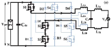
Fig. 1 shows the proposed transformer less inverter topologies consisting of six MOSFET switches (S1-S6) and six diodes (D1-D6). L1A, L1B, L2A, L2B, L1g, L2g and Co make up the LCL type filter connected to the grid. VPV and Cdc represent the input dc voltage and dc link capacitor. Therefore, the proposed topology can be implemented with MOSFET switches without reliability and efficiency penalty. The proposed topology can also employ unipolar-SPWM with three-level output voltage.
Fig 1Circuit structure of the proposed transformerless topology for gridtied PV system
III.OPERATING PRINCIPLE OF THE
PROPOSED TOPOLOGY
Fig 2 Switching pattern of the proposed topology with reactive power flow
Region I:
In this locale, both the grid current and voltage are certain. Amid the period inside this district, S2 is dependably on, while S1 and S3 synchronously and S5 reciprocal commutate with switching frequency. here are constantly two expresses that produce the output voltage of +VPV and 0.
State 1(t0:t1):
At t = t0, the switches S1 & S3 are turned on and the inductor current increases through grid as shown in Fig. 6(a). In this state, the voltages V1N and V2N can be defined as: V1N = +VPV and V2N = 0, thus the inverter output voltage V12 = (V1N − V2N) = +VPV .
Fig. 3 The operating principle of the proposed topology: state 1
State 2(t1:t2):
When the switches S1 and S3 are turned-off, the inductor current freewheels through S2 and D5. In this state, V1N falls and V2N rises until their values are equal. Therefore, the voltages V1N and V2N becomes: V1N = VPV /2 and V2N = VPV /2 and the inverter output voltage V12 = 0.
Fig 4 The operating principle of the proposed topology: state 2 .
Region II:
In this region, the inverter output voltage is negative, but the current remains positive. During the period of this region, S5 is always on, while S4 & S6 synchronously and S2 complementary commutate with switching frequency. There are also two states that generate the output voltage of −VPV and 0.
Fig 5 The operating principle of the proposed topology: state 3
State 3(t3:t4):
In this state, the switches S4 and S6 are turned-on and the filter inductors are demagnetized. Since the inverter output voltage is negative and the current remains positive; therefore, the inductor current is forced to freewheel through the diode D1 and D2, and decreases rapidly for enduring the reverse voltage as shown in Fig. 5(c). The voltages V1N and V2N can be defined as: V1N = 0 and V2N = +VPV , thus the inverter output voltage V12 = (V1N - V2N) = -VPV .
Fig 6 The operating principle of the proposed topology: state 5
State 4(t4:t5):
Fig 7 The operating principle of the proposed topology: state 6
IV. FUZZY LOGIC
In recent years, the number and variety of applications of fuzzy logic have increased significantly. The applications range from consumer products such as cameras, camcorders, washing machines, and microwave ovens to industrial process control, medical instrumentation, decision-support systems, and portfolio selection. To understand why use of fuzzy logic has grown, you must first understand what is meant by fuzzy logic.
Fig.8 The Primary GUI Tools Of The Fuzzy Logic Toolbox
The FIS Editor handles the high level issues for the system How much input and output variables? What are their names? The Fuzzy Logic Toolbox doesn't limit the number of inputs. However, the number of inputs may be limited by the available memory of our machine. If the number of inputs is too large, or the number of membership functions is too big, then it may also be difficult to analyse the FIS using the other GUI tools. The Membership Function Editor is used to define the shapes of all the membership functions associated with each variable. The Rule Editor is for editing the list of rules that defines the behaviour of the system.
4.1The FIS Editor
The following discussion walks we through building a new fuzzy inference system from scratch. If we want to
Fig.9 The FIS Editor
We will see the diagram updated to reflect the new names of the input and output variables. There is now a new variable in the workspace called tipper that contains all the information about this system.
Fig.10 „Save to workspace as...‟ window By saving to the workspace with a new name, we also rename the entire system. Our window will look like as shown in Fig.9.
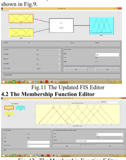
Fig.11 The Updated FIS Editor 4.2 The Membership Function Editor
Fig.13 Add MFs… Window
Fig.14 The Updated Membership Function Editor 4.3 The Rule Editor
Fig.15 The Rule Editor
Fig.16 Fuzzy rules
V. SIMULATION RESULTS
In order to verify the feasibility of proposing converter and its performance, simulation results of. Fig.17. shows Simulink model of proposed converter.
Fig 17 simulink model of proposed system
Fig 18 CM characteristics of the proposed topology with
real and reactive power flow.(V1N&2N)
Fig 19 CM characteristics of the proposed topology with pure real power flow
VI.CONCLUSION
PWM dead time is not required for the proposed topology that reduces the THD at the output.
REFERENCES
[1] W. Chen, A. Q. Huang, C. Li, G. Wang, and W. Gu, “Analysis and comparison of medium voltage high power DC/DC converters for offshore wind energy systems,” IEEE Trans. Power Electron., vol. 28, no. 4,pp. 2014–2023, Apr. 2013.
[2] J. A. Starzyk, “A DC-DC charge pump design based on voltage doublers,”IEEE Trans. Circuits Syst. I Fundam.. Theory Appl., vol. 48, no. 3,pp. 350–359, Mar. 2001.
[3] N. Vazquez, L. Estrada, C. Hernandez, and E. Rodriguez, “The tappedinductor boost converter,” in Proc. IEEE Int. Symp. Ind. Electron.,Jun. 2007, pp. 538–543.
[4] R. Wai, C. Lin, R. Duan, and Y. Chang, “High-efficiency DC-DC converter with high voltage gain and reduced switch stress,” IEEE Trans. Ind.Electron., vol. 54, no. 1, pp. 354–364, Feb. 2007.
[5] A. Lamantia, P. G. Maranesi, and L. Radrizzani, “Small-signal model of the Cockcroft-Walton voltage multiplier,” IEEE Trans. Power Electron.,vol. 9, no. 1, pp. 18–25, Jan. 1994.
[6] K.-C. Tseng, C.-C.Huang, and W.-Y.Shih, “A high step-up converter with a voltage multiplier module for a photovoltaic system,” IEEE Trans.Power Electron., vol. 28, no. 6, pp. 3047–3057, Jun. 2013.
[7] B. Axelrod, G. Golan, Y. Berkovich, and A. Shenkman, “Diode–capacitor voltage multipliers combined with boost-converters: Topologies and characteristics,”IET Power Electron., vol. 5, no. 6, pp. 873–884, Jul. 2012.
[8] F. L. Luo, S. Member, and H. Ye, “Positive output super-lift converters,”IEEE Trans. Power Electron., vol. 18, no. 1, pp. 105–113, Jan. 2003.