Design of a Low Loss Silicon Based Hybrid Dielectric-Loaded
Plasmonic Waveguide and a Compact High
Performance Optical Resonator
Cheng-Hung Hsieh, Yu-Ting Chu, Min-Jyun Huang, Chien-Ming Kuo, and Keh-Chyang Leou*
Abstract—Here we present the design of a low loss top metal silicon (Si) hybrid dielectric-loaded plasmonic waveguide (TM-SiHDLW) and a compact, high performance optical resonator by numerical simulation based on finite element method. The waveguide adopted a thick (200 nm) top metal stripe structure to yield optimal performance due to reduced Ohmic loss in conductor around the stripe edge/corner. Moreover, a relatively thick (150 nm) dielectric spacer between the Si ridge and the metal stripe was employed to achieve both long propagation length and good field confinement. The effect of a thin (10 nm) silicon nitride (SiNx) layer covering the waveguide which was added for minimizing uncertainties on optical properties of SiHDLW resulting from high density of dangling bonds on Si surface was also investigated. Simulation results show that there is no significant degradation on the performance of the TM-SiHDLW. For the proposed plasmonic waveguide, a propagation length of 0.35 mm and a mode area around 0.029µm2 were demonstrated. The TM-SiHDLW waveguide was then used as the basis for an optical resonator, which was designed to operate at the fundamental TE011
mode for yielding high quality factor at a relatively small footprint size. A metal enclosure was also adopted to reduce the radiation loss, and a high quality factor of∼1900 was obtained, more than double the results in other disk or ring resonators of comparable size. Compared to the resonators based on a rounded top metal Si hybrid dielectric-loaded plasmonic waveguide (RTM-SiHDLW) which has a much longer propagation length than the TM-SiHDLW, as reported in our previous work, the performance is essentially the same. This is simply because, for the resonators, the radiation loss is the dominate loss mechanism and the dissipation in the waveguide structure itself, thus, contribute little to the final quality factor of the plasmonic resonators.
1. INTRODUCTION
Recently, many applications related to collective electronic excitations (plasmons) have emerged, giving rise to new research fields of plasmonics [1–5]. Lately, surface plasmon polariton waveguides (SPPWGs) have attracted a great deal of attention as promising means for information transmission at nano scale due to strong local confinement of electromagnetic (EM) energy on sub-wavelength scale [6]. The optical properties of the SPPWGs are often characterized by two fundamental parameters, propagation length (Lprop) and field confinement (mode area, Am). For application of SPPWG in integrated optics, it is
highly desirable to develop a SPPWG with long propagation length while still having small mode area. However, a trade-off between the two fundamental parameters in SPPWGs has been the major challenge of SPPWG design [7, 8]. Among varieties of SPPWGs, the hybrid dielectric-loaded (DL) SPPWG
Received 28 April 2015, Accepted 4 June 2015, Scheduled 16 June 2015
* Corresponding author: Keh-Chyang Leou (kcleou@ess.nthu.edu.tw).
combines the advantages of hybrid SPPWG [9–11] and DL SPPWG [12]: Long propagation length, relatively small mode area, and nanometer dimension of SPPWG [13–15]. The hybrid DL SPPWG using silicon (Si) dielectric (Si-based hybrid DL SPPWG, SiHDLW) [7, 8, 10, 13, 14, 16–18], which has been shown to yield strong field confinement [8, 10, 13, 17, 18], is a particularly attractive candidate for plasmonic devices because the waveguide is easier to fabricate with conventional nano/micro techniques [7]. In addition, SiHDLW optical devices adopting Silicon-on-Insulator (SOI) substrate, such as splitters [7], couplers [7, 19], and modulators [20] have also been demonstrated. Furthermore, the SiHDLW shows two common structures of top metal SiHDLW (TM-SiHDLW) [7, 8, 16, 17, 21] and bottom metal SiHDLW (BM-SiHDLW) [10, 14, 22]. The TM-SiHDLW shows a more promising potential than the BM-SiHDLW because of its flexibility to integrate with nanophotonic circuits [18]. For the SiHDLWs, a mode area as low as 0.0007µm2–0.018µm2 has been achieved but with a propagation length limited in the range of 20µm–100µm [8, 16–18]. A special design running at a high order SPP waveguide mode have been proposed to give a propagation length as high as 1 mm but with a large mode area of 0.15µm2, as expected [18]. In addition, it might not be as easy to excite a high order waveguide mode efficiently. A TM-SiHDLW with a thin alumina dielectric spacer has been analyzed [21]. But the waveguide is still quite lossy due to the high refraction index of alumina [21]. Accordingly, a SPPWG with long propagation length would provide a much greater flexibility in the design of components of the SPPWG optical circuits. On the other hand, one should note that although these studies have achieved very small mode area, the physical size are quite large, e.g., cross section areas ≥ 200 nm ×500 nm, or SPPWG width ≥ 200 nm. The density of the nano photonic circuits will be limited by these physical sizes, instead of the mode areas. To improve the feasibility of adopting SiHDLWs in integration circuits, the major challenge is to increase the propagation length. Therefore, in this study, the dimensions of a TM-SiHDLW are optimized according to parameters, such as propagation length, mode area, and EM field distribution of the hybrid SPP mode. For conventional TM-SiHDLWs, the Si dielectric ridge is often exposed to air [10, 23]. The property of the hybrid DL SPPWG might become unpredictable due to the formation of native oxide whose thickness may vary significantly due to environmental conditions [24, 25]. Hence, after the optimized size of the TM-SiHDLW, an effect of a SiNx cladding layer covering the SPPWG for better control of optical properties of the waveguide is determined. Finally, a disk optical resonator based on the TM-SiHDLW we presented is designed, and the effect of metal enclosure is also analyzed.
2. DESIGN AND ANALYSIS OF TM-SIHDLW
For the design and analysis of the TM-SiHDLW, numerical simulation was performed by using a finite element code, COMSOL Multiphysics. For a given waveguide cross section structure, eigenmodes corresponding to the desired free space wavelength, 1.55µm, were solved, yielding the complex refractive index (n) of the SPP mode,n=neff +iκ, whereneff is the effective refractive index andκcorresponds
to waveguide loss. The effective refractive index (neff), related to the propagation constant of the hybrid
mode by neff =k/k0 wherek0 being the free space wave number. For a hybrid SPPWG consisting of
regions with dielectrics of different values of index refraction is also an indicator where the wave power propagates. A higherneff means a higher fraction of wave power propagating in the region of high index
of refraction. The propagation length (Lprop) is given by [9]
Lprop = 1/2β0κ, (1)
whereβ0 is the propagation constant for plane wave in vacuum.
The mode area (Am), a measurement of field confinement, is defined as [9]:
Am=
∞W
rdA/maxWr, (2)
whereW(r) is the energy density, given by
W r= 1/2
Reεr Er2+μ0H
r2 , (3)
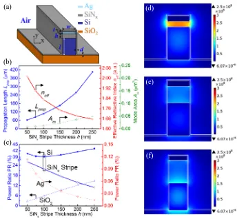
The cross section of the TM-SiHDLW consisting of a rectangular Si, SiNx stripe and silver (Ag) film on a SiO2 substrate is shown in Figure 1(a). The corresponding relative permittivities of Si, SiNx,
SiO2, and Ag used in the simulation are 12.11, 2.0, 2.08 and−129.005 +i3.294 [26], respectively.
In previous studies of hybrid DL SPPWG [7, 8, 17], the effect of waveguide width has been investigated. Both Lprop and Am were found to increase with waveguide width. Here we show that
a longer Lprop and smaller Am can be achieved by optimizing the thickness of sandwiched dielectric
stripe, waveguide width and metal thickness. Furthermore, the effect of thickness of a SiNx cladding layer is also investigated.
3. SIMULATION RESULTS AND DISCUSSIONS
We first consider a typical TM-SiHDLW, as depicted in Figure 1(a), and examine the effect of waveguide width, w. The resulting propagation length (Lprop), effective refractive index (neff), and mode area
(Am) are shown in Figure 1(b). Figure 1(c) shows the power ratio (PR) in different materials of the waveguide. The PR is defined as the ratio of power in a material to total power in overall waveguide where the power is determined by integrating the Poynting vector over cross section area of the region under consideration. Figures 1(d)–(f) illustrate the distribution of E field strength for different values of w. As have been shown in previous study [3], all three waveguide properties increase with w. For w= 0.5µm, one obtains aLprop of nearly 0.57 mm butAm also rises to∼0.18µm2. Whenw increases,
as shown in Figure 1(c), the PRSi rises while both PRAg and PRSiNx Stripe drop, indicating that more
power concentrates into Si, resulting in the increase of both neff and Am with w accordingly. The E
field strength profiles of Figures 1(d)–(f) also demonstrate that the field penetrates more into Si as w
(a)
(b)
(c)
(d)
(e)
(f)
Figure 1. (a) Cross section of typical TM-SiHDLW. (b) Dependence of Lprop, Am, and neff on w.
(c) PR of Si, Ag, SiO2, and SiNx stripe. Distribution of E field strength in typical TM-SiHDLW:
increases. To maintain a small mode area, e.g., Am <0.03µm2, a relatively narrow waveguide width, i.e., w∼200 nm, would be required, according to the results in Figure 1(b), but the correspondingLprop
drops to∼0.115 mm. We will show that by optimizing two other parameters, SiNx stripe thickness (h) and metal height (t), one can increase the propagation length toLprop∼0.35 mm while still keepingAm
around 0.03µm2.
As mentioned earlier, a thin (10 nm) SiNx cladding layer (d = 10 nm) covering the TM-SiHDLW will be included for the SPPWGs in the following analysis, as depicted in Figure 2(a). We will also show later that a 10 nm SiNx cladding layer only affects the property of the SPPWG slightly. First, the simulation results for the effect of h are shown in Figure 2(b). As expected, theLprop increases with h
while correspondingneff decreases. This can be explained by examining the PR in different materials of
the waveguide, as shown in Figure 2(c). From Figure 2(c), ash increases, PRSirises while PRAg drops accordingly, indicating that the power loss in Ag would decrease, and the resulting Lprop increases.
Moreover, the increasing of PRSiO2 withhmeans that more power concentrates in SiO2 areas, resulting
in the falling neff. Although theLprop increases withh,Am also increases accordingly. Ash decreases,
the energy more focuses into SiNx stripe, leading to a well field confinement (the decreasing ofAm) and thus a shortLprop and vice versa. As an example, we show the strength of E field forh= 50, 150, and
250 nm in Figures 2(d)–(f). One can clearly see that the best strength confinement of E field in SiNx stripe is in the case of h = 50 nm while the case of h = 250 nm exhibits the weakest confinement. To maintain a small mode area (Am <0.03µm2) and also balance the trade-off between Lprop and Am, a
150 nm-thick SiNx stripe is adopted for further optimization of the TM-SiHDLW so that a good field confinement is maintained for the hybrid SPP mode.
(a)
(b)
(c)
(d)
(e)
(f)
Figure 2. (a) Cross section of TM-SiHDLW with a SiNx cladding layer. (b) Dependence ofLprop,Am,
and neff on h. (c) PR of Si, Ag, SiO2 substrate and SiNx stripe. Distribution of E field strength of
(a)
(b)
(c)
(d)
(e)
(f)
Figure 3. (a) Dependence of Lprop, neff and Am on t. PR of (b) Ag, Si, and (c) SiNx stripe, and
SiNx cladding layer. Distribution of E field strength of the designed TM-SiHDLW: (d) t = 50 nm, (e)t= 200 nm, and (f)t= 500 nm, where w= 200 nm, h= 150 nm, l= 300 nm, andd= 10 nm.
Next, we examined the effect of metal height (t), and the results are illustrated in Figure 3(a). The dependence of PR in different materials is shown in Figures 3(b)–(d). From Figure 3(a),Lprop increases
withtsince the corresponding power, and hence the loss, in Ag film drops as shown in Figure 3(b). The variation of neff is less than 0.9% as t increases from 50 nm to 500 nm, also consistent with the results
that PRSi, PRSiNx Stripe, and PRSiNx Cladding Layer only vary slightly (< 3%) in Figures 3(b) and (c).
In addition, the mode areas, Am, are kept in the range of 0.022µm2–0.029µm2. Also note thatLprop
only increases slightly for t > 200 nm (less than 7% as t increases from 200 nm to 500 nm), consistent with the results that PRAg also changes little, as depicted in Figure 3(b). To explain the trend ofLprop
against t, we show the profiles of E field strength for t = 50 nm, 200 nm and 500 nm, respectively, in Figures 3(d)–(f). For the case of t = 50 nm in Figure 3(d), the distribution of E field strength wraps around both bottom and top corners of the edges of the Ag film, in contrast to the other two cases. This can be attributed to that for thin Ag film, the EM energy spreads over the top corners of the Ag film. It is well known that field strengths are enhanced near sharp corners, and thus, as a result, a higher power loss for SPPWG. This is also consistent with the higher PRAg for t= 50 nm case as illustrated in Figure 3(b). On the other hand, also shown in Figures 3(d)–(f), ast increases, the E field strength penetrates more into Si instead of covering the top of Ag film. This is also consistent with the results in Figure 3(b) where PRAg drops while PRSi increases witht. It should be noted that from these results, there would be little benefit to have t > 200 nm. Therefore, for our optimized SPPWG, a 200 nm Ag height is chosen to yield longLprop and small Am.
Further, the effect of SiNx cladding layer thickness (d) on Lprop, neff, Am and PR is shown in
(a) (b)
Figure 4. (a) Dependence of Lprop, neff, and Am on d. (b) PR in Si, Ag, and SiNx cladding layer,
wherew= 200 nm,t= 200 nm,h= 150 nm, andl= 300 nm.
Figure 4(a) shows that the Lprop decreases with dwhile neff increases as a function of d. In addition,
the variation ofAmdue todis small, and theAmis in the range of 0.020µm2–0.034µm2. The increasing of PRAgwithd, as shown in Figure 4(b), indicates that more power consumption in Ag as SiNxcladding layer becomes thicker, leading to a decreasingLprop. Further, the PRSi, the major part of energy flux
in the waveguide, varies little with d (less than 1%), and, consequently, neff also only varies slightly
(<4.3%). Compared with the case without cladding layer (d= 0 nm), there is a minor drop (∼6.7%) of Lprop for the case of 10 nm-thick SiNx, as depicted in Figure 4(a), andAm varies only from 0.026µm2
to 0.029µm2. Therefore, for our proposed SPPWG, a 10 nm-thick SiNx cladding layer is adopted, and the resulting Lprop and Am are 350µm and 0.029µm2, respectively.
In this study, an optical resonator based on the proposed TM-SiHDLW has also been analyzed. There were two typical structures, i.e., ring resonator [27–30] and disk resonator [30–32], often adopted in the works reported previously. For the disk resonator, an unloaded quality factor (Q) of 920, operated at TM plasmonic mode and a high order azimuthal modem = 7, has been investigated at a resonator radius of 850 nm [30]. At slightly larger ring radius of 1000 nm, a Q up to ∼1000 has also been achieved [27]. For the disk resonator based on the designed TM-SiHDLW, as shown in Figure 5(a), we operated at the TE mode, often chosen for microwave dielectric resonators [33], and the characteristics of the TE011 mode disk resonator were also analyzed numerically using COMSOL Multiphysics. By
employing the symmetry property of the TE011 mode, only a quarter section of the resonator was
considered in the model, with boundary condition — perfect electrical wall, PEC, at the bisected cross section surfaces. The radius of the resonator was adjusted so that TE011 mode resonance occurs at a
frequency corresponding to the telecommunication wavelength, 1550 nm. For the disk resonator shown in Figure 5(a), based on the optimized waveguide design, i.e., l= 300 nm,h= 150 nm,t= 200 nm, and d= 10 nm, simulation analysis shows that for a disk radius (R) of 464 nm, the quality factor is about 22, typical for disk resonator as a result of high radiation loss due to their compact size. Figure 5(b) illustrates the top and cross sectional views of the E field strength distribution at resonance. Note that from the inset of Figure 5(b), the main radiation appears leaking through the lateral and bottom surface of the resonator.
(RTM-(a) (b)
Figure 5. (a) Configuration of a disk resonator based on TM-SiHDLW. (b) Top view of quarter section of normalizedE field strength distribution. The inset in (b) shows the half cross section of distribution. The dimension of resonator: R= 464 nm, and the others are the same as those shown in Figure 4 with d= 10 nm.
(a)
(b)
(c)
(d)
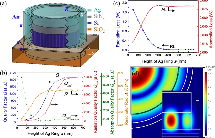
Figure 6. (a) Structure of a TM-SiHDLW-based disk resonator with 50 nm-thick Ag ring and bottom Ag plate. (b) Dependence of Qabs, Qrad, Q, and R on a. (c) Dependence of absorption loss and
radiation loss on a. (d) Top view of quarter section of normalized E field strength distribution. The inset in (d) shows the half cross section of distribution. Withg andbof 85 and 75 nm, respectively, the other dimensions of resonator, exceptR, are the same as those in Figure 5.
SiHDLW) proposed in our previous study [34]. Therefore, the resonator withg and b of 85 and 75 nm, respectively, was then used as the basic structure of TM-SiHDLW-based resonator. Then, we examined the effect of the Ag ring height (a) onQ, Qabs, Qrad, and R, as shown in Figure 6(b), where the disk
radius R was certainly adjusted so that the resonance occurred at the 1550 nm wavelength. The Q could be obtained by 1/Q = 1/Qabs + 1/Qrad where Qabs is related to the absorption loss and Qrad
Q varies little (variation of ∼1.0%) since the magnitude of radiation loss and absorption loss almost do not change with a as shown in Figure 6(c). From Figure 6(d), one could also confirm that the E field strength confines well inside the metal envelope, and so does the corresponding radiation loss. According to these results, a 500 nm-high Ag ring was adopted for our design of TM-SiHDLW-based optical disk resonator, yielding a Q ∼ 1900 at a resonator area (= π·(R+g+ 50 nm)2) ≈1.25µm2. As a result, compared with other plasmonic resonators in the previous studies [27–32], a quality factor of the proposed TM-SiHDLW-based resonator is almost twice the results of other resonators as keeping a comparable footprint. Therefore, the designed TM-SiHDLW is demonstrated to have an attractive potential as the basic structure for high performance optical disk resonator.
4. CONCLUSIONS
In this work, we have designed and characterized a top metal Si hybrid dielectric-loaded plasmonic waveguide (TM-SiHDLW), yielding both a long propagation length of 0.35 mm and a small mode area of 0.029µm2 at telecommunication wavelength. The propagation length was more than doubled by increasing the height of the top metal stripe from 50 nm to 200 nm to reduce the power loss in metal caused by enhancement effect of E fields near conductor sharp corners. To protect the SPPWG while avoiding significant reduction of its propagation length, a thin SiNx cladding layer has been added and the effect of its thickness has also been analyzed. For a SiNx cladding layer thickness of 10 nm, the propagation length was found to drop slightly (<7%) while mode area only increases from 0.026µm2 to 0.029µm2. The TM-SiHDLW with optimized dimensions was also used in the design of an optical disk resonator, operating at fundamental TE011 mode. From the simulation results, the radiation loss
was reduced by employing a metal envelope, containing a ring and bottom plate. A quality factor of ∼1900 with a relatively small size of 1.25µm2 has been achieved by employing a metal ring with∼3/4 height of the resonator. The performance of the TM-SiHDLW-based resonator is essentially comparable to that based on RTM-SiHDLW, reported in our previous work [34], which shows a longer propagation length than the proposed TM-SiHDLW. The cause is clearly that for the two resonators, the major loss mechanism comes from the radiation loss while only little contribution from the absorption of the waveguide structure itself to the final quality factor of the resonators. It might be worthy to explore fabricating the Si waveguide using hydrogenated amorphous Si (i.e., α-Si:H) deposited by plasma enhanced chemical vapor deposition process(PECVD) [35, 36] to increase the flexibility of the fabrication process of the TM-SiHDLW, as compared with the SOI wafer based process employed in previous works [7, 19, 20].
ACKNOWLEDGMENT
This work has been financially supported by the Ministry of Science and Technology (MOST) of Taiwan, R. O. C.. The authors especially thank the “National Center for High-Performance Computing” of Taiwan, R. O. C., for providing simulation code.
REFERENCES
1. Politano, A. and G. Chiarello, “The influence of electron confinement, quantum size effects, and film morphology on the dispersion and the damping of plasmonic modes in Ag and Au thin films,”
Prog. Surf. Sci., Vol. 90, No. 2, 144–193, May 2015.
2. Politano, A. and G. Chiarello, “Unravelling suitable graphene-metal contacts for graphene-based plasmonic devices,”Nanoscale, Vol. 5, No. 17, 8215–8220, Sep. 2013.
3. Politano, A. and G. Chiarello, “Quenching of plasmons modes in air-exposed graphene-Ru contacts for plasmonic devices,”Appl. Phys. Lett., Vol. 102, No. 20, 201608, Apr. 2013.
4. Politano, A., “Interplay of structural and temperature effects on plasmonic excitations at noble-metal interfaces,” Philos. Mag., Vol. 92, No. 6, 768–778, Feb. 2012.
6. Barnes, W. L., A. Dereux, and T. W. Ebbesen, “Surface plasmon subwavelength optics,” Nature, Vol. 424, No. 6950, 824–830, 2003.
7. Wu, M., Z. H. Han, and V. Van, “Conductor-gap-silicon plasmonic waveguides and passive components at subwavelength scale,” Opt. Express, Vol. 18, No. 11, 11728–11736, 2010.
8. Dai, D. X. and S. L. He, “Low-loss hybrid plasmonic waveguide with double low-index nano-slots,”
Opt. Express, Vol. 18, No. 17, 17958–17966, 2010.
9. Oulton, R. F., V. J. Sorger, D. A. Genov, D. F. P. Pile, and X. Zhang, “A hybrid plasmonic waveguide for subwavelength confinement and long-range propagation,” Nature Photonics, Vol. 2, No. 8, 496–500, 2008.
10. Chu, H. S., E. P. Li, P. Bai, and R. Hegde, “Optical performance of single-mode hybrid dielectric-loaded plasmonic waveguide-based components,” Appl. Phys. Lett., Vol. 96, No. 22, 221103, 2010. 11. Bian, Y. S., Z. Zheng, Y. Liu, J. S. Zhu, and T. Zhou, “Coplanar plasmonic nanolasers based on
edge-coupled hybrid plasmonic waveguides,”IEEE Photon. Technol. Lett., Vol. 23, No. 13, 884–886, 2011.
12. Holmgaard, T. and S. I. Bozhevolnyi, “Theoretical analysis of dielectric-loaded surface plasmon-polariton waveguides,” Phy. Rev. B, Vol. 75, No. 24, 245405, 2007.
13. Xiao, J., J. S. Liu, Z. Zheng, Y. S. Bian, and G. J. Wang, “Design and analysis of a nanostructure grating based on a hybrid plasmonic slot waveguide,”J. Opt., Vol. 13, No. 10, 105001, 2011. 14. Lou, F., Z. C. Wang, D. X. Dai, L. Thylen, and L. Wosinski, “Experimental demonstration of
ultra-compact directional couplers based on silicon hybrid plasmonic waveguides,” Appl. Phys. Lett., Vol. 100, No. 24, 241105, 2012.
15. Bian, Y. S. and Q. H. Gong, “Deep-subwavelength light confinement and transport in hybrid dielectric-loaded metal wedges,” Laser Photonics Rev., Vol. 8, No. 4, 549–561, 2014.
16. Zhang, X. Y., A. Hu, J. Z. Wen, T. Zhang, X. J. Xue, Y. Zhou, and W. W. Duley, “Numerical analysis of deep sub-wavelength integrated plasmonic devices based on semiconductor-insulator-metal strip waveguides,” Opt. Express, Vol. 18, No. 18, 18945–18959, 2010.
17. Su, Y. L., Z. Zheng, Y. S. Bian, Y. Liu, J. S. Liu, J. S. Zhu, and T. Zhou, “Low-loss silicon-based hybrid plasmonic waveguide with an air nanotrench for sub-wavelength mode confinement,”Micro
& Nano Letters, Vol. 6, No. 8, 643–645, 2011.
18. Chen, L., X. Li, G. P. Wang, W. Li, S. H. Chen, L. Xiao, and D. S. Gao, “A silicon-based 3-D hybrid long-range plasmonic waveguide for nanophotonic integration,” J. Lightwave Technol., Vol. 30, 163–168, 2012.
19. Krishnan, A., C. J. Regan, L. G. de Peralta, and A. A. Bernussi, “Resonant coupling in dielectric loaded plasmonic waveguides,” Appl. Phys. Lett., Vol. 97, No. 23, 231110, 2010.
20. Dionne, J. A., K. Diest, L. A. Sweatlock, and H. A. Atwater, “Plasmostor: A metal-oxide-Si field effect plasmonic modulator,” Nano Letters, Vol. 9, No. 2, 897–902, 2009.
21. Song, Y., J. Wang, M. Yan, and M. Qiu, “Efficient coupling between dielectric and hybrid plasmonic waveguides by multimode interference power splitter,”J. Opt., Vol. 13, No. 7, 075502, 2011. 22. Chu, H. S., P. Bai, E. P. Li, and W. R. J. Hoefer, “Hybrid dielectric-loaded plasmonic
waveguide-based power splitter and ring resonator: Compact size and high optical performance for nanophotonic circuits,” Plasmonics, Vol. 6, No. 3, 591–597, 2011.
23. Krasavin, A. V. and A. V. Zayats, “Silicon-based plasmonic waveguides,” Opt. Express, Vol. 18, No. 11, 11791–11799, 2010.
24. Morita, M., T. Ohmi, E. Hasegawa, M. Kawakami, and M. Ohwada, “Growth of native oxide on a silicon surface,” J. Appl. Phys., Vol. 68, No. 3, 1272–1281, 1990.
25. Kubota, H. and A. Kawai, “Native oxide growth on Si(100) surface in liquid environment,” J. Photopolym. Sci. Tec., Vol. 20, No. 6, 823–824, 2007.
26. Johnson, P. B. and R. W. Christy, “Optical constants of noble metals,” Phy. Rev. B, Vol. 6, 4370–4379, 1972.
28. Xiao, Y. F., B. B. Li, X. Y. Hu, Y. Li, and Q. H. Gong, “High quality factor, small mode volume, ring-type plasmonic microresonator on a silver chip,” J. Phys. B, At. Mol. Opt. Phys., Vol. 43, No. 3, 035402, 2010.
29. Zhu, S. Y., G. Q. Lo, and D. L. Kwong, “Experimental demonstration of vertical Cu-SiO2-Si hybrid
plasmonic waveguide components on an SOI platform,” IEEE Photon. Technol. Lett., Vol. 24, No. 14, 1224–1226, 2012.
30. Ketzaki, D. A., O. Tsilipakos, T. V. Yioultsis, and E. E. Kriezis, “Electromagnetically induced transparency with hybrid silicon-plasmonic traveling-wave resonators,” J. Appl. Lett., Vol. 114, No. 11, 113107, 2013.
31. Lou, L., L. Thylen, and L. Wosinski, “Hybrid plasmonic microdisk resonators for optical interconnect applications,” Proc. SPIE, Vol. 8781, 87810X, 2013.
32. Song, Y., J. Wang, M. Yan, and M. Qiu, “Subwavelength hybrid plasmonic nanodisk with highQ factor and Purcell factor,” J. Opt., Vol. 13, No. 7, 075001, 2011.
33. Pozar, D. M., Microwave Engineering, Wiley, New York, 1998.
34. Hsieh, C. H., C. M. Kuo, Y. T. Chu, and K. C. Leou, “Design of an ultralow loss silicon plasmonic waveguide and high performance devices,” IEEE Photon. Technol. Lett., Vol. 27, No. 10, 1096, 2015.
35. Lipka, T., A. Harke, O. Horn, J. Amthor, and J. Muller, “Amorphous silicon as high index photonic material,” Photonic Materials, Devices, and Applications III, Vol. 8429, SPIE — International Society Optical Engineering, Bellingham, 2009.