Stacked-patch Dual-Band & Dual-Polarized Antenna with
Broadband Baluns for WiMAX & WLAN Applications
Junnan Yu, Yufa Sun*, Haoran Zhu, Fan Li, and Yade Fang
Abstract—In this paper, a dual-band antenna in orthogonal polarization with stacked configuration is proposed. The proposed antenna introduces two layers of radiating patches to realize the dual frequency characteristic. A pair of novel 180◦ broadband microstrip baluns, printed on the backside of the bottom substrate, are utilized to feed the antenna. By employing wideband feeding mechanisms for the two input ports, high input port isolation and wide impedance bandwidth are successfully realized. The proposed antenna is fabricated and measured. It exhibits a characteristic of two resonant frequencies. The lower band f1 is from 2.75 to 4.01 GHz with a relative bandwidth of 37.3% and over 8.1 dBi gain
at two ports, and the upper band f2 is from 4.4 to 5.21 GHz with a relative bandwidth of 16.9% and
over 5.8 dBi gain at two ports. The port isolation is below −35 dB, and the cross-polarization level is below−20 dB at broadside across the whole band.
1. INTRODUCTION
With the rapid development of wireless communications, the wireless communication system has increased the demand for wideband performance with multi-band applications. To meet these requirements, dual-band microstrip patch antennas are extensively used in different fields of communication for their compact size, versatility, low cost and high performance. Above all, they radiate more than one pattern. Accordingly, by using this dual-band antenna, system performance can be increased, and it gives reliability to the antenna designer for connecting different communication devices with this antenna for transmitting and receiving signals. Furthermore, increasing demand in the wireless communication market has also led to the need for dual-polarized characteristic, because polarization diversity allows for reduced installation costs. Moreover, the diversity gain from polarization diversity is maximized if both the input ports of the dual-polarized antenna receive radiation in an orthogonal manner.
Several approaches have been employed in past research to realize dual-band antennas, such as in [1] by loading additional conducting strip close to the radiating edges of a rectangular, dual-frequency operation can be achieved. Recently, the short-circuited split-ring radiator [2] was used in a patch antenna to achieve the dual-band performance. However, for these antennas, the bandwidths of two bands are not wide enough (<5%), which does not satisfy the demand of the modern communication. In [3–5], the dual-layer structure and stacked patch can realize dual-band operation and a thick substrate can enlarge the bandwidth. Usually, the theory of dual-band characteristic is the dual-layer structure which contains not the only one substrate and radiating patch. In [5], the higher frequency is controlled by the dimensions of U-slot patch on the top layer, and the lower resonant frequency is mainly determined by the dimensions of E-shaped patch on the lower layer. Another U-slot antenna with an E-shaped stacked patch is presented in [6] that achieves an impedance bandwidth of 59.7%, much
Received 25 February 2018, Accepted 9 April 2018, Scheduled 27 April 2018 * Corresponding author: Yufa Sun (yfsun ahu@sina.com).
wider impedance bandwidth than the antenna in [1–5]. Meanwhile, a lot of dual-polarized antennas with different feeding network mechanisms were designed in past research [7–13]. In general, the method to achieve dual polarizations is divided into two aspects: one is feeding network type, and the other is radiating structure type. Feeding network is one of the most important parts in wideband dual-polarized patch antenna designs. The first one is using flexible coaxial cables, such as bow-tie shaped probes, perpendicular L-shaped probes, and F-shaped probes. In [7], the proposed antenna adopts two pairs of Γ-shaped probes, and a new feeding structure is adopted with the use of parallel strip line baluns to achieve wide working band. The measured results have shown that a relative impedance bandwidths of 41.7% is achieved with −20 dB cross polarization and −30 dB port isolation. However, the antenna consists of three horizontal substrates and two vertical substrates. The complicated structure and high profile of the antenna may limit its applications. The design in [8] achieves high port isolation and broad frequency band by applying a wide meandering M-probe and a pair of twin-L-probes, but its radiation patterns of two ports are not symmetric. A broadband dual-polarized F-probe fed stacked patch antenna is measured in [9], and the measured result reveals that the proposed antenna with a 45% relative bandwidth and high isolation is suitable for base stations applications. Nevertheless, the large dimension and high profile are the defects that cannot be ignored. The second approach is using different types of feeding network to excite the antenna [10–13]. A dual-polarization slot antenna with an impedance bandwidth of 55.9%, low profile and high isolation by using microstrip line balun feed was presented in [10]. In [14–16], three dual-band dual-polarized (DBDP) antennas were also presented, but the bandwidths of these antennas are too narrow (<16%) to apply in wideband wireless communication systems.
In this paper, a dual-band dual-polarized stacked patch antenna is proposed by employing four straight probes for orthogonal polarization. The antenna is designed based on a typical dual-band stacked patch antenna that consists of two square radiating patches. Considering the bandwidth requirements, two novel 180◦ broadband baluns are proposed to achieve orthogonal polarization and wide impedance bandwidth. To decrease the coupling between the patch and the feeding network, the balun is printed on the opposite side of the ground plane to the patches. In comparison with the reported designs, the proposed antenna, by achieving dual bands, dual polarizations, high isolation, and low cross polarization simultaneously, is more suitable for WiMAX and WLAN application.
This paper is organized as follows. In Section 2, the basic structure of the proposed antenna and broadband balun are described. The detailed design process of the proposed antenna and structure analysis are given in Section 3. The comparison of simulated and experiment results is illustrated in Section 4, followed by the conclusions presented in Section 5.
2. ANTENNA DESIGN PROCEDURES
Based on the aforementioned analysis, the design procedure of the proposed antenna can be summarized as the following steps. First of all, the stacked patch can realize dual-band operation, and the dual-layer structure offsets the defect of microstrip patch antenna narrow bandwidth to some extent. So, stacked substrate with two-layer radiating patch is introduced in the proposed antenna to realize dual-band characteristic. Then, flexible coaxial probes can enhance the bandwidth of patch antennas, but the effective heights of these patch antennas are higher than 18 mm, and the performance of single band will partly restrict their applications. So four straight probes are used to excite the antenna, and no air layer is introduced. Finally, for the purpose of taking greater bandwidth, taking higher isolation and the characteristic of dual polarizations into consideration at the same time, broadband balun feeding network is introduced for dual-band dual-polarized antenna design.
The proposed antenna has the following specifications:
1) Operation frequency range is 2750–4010 MHz and 4400–5210 MHz.
2) It is easy for a symmetrical stacked structure to achieve the characteristics of dual polarizations and symmetric radiating patterns.
2.1. Stacked Patches Design
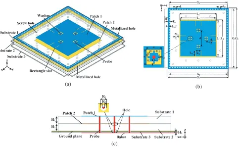
Figure 1 shows the geometry of the proposed antenna whose detailed dimensions are described in Table 1. Substrates 1 and 2 are F4B substrate layers with the same side length of G1. Two square patches are
etched on the same side of the F4B substrate with thickness of 5 mm and relative permittivity of 2.65. Patch 1 with a side length of 64 mm is etched on the top side of substrate 1. In order to improve the bandwidth, a pair of parallel rectangle slots is etched on each edge of patch 1 perpendicularly. As a result, an E-shaped patch is obtained. A further increase in the bandwidth is also possible through incorporating a small washer to cancel the reactance of the probe at the expense of increased complexity of the design and fabrication. Patch 2 with a side length of 67 mm is etched on the top side of substrate 2. Substrate 3 is an FR4 substrate layer, located at the bottom of the proposed antenna. Two microstrip baluns, printed on the backside of the FR4 substrate with thickness of 1 mm and relative permittivity of 4.4, are utilized to feed the antenna. Four vertical probes penetrating three substrates are used to transmit current. The dimensions of the four probes are identical, and each probe has vertical length 11 mm and width 1.3 mm. The washer is directly connected to the vertical probe. Patch 1 is electromagnetically coupled to the washer, while patch 2 is electromagnetically coupled to the vertical probe. Three substrates are placed together as shown in Fig. 1. Therefore, a stacked structure is introduced and enhances the bandwidth performance to some extent.
(a) (b)
(c)
Figure 1. Top and side views of the stacked-patch DBDP antenna. (a) 3-D view. (b) Top view. (c) Side view.
Table 1. Dimensions for the proposed dual-band dual-polarized antenna.
Parameters G1 G2 G3 L1 L2 Ls1 Ls2 Ws1
Values/mm 110 106 105 64 67 10 0.9 1
Parameters Ws2 d dr dp H1 H2 H3 R1
Values/mm 0.5 29 2 3 5 5 1 4
Parameters R2 Lbt Lrp Tp a b M3 Kw
Values/mm 1.3 6 2.5 4 5.8 3.2 5 9
the current flows through the metallized holes, the metallized holes periodically arranged form a closed electromagnetic wall, and the wall has gain-increasing characteristics similar to the classical rectangular cavity-shaped reflector.
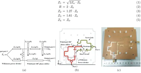
2.2. 180◦ Broadband Balun Design
The proposed balun structure comprises a Wilkinson power divider cascaded by a non-coupled-line broad-band 180◦ phase shifter as shown in Fig. 2(a). When the original signal is split into two ways, they pass through the two paths of the 180◦phase shifter to obtain a stable phase shifting, and the balun can operate across a reasonably broad band. As a design guideline, formulas (1)–(5) are presented for the balun design in a general way, whereZaand Zb stand for the input and output port impedances of the balun, respectively;Z1 stands for the characteristic impedance of the quarter wavelength
microstrip-lines in the power divider,Z2 stands for the characteristic impedance of the shunted open and the short
circuit λ/8 microstrip-lines used in the phase shifter;Z3 stands for the characteristic impedance of the
main microstrip-line;Z4stands for the characteristic impedance of the reference line. Here, it should be
mentioned that for Eqs. (3)–(4), we refer to [19] to get the optimized coefficients 1.27 and 1.61. Usually, the input impedance of the antenna and the output impedance of microstrip balun are 50 Ω to achieve a matching condition, and the proposed balun is designed to output signals with equal amplitude. Therefore, the input impedance Za and output impedance Zb of the microstrip balun are both set to 50 Ω.
Z1 =
2Za·Zb (1)
R = 2·Zb (2)
Z2 = 1.27·Zb (3)
Z3 = 1.61·Zb (4)
Z4 = Zb. (5)
(a) (b) (c)
Wilkinson power divider Wideband 180 phase shifter Za
Input port 1
Z1(λ g/4 )
Z1(λ g/4 ) R
Z2(λ g/8 )
Z2(λ g/8 ) Z3(λ g/2 )
Z2(λ g/8 ) Z2(λ g/8 )
Z4(λ g)
Output port 2
Output port 3 Zb Zb
B
Screw hole
Resistor
Port 1
Port 2
Short circuit d
A C
D
x
y
Wilkinson Power divider Wideband 180
phase shfiter
ο
ο
(a) (b)
2.5 3.0 3.5 4.0 4.5 5.0 5.5
150 160 170 180 190 200
Pha
se B
a
la
n
ce (d
eg
ree)
Frequency (GHz)
2.5 3.0 3.5 4.0 4.5 5.0 5.5
-40 -30 -20 -10 0
S
-parameters (d
B)
Frequency (GHz)
S11
S22
S32
S21
S31
Figure 3. SimulatedS-parameters and Phase differences of the two balanced ports.
The layout graph and fabricated photograph of the balun are shown in Fig. 2(b) and Fig. 2(c). Two 50-Ω SMA connectors were also used at the feed below the ground, and two 100-Ω surface mount chip resistors were employed at the balun. For the horizontal polarization (port 1), the first broadband balun is to supply probe A and probe B with wideband out-of-phase excitation. Similarly, for the vertical polarization (port 2), the second 180◦ broadband balun is to supply probe C and probe D with wideband out-of-phase excitation. The simulated S-parameters and phase differences of the designed balun are shown in Fig. 3, and it can be seen that the broadband balun delivers both equal amplitude power division and consistent 180◦ (±5◦) phase shifting over a wideband. As two baluns have the same design mechanism and dimensions, their simulation results also have great similarities. So we only show one of the simulation results for clarity.
3. ANALYSIS OF ANTENNA DESIGN
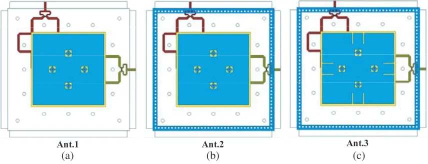
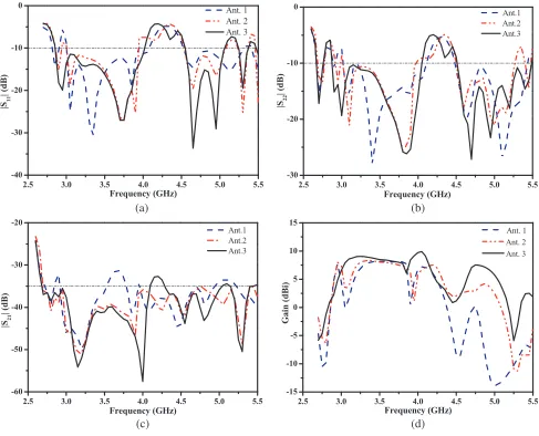
In order to explain the design process of the proposed antenna, three prototypes are illustrated in Fig. 4. Ant. 1 is a stacked DBDP patch antenna. Ant. 2 is designed by introducing an SIW structure. On the basis of Ant. 2, Ant. 3 is designed as the proposed antenna by etching eight rectangle slots on patch 1 to improve the impedance bandwidth. All the antennas are analyzed by ANSYS HFSS based on the
(a) (b) (c)
Ant.1 Ant.2 Ant.3
(a) (b)
(c) (d)
2.5 3.0 3.5 4.0 4.5 5.0 5.5
-40 -30 -20 -10 0
|S11
| (dB
)
Frequency (GHz)
Ant. 1 Ant. 2 Ant. 3
2.5 3.0 3.5 4.0 4.5 5.0 5.5
-30 -20 -10 0
Frequency (GHz)
|S22
| (
d
B
)
Ant.1 Ant.2 Ant.3
2.5 3.0 3.5 4.0 4.5 5.0 5.5
-60 -50 -40 -30 -20
|S21
| (d
B)
Frequency (GHz)
Ant.1 Ant.2 Ant.3
2.5 3.0 3.5 4.0 4.5 5.0 5.5
-15 -10 -5 0 5 10 15
Gain
(
d
Bi
)
Frequency (GHz)
Ant. 1 Ant. 2 Ant. 3
Figure 5. Comparison of three different antennas. (a)S11. (b) S22. (c)S21. (d) Gain.
finite-element method. It is worth to note that these antennas are composed of three substrates, and in order to ensure the rigor of the result comparison, all three antennas are excited by port 1. The corresponding simulated S-parameters and gain are shown in Fig. 5. In Fig. 5(a), it can be seen that Ant. 1 has two frequency bands with a low frequency band ranging from 3 GHz to 3.95 GHz and a high frequency band ranging from 4.52 GHz to 5.32 GHz. The gain of Ant. 1 is also shown in Fig. 5(d). However, the simulated results illustrate that the gain decreases dramatically in the upper band, and they are much lower at the frequency of 5 GHz. To solve the problem of low gain, we present Ant. 2 introducing the SIW structure. It can be observed from Fig. 5(d) that the gain of Ant. 2 is 3.2–8.3 dBi in lower band and 0–4.3 dBi in upper band when the SIW structure is introduced. Nevertheless, that of Ant. 1 is only 0–8.1 dBi in the lower band and−13.9–0.3 dBi in upper band. Comparison of the two designs illustrates that the proposal of the SIW structure can considerably improve the antenna gain. Meanwhile, the effect of SIW structure is not significant on the reflection coefficient of Ant. 1.
(a)
1.40e-2 A/m 2.00e+1 A/m
(c)
x y
(b)
(d)
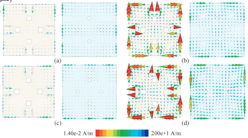
Figure 6. Surface currents on the two radiating patches. (a) Horizontal linear polarization at 3.7 GHz. (b) Horizontal linear polarization at 4.7 GHz. (c) Vertical linear polarization at 3.7 GHz. (d) Vertical linear polarization at 4.7 GHz.
Compared with Ant. 2 with a 10-dB impedance bandwidth of 27.1% (3–3.94 GHz) in port 1, the parallel rectangle slots have significant effect on the reflection coefficient. On the other hand, compared with Ant. 2, Ant. 3 impedance bandwidth of upper band is nearly unchanged, but the magnitude of S11
decreases at higher frequency band. Additionally, it can be observed from Fig. 5(d) that a high gain level of 0.5–9.3 dBi in lower band and 1.05–4.75 dBi in upper band can be achieved in Ant. 3, when the SIW structure and rectangle slot are introduced. The surface current of Ant. 3 on the two radiating patches is shown in Fig. 6. It can be concluded that port 1 excites same amplitude and out of phase currents along they-axis on two radiating patches, and port 2 excites same amplitude and out of phase currents along the x-axis because of the symmetric layout and broadband balun. The horizontal or vertical polarization of two patches is created independently by port 1 or 2.
4. FABRICATION AND MEASUREMENT RESULTS
The fabricated prototype of the proposed antenna is illustrated in Fig. 7, and its measured results of S-parameters (S11, S22, S21), antenna gain, antenna efficiency and far-field radiation pattern were
obtained by an Agilent N5230A network analyzer and a Satimo Starlab near-field measurement system.
4.1. S-Parameter
Figure 8 shows the measured and simulated reflection coefficients of the proposed antenna at port 1 and port 2. As shown in the reflection coefficient curves, the antenna exhibits wide impedance bandwidth at two ports. The measured impedance bandwidth (return loss>10 dB) of lower bandf1is 1310 MHz (2.7–
4.01 GHz) at port 1 and 1280 MHz (2.75–4.03 GHz) at port 2, respectively, which meet the bandwidth requirement (3.4–3.69 GHz) of antennas in WiMAX application. The impedance bandwidth (return loss >10 dB) of upper band f2 is also shown in Fig. 8. It can be seen that f2 is 940 MHz (4.36–5.3 GHz)
(a) (b)
Figure 7. (a) Radiating antenna and feeding network. (b) Assembled antenna.
2.5 3.0 3.5 4.0 4.5 5.0 5.5
-70 -60 -50 -40 -30 -20 -10 0
S
-param
e
te
r
s (dB
)
Frequency (GHz) Simu. S11 Simu. S21 Simu. S22 Meas. S11 Meas. S21 Meas. S22
Figure 8. Simulated and measuredS-parameters of the proposed antenna.
2.5 3.0 3.5 4.0 4.5 5.0 5.5
-10.0 -7.5 -5.0 -2.5 0.0 2.5 5.0 7.5 10.0 12.5
Gain (dBi
)
Frequency (GHz)
Simu. port1 Simu. port2 Meas. port1 Meas. port2
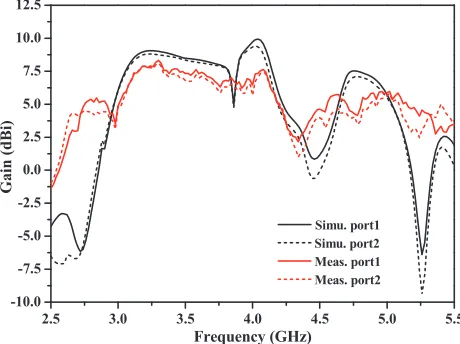
Figure 9. Simulated and measured gain of the proposed antenna for port 1 and port 2.
frequency across the entire impedance bandwidth (2.7–5.3 GHz) is more than 35 dB. Especially, the isolation can reach more than 38 dB when the proposed antenna works in the upper bandf2.
4.2. Gain
The gain characteristic of the proposed antenna is illustrated in Fig. 9. The antenna gain fluctuates within corresponding impedance bandwidth. At port 1, the measured gain of lower bandf1 fluctuates
from 3 dBi to 8.3 dBi. Meanwhile, gain of the upper band f2 is also shown in Fig. 9 with fluctuation
range from 2.6 dBi to 6 dBi. Simultaneously, the measured gain at port 2 is also shown in Fig. 9. It can be observed that gain of the lower bandf1 fluctuates from 3.1 dBi to 8.1 dBi, and the gain of upper
bandf2 fluctuates from 2 dBi to 5.8 dBi.
In comparison, the measured gain of the proposed antenna excited by port 1 is similar to the measured gain at port 2. On the other hand, measured average gains of f1 and f2 are 6.6 and 4.9 dBi
at port 1, respectively, with the corresponding peak gains of 8.3 and 6 dBi at 3.3 and 5.02 GHz. When the antenna is excited by port 2, measured average gains of f1 and f2 are 6.3 and 4.2 dBi, respectively,
Table 2. Simulated and measured gain of the proposed antenna.
Frequency (GHz) 2.7 3.3 3.9 4.4 4.8 5.2
Simulated Gain Port 1 (dBi) −5.8 9.0 8.4 1.9 7.4 −1.3 Simulated Gain Port 2 (dBi) −6.6 8.7 8.3 0.6 7.1 −2.6 Measured Gain Port 1 (dBi) 3.0 8.3 6.7 3.2 4.7 4.8 Measured Gain Port 2 (dBi) 4.1 8.1 6.3 2.1 3.7 3.2
and resistance are also not negligible. In the process of testing, the loss of the microstrip line and the internal resistance of the resistor consume too much energy, causing the measured gain less than the simulated gain.
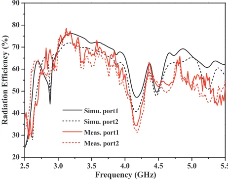
4.3. Radiation Efficiency
Figure 10 illustrates the simulated and measured efficiencies of the proposed antenna. It can be observed that the measured efficiency of the proposed antenna is between 50–78%, lower than the simulated one. The low efficiency may come from the feeding network, the high dielectric loss of FR4 substrate and the resistor of the broadband balun.
2.5 3.0 3.5 4.0 4.5 5.0 5.5
20 30 40 50 60 70 80 90
Radiation Efficiency (%)
Frequency (GHz) Simu. port1
Simu. port2 Meas. port1 Meas. port2
Figure 10. Simulated and measured efficiency of the proposed antenna for port 1 and port 2.
4.4. Radiation Patterns
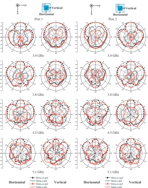
The horizontal and vertical plane radiation patterns of ports 1 and 2 within the operation bandwidth (2.75–4.01 GHz, 4.4–5.21 GHz) are measured and presented in Fig. 11. For comparison, simulated radiation patterns of port 1 and port 2 in the two planes are also shown in Fig. 11. While measuring radiation patterns at one port, another port is terminated by a 50 load. It can be observed from Fig. 11 that there is a good agreement between simulated and measured results, and the radiation patterns have good identity and higher than 20 dB cross-polarization suppression in the main beam, when port 1 is excited.
x y Horizontal Vertical x y Horizontal Vertical -40 -30 -20 -10 0 0 30 60 90 120 150 180 210 240 270 300 330 -40 -30 -20 -10 0 0 30 60 90 120 150 180 210 240 270 300 330 -40 -30 -20 -10 0 30 60 90 120 150 180 210 240 270 300 330 -40 -30 -20 -10 0 0 30 60 90 120 150 180 210 240 270 300 330 -40 -30 -20 -10 0 0 30 60 90 120 150 180 210 240 270 300 330 -40 -30 -20 -10 0 0 30 60 90 120 150 180 210 240 270 300 330 -40 -30 -20 -10 0 0 30 60 90 120 150 180 210 240 270 300 330 -40 -30 -20 -10 0 0 30 60 90 120 150 180 210 240 270 300 330 -40 -30 -20 -10 0 0 30 60 90 120 150 180 210 240 270 300 330 -40 -30 -20 -10 0 0 30 60 90 120 150 180 210 240 270 300 330 -40 -30 -20 -10 0 0 30 60 90 120 150 180 210 240 270 300 330 -40 -30 -20 -10 0 0 30 60 90 120 150 180 210 240 270 300 330 -40 -30 -20 -10 0 0 30 60 90 120 150 180 210 240 270 300 330 -40 -30 -20 -10 0 0 30 60 90 120 150 180 210 240 270 300 330 -40 -30 -20 -10 0 0 30 60 90 120 150 180 210 240 270 300 330 -40 -30 -20 -10 0 0 30 60 90 120 150 180 210 240 270 300 330
Horizontal Vertical Horizontal Vertical
Port 1 Port 2
0 3.0 GHz 3.0 GHz 3.8 GHz 3.8 GHz 4.5 GHz 4.5 GHz 5.1 GHz 5.1 GHz
efficiently in both horizontal and vertical polarizations. However, the measured cross polarization has a difference from the simulated one. This discrepancy of the radiating patterns should be caused by two reasons. One is the inevitably introduced air layer when three substrates are combined by plastic screws, and the other reason is the experiment tolerance.
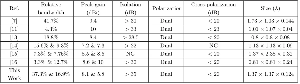
4.5. Comparison
The measured characteristics of the proposed antenna are compared with previous works in Table 3. We can find that the proposed antenna in this paper has the characteristics of dual frequencies, dual polarizations, wide impedance bandwidth, high isolation, and low cross polarization.
Table 3. Performance comparisons with typical reported antennas.
Ref. Relative bandwidth
Peak gain (dBi)
Isolation
(dB) Polarization
Cross-polarization
(dB) Size (λ)
[7] 41.7% 9.4 >30 Dual <20 1.73×1.03×0.144
[11] 4.3% 10 >33 Dual <23 1.01×1.07×0.04
[13] 18.8% 8.4 >28.5 Dual <20 0.8×0.8×0.08
[14] 15.6% & 9.3% 7.2 & 7.3 >22 Dual NG 1.13×1.13×0.09 [15] 7.3% & 7.76% 8.5 & 8.5 NG Dual <20 1.37×2.38×0.32 [16] 3.3% & 12.7% 8.6 & 10 >30 Dual <20 0.81×0.81×0.24
This
Work 37.3% & 16.9% 8.1 & 5.8 >35 Dual <20 1.37×1.37×0.124
λ0 is the wavelength at the center frequency of the lower working band. NG: not given.
5. CONCLUSION
A broadband dual-band dual-polarized patch antenna covering the WiMAX and WLAN bands is developed. The proposed antenna consists of three-layer substrates fed by a broadband balun feeding network for 37.3% and 16.9% relative bandwidths. The stacked layout, broadband balun, rectangle slot and capacitive washer are adopted to enhance the bandwidth. A balanced feeding with 180 phase shifts is also used to realize the high isolation about 35 dB, high cross-polarization suppression up to 20 dB at broadside and the characteristic of dual polarizations. The proposed antenna can be used in wireless communication such as WiMAX and WLAN.
ACKNOWLEDGMENT
This work is supported by the National Natural Science Foundation of China under Grant 61172020.
REFERENCES
1. Roy, A., S. Bhunia, D. C. Sarkar, and P. P. Sarkar, “Slot loaded compact microstrip patch antenna for dual band operation,”Progress In Electromagnetics Research C, Vol. 73, 145–156, 2017. 2. Quevedo-Teruel, ´O., M. N. Moukehn, and E. Rajo-Iglesias, “Dual-band patch antennas based on
short-circuited split ring resonators,” IEEE Trans. Antennas Propag., Vol. 59, No. 8, 2758–2765, Aug. 2011.
4. Han, L. P., W. M. Zhang, X. W. Chen, G. R. Han, and R. B. Ma, “Design of compact differential dual-frequency antenna with stacked patches,” IEEE Trans. Antennas Propag., Vol. 58, No. 4, 1387–1392, Apr. 2010.
5. Liu, S., W. Wu, and D. G. Fang, “Single-feed dual-layer dual-band E-shaped and U-slot patch antenna for wireless communication application,” IEEE Antennas Wireless Propag. Lett., Vol. 15, 468–471, 2016.
6. Matin, M. A., B. S. Sharif, and C. C. Tsimenidis, “Probe fed stacked patch antenna for wideband applications,” IEEE Trans. Antennas Propag., Vol. 55, No. 8, 2385–2388, Aug. 2007.
7. Xian, J. Z., X. Q. Lin, L. Y. Nie, J. W. Yu, and Y. Fan, “Wideband dual-polarization patch antenna array with parallel strip line balun feeding,”IEEE Antennas Wireless Propag. Lett., Vol. 15, 1499– 1501, 2016.
8. Mak, K. M., X. Gao, and H. W. Lai, “Low cost dual polarized base station element for long term evolution,”IEEE Trans. Antennas Propag., Vol. 62, No. 11, 5861–5865, Nov. 2014.
9. Jin, Y. Y. and Z. W. Du, “Broadband dual-polarized F-probe fed stacked patch antenna for base stations,” IEEE Antennas Wireless Propag. Lett., Vol. 14, 1121–1124, 2015.
10. Wu, C. S., C. L. Lu, and W. Q. Cao, “Wideband dual-polarization slot antenna with high isolation by using microstrip line balun feed,” IEEE Antennas Wireless Propag. Lett., Vol. 16, 1759–1762, 2017.
11. Gao, Y., R. B. Ma, Y. P. Wang, Q. Y. Zhang, and C. Parini, “Stacked patch antenna with dual-polarization and low mutual coupling for massive MIMO,”IEEE Trans. Antennas Propag., Vol. 64, No. 10, 4544–4549, Oct. 2016.
12. Jin, H. Y., K. S. Chin, W. Q. Che, C. C. Chang, H. J. Li, and Q. Xuan, “Differential-fed patch antenna arrays with low cross polarization and wide bandwidths,”IEEE Antennas Wireless Propag. Lett., Vol. 13, 1069–1072, 2014.
13. Deng, C. J., Y. Li, Z. J. Zhang, and Z. H. Feng, “A wideband high-isolated dual-polarized patch antenna using two different balun feedings,”IEEE Antennas Wireless Propag. Lett., Vol. 13, 1617– 1619, 2014.
14. Zhai, H. Q., K. D. Zhang, and D. Feng, “A low-profile dual-band dual-polarized antenna with an AMC surface for WLAN applications,”IEEE Antennas Wireless Propag. Lett., Vol. 16, 2692–2695, 2017.
15. Sabri, L., N. Amiri, and K. Forooraghi, “Dual-band and dual-polarized SIW-Fed microstrip patch antenna,” IEEE Antennas Wireless Propag. Lett., Vol. 13, 1605–1608, 2014.
16. Row, J. S., and Y. J. Huang, “Dual-band dual-polarized antenna for WLAN applications,”Microve and Optical Technology Letters, Vol. 60, No. 1, 260–265, Jan. 2018.
17. Ge, L. and K. M. Luk, “A low-profile magneto-electric dipole antenna,” IEEE Trans. Antennas Propag., Vol. 60, No. 4, 1684–1689, Apr. 2016.
18. Oliver, C., L. Sam, A. Sam, V. G. Dries, and D. Piet, “Half-mode Substrates-Integrated-Waveguide cavity-backed slot antenna on cork substrate,”IEEE Antennas Wireless Propag. Lett., Vol. 15, 162– 165, 2016.