Multi-Level Inverter Capable Of Power
Factor Control with DC Link Switches
A.G. Karthikeyan, P. Sathyanathan, S. Saravanan, M. Vimala
Department ofElectrical and Electronics Engineering, Magna College of Engineering, Chennai, India
ABSTRACT: this paper proposes a new multi-level inverter topology based on a H-bridge structure with four switches connected to the dc-link. Based on a POD (Phase opposition disposition) modulation method, a new PWM method which requires only one carrier signal is suggested. The switching sequence to balance the capacitor voltage is also considered. In addition to these, the proposed topology requires minimum number of component count to increase the number of voltage level. Operating principle of the proposed inverter is verified through simulation and experiment.
I. INTRODUCTION
Due to the increasing demand on the renewable energy sources, grid connected inverter systems are becoming more and more important than ever before. For grid connected operation, the inverter should meet the following requirements.
1. The inverter has to generate a pure sinusoidal output voltage.
2. The inverter output current should have low total harmonic distortion (THD).
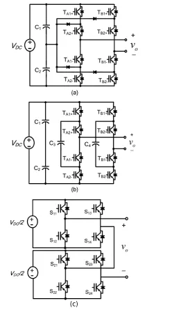
Traditionally, two-level PWM inverter is used for grid-tied operation. In case of a two-level inverter, the switching frequency should be high or the inductance of the output filter inductor need to be big enough to satisfy the required THD. To cope with the problems associated with the two-level inverter, multi-level inverters (MLIs) are introduced for gridconnected inverter. Several MLI topologies have been suggested so far and they can be mainly classified as three types in Fig. 1; neutral point clamped (NPC), flying capacitor (FC), and cascaded type [3-5].
Advantage of the MLIs is that their switching frequency and device voltage rating can be much lower than those of a traditional two-level inverter for the same output voltage. Therefore, IGBT switching loss can be reduced significantly and thus the inverter system efficiency can be increased [6-8].
(c)
Fig. 1. Topologies of multi-level inverters. (a) neutral point clamped (NPC) type. (b) Flying capacitor (FC) type. (c) Cascade type.
II. PROPOSED MULTI-LEVEL INVERTER
A.Topology of multi-level inverter
As shown in Fig. 2, the proposed MLI is composed of two dc-link capacitors (C1, C2) and four switching devices (TA+,
TA-, TB+, TB-) comprising a H-bridge, and four active switches (TP+, TP-, TN+, TN-) located between dc-link and
frequency. Whereas, voltage across the switching devices in the H-bridge (TA+, TA-, TB+, TB-) is VDC and the switches
(TA+, TA-, TB+, TB-) are switched at a frequency of the fundamental component of the output voltage (e.g. 50 or 60 Hz).
Thus, the dc-link switches (TP+, TP-, TN+, TN-) and the Hbridge switches (TA+, TA-, TB+, TB-) can be strategically selected
based on the rated power of the inverter system in order to reduce system cost and increase efficiency. Table I shows the output voltage according to the switching states.
Fig. 2. Proposed single-phase multi-level inverter topology.
TABLE I
Output voltage according to switching states Output
voltage (Vo)
Switching condition TP+ TP- TN+ TN- TA+,
TB-
TA-, TB+ VDC ON OFF OFF ON ON OFF
VDC /2
OFF ON OFF ON ON OFF ON OFF ON OFF ON OFF
0 OFF ON ON OFF ON OFF OFF ON ON OFF OFF ON
-VDC /2
OFF ON OFF ON OFF ON ON OFF ON OFF OFF ON -VDC ON OFF OFF ON OFF ON
TABLEII
Operating mode of the proposed MLI Operating mode Reference voltage range Output voltage Mode 1 Vc≤vref<2Vc VDC/2 or
VDC Mode 2 0≤vref<Vc 0 or VDC
Mode 3 -Vc≤vref<0 -VDC/2 or 0
Mode 4 -2Vc≤vref<-Vc -VDC or
B.Operating modes and proposed PWM strategy
The output voltage of the proposed MLI shown in Fig. 2 has five levels (VDC, VDC/2, 0, -VDC/2, -VDC) according to the
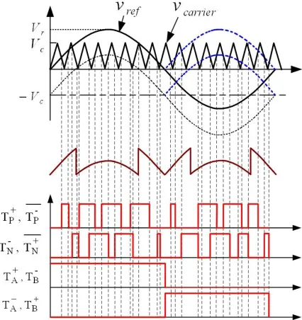
switching states of the inverter. There are four operation modes depending on the instantaneous value of the reference voltage, vrefand the maximum value of the carrier signal, VC(see Fig. 4). Table II shows the possible inverter output
voltage level according to the operating mode.
In case of the N-level NPC type multi-level inverter, N-1 triangular carrier signals with the same frequency and amplitude are used so that they fully occupy contiguous bands over the range +VDC to -VDC. A single sinusoidal
reference is compared with each carrier signalto determine the output voltage for the inverter. Three dispositions of the carrier signal are considered to generate the PWM signal [9-11].
1) Phase disposition (PD); where all carriers are in phase.
2) Alternative phase opposition disposition (APOD); where each carrier is phase shifted by 180 degree from its adjacent carrier.
3) Phase opposition disposition (POD); where the carriers above zero voltage are 180 degree out of phase with those below zero voltage.
Fig. 3 shows the reference signal and the carrier signal arrangements for PD modulation, POD modulation, and APOD modulation.
A new PWM strategy based on POD modulation which requires only a single carrier signal (vcarrier) is proposed and the detailed PWM strategy is depicted in Fig. 4. If the
Fig. 3. Carrier and reference signal arrangements for: (a) Phase disposition (PD). (b) Alternative phase opposition disposition (APOD). (c) Phase opposition disposition (POD).
reference signal is positive, then the switch pair (TA+, TB-) are turned on, and if it is negative, then the switch pair (TA-,
TB+) are turned on. Thus the switches composing the H bridge inverter turned on and turned off once during the period
complementally to the switches (TP+, TN-). The generation of the PWM signal for dc-link switches (TP+, TN-) can be
explained as follows.
∙Mode 1: a signal subtracted from the reference signal by
Vc is compared with the carrier signal. If vref-Vc>vcarrier, then all switches TP+ and TN- are turned on. If vref-Vc<vcarrier,
then the switch TP+ or TN- is turned off alternately.
∙ Mode 2: the reference signal is directly compared with a carrier signal. If vref>vcarrier, then the switch TP+ or TN- is
turned on alternately. If vref<vcarrier, then all switches TP+ and TN- are turned off.
∙ Mode 3: -vref is directly compared with a carrier signal.
If -vref>vcarrier, then the switch TP+ or TN- is turned on alternately. If -vref<vcarrier, then all switches TP+ and TN- are turned
off.
∙ Mode 4: a signal subtracted from -vref by Vc is compared with the carrier signal. If If -vref-Vc>vcarrier, then all switches
TP+and TN- are turned on. If-vref-Vc<vcarrier, then the switch TP+ or TN- is turned off alternately.
Only one carrier signal is used to generate eight PWM signals in the proposed PWM method. Thus it is quite simple.
Fig. 4. PWM strategy based on POD with single carrier signal
C.Voltage balancing of dc-link capacitor
One of the important issues about multi-level inverter is the voltage balance of the dc-link capacitor. The voltage of capacitor C1 and C2 should be equally balanced to VDC/2. However the midpoint voltage fluctuates when C1 and C2
To solve this problem, the switching state should be selected appropriately in Fig. 5. If only one switch in a dc- link is turned on, the output voltage becomes VDC/2. In order to balance the voltage of dc-link capacitor, dc-link switches (TP+,
TN-) are alternately turned on at mode 2, and alternately turned off at mode 1. And switches (TP-, TN+) are operated
complementally to switches (TP+, TN-). Therefore, the switching sequence of mode 1 is (a)-(b)-(a)-(c), and the switching
sequence of mode 2 is (d)-(b)-(d)-(c). The switching sequence of mode 3 and mode 4 are similar that of mode 1 and mode 2. The switching sequence of mode 3 is (h)-(f)-(h)(g), and the switching sequence of mode 4 is (e)-(f)-(e)-(g).
(g) (h)
Fig. 5. Switching states of the proposed inverter in one cycle.(a) state 1 : vo=
0. (b) state 2 : vo= VDC/2. (c) state 3 : vo= VDC/2. (d) state 4 : vo= VDC. (e) state 5 : vo= 0. (f) state 6 : vo= -VDC/2. (g) state
7 : vo= VDC/2. (h) state 8 : vo=
Fig. 6. Proposed 9-level inverter topology
D.Extension to 9-level inverter
It should be noted that although the number of the switching devices in the proposed 5-level inverter (shown in Fig. 2) is the same as that of the conventional cascaded H-bridge MLI, the switches (TA+, TA-, TB+, TB-) in the proposed MLI
are switched at a low frequency(60 Hz). Moreover, unlike the cascaded H-bridge MLI, the proposed 5-level inverter requires only one isolated voltage source, VDC.
In order to maximize the effectiveness of the proposed MLI, 9-level inverter which was extended from 5-level inverter shown in Fig. 2 is also proposed in this paper and the overall circuit diagram is shown in Fig. 6. As shown in Fig. 6, in case of 9-level inverter, the proposed inverter requires less active devices than 9-level cascaded H-bridge MLI. Therefore, number of switching devices in the proposed MLI can be reduced significantly as the number of voltage level increases.
III.SIMULATION AND EXPERIMENTAL RESULTS
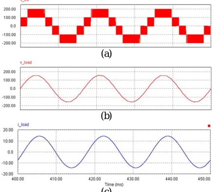
The proposed 5-level inverter is tested to verify the operating principle of the proposed MLI. The LC filter is inserted between the output of the inverter and the load. Electrical specifications of the proposed inverter are summarized in Table III. Fig. 7 and 8 show simulation waveforms of the proposed inverter in 5-level. Fig. 7 shows the waveforms of the inverter output voltage, load voltage and the load current when the power factor becomes unity. Fig. 8 shows the waveforms of the inverter output voltage, load voltage and the load current during the lagging power factor.
TABLEIII
Electrical specifications of the proposed single-phase 5-level inverter dc-link voltage 200V
Output voltage 110 Vrms
dc-link capacitor 2200 uF Filter inductor (Lf) 300 uH
Filter capacitor (Cf) 150 uF
Switching frequency (fsw)
5 kHz
Output frequency (fo)
(a)
(b)
(c)
Fig. 7. Waveforms of 5-level inverter (Load : R = 9.3 Ω). (a) Output voltage of the inverter. (b) load voltage. (c) load current.
(a)
(b)
(c)
Fig. 8. Waveforms of 5-level inverter (Load : R = 9.3 Ω, L = 14.9mH). (a) Output voltage of the inverter. (b) load voltage. (c) load current.
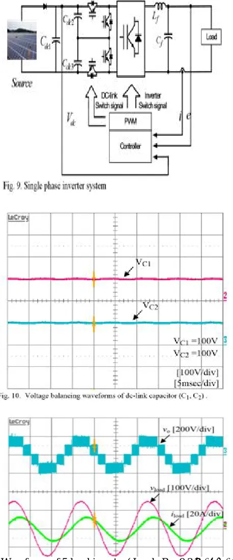
Based on the simulation results, the experiment was conducted. Rating and the parameters of the system which was used in the experiment are the same with those of the simulation. Configuration for the experiment is shown in Fig. 9. Fig. 10 shows that the capacitor voltages (VC1, VC2) are controlled constantly. The capacitor voltages (VC1, VC2) are
IV. CONCLUSION
This paper proposed a new multi-level inverter topology based on a H-bridge inverter with four switches connected to the dc-link. The proposed MLI has the following advantages over the conventional inverters.
1. Number of devices of the proposed multi-level inverter is fewer than that of the conventional multi-level inverters. Therefore, the proposed system is more reliable and cost competitive than the conventional two-level and multilevel inverters.
2. The four switches (TA+, TA-, TB+, TB-) in the H-bridge are switched at a low frequency (e.g. 60 Hz). Therefore,
switching loss of The four switches (TA+, TA-, TB+, TB-) is almost negligible.
3. Only one carrier signal is required to generate the PWM signals for 4 switching devices (TP+, TP-, TN+, TN-).
4. The proposed topology can be easily extended to 9-level or higher level with minimized active device component count.
ACKNOWLEDGMENT
This work was supported by the Power Generation & Electricity Delivery of the Korea Institute of Energy Technology Evaluation and Planning (KETEP) grant funded by the Korea government Ministry of Knowledge Economy
(No. 20111020400260)
REFERENCES
1. G. Grandi, C. Rossi, D. Ostojic, D. Casadei, "A New Multilevel Conversion Structure for Grid-Connected PV Applications", IEEE Trans. Ind. Electron., vol. 56, no. 11, pp. 4416-4426, Nov. 2009.
2. N. A. Rahim, S. Mekhilef, “Implementation of Three- Phase grid Connected Inverter for Photovoltaic Solar Power Generation System” Proceedings IEEE. PowerCon 2002. Vol. 1, pp. 570-573., Oct 2002
3. A. Nabae, I. Takahashi and H. Akagi, “A New Neutral-Point-Clamped PWM Inverter” IEEE Trans. Ind. Appl., vol. 1A-17, no. 5, pp. 518-523, Sep. 1981.
4. Y. Liang, C.O. Nwankpa, "A power-line conditioner based on flyingcapacitor multilevel voltage source converter with phase-shift SPWM" IEEE Trans. Industrial Electronics, Vol. 36, pp. 965-971, 2000.
5. E. Villanueva, P. Correa, M. Pacas, “Control of a Single-Phase Cascaded H-Bridge Multilevel Inverter for Grid-Connected Photovoltaic Systems”, IEEE Trans. Industrial Electronics, Vol. 56, pp. 4399-4406, 2009.
6. O. Lopez, R. Teodorescu, J. Doval-Gandoy, "Multilevel transformerless topologies for single-phase grid-connected converters" IEEE. IECON 2006, pp. 5191-5196, 2006.
7. Tae-Jin Kim, Dae-Wook Kang, Yo-Han Lee and Dong-Seok Hyun, “The analysis of conduction and switching losses in multi-level inverter system”, PESC. 2001 IEEE Vol. 3, pp 1363-1368, 2001.
8. D.A.B. Zambra, C. Rech, J.R. Pinheiro, "Comparison of Neutral-PointClamped, Symmetrical, and Hybrid Asymmetrical Multilevel Inverters", IEEE Trans. Ind. Electron., Vol. 57, no. 7, pp2297-2306, July 2010.
9. M. Calais, "Analysis of multicarrier PWM methods for a single-phase five level inverter", PESC. 2001 IEEE, Vol. 3, pp. 1351-1356, 2001. 10. B.P. McGrath, “Multicarrier PWM strategies for multilevel inverters”, IEEE Trans. Ind. Electron., Vol. 49, no. 4, pp. 858-867, 2002.