Design & Analysis of Adiabatic Logic based
Multiplexers for Ultra Low Power
Applications
Samik Samanta1, Rajat Mahapatra2, Ashis Kumar Mal3
Assoc. Prof, Department of ECE, Neotia Institute of Technology, Management & Science Kolkata,
West Bengal, India1
Assoc. Prof, Department of ECE, National Institute of Technology, Durgapur, West Bengal, India 2,3
ABSTRACT: Minimization of power consumption in portable and battery powered embedded systems has become an important aspect of processor and system level designs. Opportunities for power optimization and tradeoffs emphasizing low power are available across the entire design hierarchy.Autonomy of power supply used in portable devices directly depends on efficiency of digital logic circuits. Digital systems beside high processing power must have very low power consumption. The power consumption of the electronic devices can be reduced by adopting different design styles. Adiabatic logic style is said to be an attractive solution for such low power electronic applications. By using Adiabatic techniques energy dissipation in PMOS network can be minimized and some of energy stored at load capacitance can be recycled instead of dissipated as heat. Here in this paper positive feedback adiabatic logic based multiplexer is presented. Power dissipation of PFAL multiplexer is compared with CMOS and ECRL multiplexers.
KEYWORDS:VLSI, Adiabatic, ECRL, PFAL, Quasi adiabatic.
I. INTRODUCTION
With the recent trend toward portable computing and communication, power dissipation has become one of the major design concerns along with chip area and device performance. Research to reduce power dissipation at various levels of design abstraction has started to achieve ultra-low power dissipation with optimum performance. As the transistor count per chip increases rapidly significant reduction in power overhead and leakage is of particular importance [2]. In today’s world the circuit complexity and processing speed are rapidly increasing whereas silicon area has to be as minimal as possible. This has resulted in the exponential rise in heat generated per unit silicon area. The range and applications of digital systems are increasing day by day in portable and embedded computing. Issues such as battery operation time, weight, size demand dramatic reduction in power or energy dissipation. It is anticipated that the expected battery life time will not increase by more than 30% over the next few years [7]. In the absence of low power design techniques, future portable systems will suffer a lot from very short battery life time and oversize battery packs. The design engineers of high-end systems also face challenge of the increasing power dissipation with the increase in area-frequency and power delay product. The packaging and cooling strategies will have to be refined putting an extra overhead on the cost. In addition to cost and system design issues, the reliability is also affected by the high temperature. Very high temperature causes electro migration, gate dielectric breakdown and other silicon failure mechanisms. All these have fuelled the research activity in low power design for VLSI circuits. Now days the portable electronics has made low power circuit design extremely desirable. All efforts eventually converge on decreasing the power consumption entailed by ever shrinking size of the circuits enabling the portable gadgets. Reducing power supply voltage is a straightforward method to achieve low power consumption. The low power and low voltage CMOS techniques were applied extensively in analog, digital and mixed mode circuits for the compatibility with the present IC technologies. Low power dissipation is attractive, and perhaps even essential in these applications to have reasonable battery life and weight. The ultimate goal in design is close to having battery- less systems.
II. ADIABATIC LOGIC
The term “adiabatic” describes a thermodynamic process in which there is no energy exchange with the environment, and therefore no dissipation of energy or power occurs [5]. But in VLSI, as the transfer of the electric charge takes place between the nodes of a circuit, various techniques can be applied to minimize this energy loss during this charge transfer process. Adiabatic technology is basically used to reduce the energy dissipation during the switching process and further reuse some of the energy by recycling it from the load capacitance[1]-[3]. For recycling, the adiabatic circuits use the constant current source power supply and for reduce dissipation it uses the trapezoidal or sinusoidal power supply voltage Energy recovery principle can be best understood by comparing the energy dissipation in conventional CMOS circuit with that of adiabatic switching circuit. CMOS technology has been selected for low power digital design because of its negligible static power dissipation. The leakage currents and sub-threshold injection currents give rise to a static component of CMOS power dissipation. The short circuit power dissipation is also low because it occurs for a very short time. The major contributor is dynamic power dissipation which results from charging and discharging of the load capacitor. In case of CMOS inverter, when the input is logic zero, PMOS connects Vdd to
the load capacitor CL and a charge equals to Q = CL Vdd is stored on the load capacitance. The energy consumed to store
this charge is Q. Vdd =CL (Vdd)2. Fifty percent of this energy is dissipated in the PMOS and it is independent of
resistance of the PMOS and charging time. The remaining fifty percent energy is stored on the CL. When the inputs are
inverted then the energy stored on the CL is dissipated in the nFET. The energy dissipated in charging and discharging
the load capacitor in one input cycle is CLVdd2 and it is dissipated as a heat. The amount of energy lost is exactly twice
the signal energy. To minimize the energy dissipation if we reduce the signal energy then it will also increase sensitivity to background noise. It is therefore important to reduce the switching energy of MOS based circuits [6]. In case of MOSFET, the controlling charge is on the gate and the controlled charge flows from drain to source in the channel. The energy is dissipated in the PMOS or NMOS because of the resistance offered by the channel of the MOSFET to this controlled charge. The energy that would be dissipated in the channel can be minimized if this charge transport in the channel is slowed down. A constant current source can be used to deliver a charge of CL Vdd for a time
T. The energy dissipation in the transistor will be,
E= P x T=I2RT= (CLVdd2/T)x Rx T………… (1)
E= (RxCL/T)x CLVdd2 ……… (2)
Equations1 and 2 indicates that it is possible to reduce the energy dissipation by using a constant current source instead of constant voltage source and increasing charging or discharging time T. This principle is called ‘adiabatic charging’. The term adiabatic is taken from Thermodynamics and it means without the flow of heat[7]. In adiabatic switching circuit, the energy dissipation can be reduced to an arbitrary degree. Instead of using a separate power supply for Vdd
and for clock, the clock signal can be reshaped and be used for both the purposes. This clock signal is called power-clock. The power-clock voltage is in the form of a ramp or sinusoidal signal. The power-clock supply charges the load capacitor adiabatically during the time it is ramping up. The load capacitor energy recycles back when it is ramping down. This adiabatic cycling of energy between the logic circuit load and the power-clock supply needs an adiabatic path. It is possible to have the same path for charging and discharging reversibility but it is recommended to have separate paths for charging and discharging.
The energy dissipation in standard circuits occurs when electrical currents are driven through transistors with a finite on-resistance and resistive signal lines. The resistive losses are proportional to the voltage difference for example between the terminals of a transistor device, which gives rise to the approach of limiting this voltage difference and avoiding abrupt currents. Let us consider a static CMOS inverter gate in represents information by the output node voltage, and dissipates all of the signal energy during the operation. During a switching event, either the up or pull-down network loses energy.
Examples of fully adiabatic logic are pass transistor adiabatic logic (PAL), split rail charge recovery logic (SCRL) etc. The examples of quasi or semi adiabatic logic are NMOS energy recovery logic (NERL), positive feedback adiabatic logic (PFAL) etc.
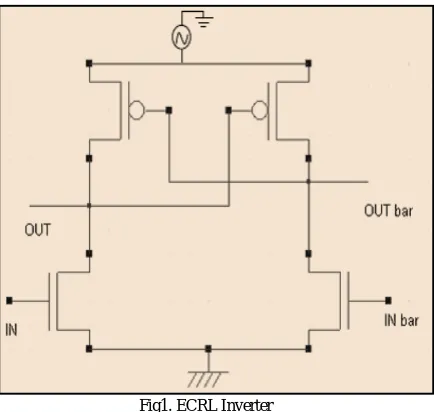
Full adiabatic structures cannot be achieved because a digital system cannot be isolated from the external environment completely. Hence it can be asymptotically achieved. But the complexity of the adiabatic circuit is high because they have forward and backward logic paths due to reversible logic. The full adiabatic circuits use logic switches and isolation switches. Quasi-adiabatic circuits do not require isolation switches and hence consume less silicon area [7]. ECRL performs precharge and evaluation simultaneously. It dissipates less energy as it does not use any precharge diode.ECRL has the same circuit structure as cascade voltage switch logic with differential switching. The circuit schematic of a simple ECRL inverter is shown in fig1.
Fig1. ECRL Inverter
The signals are dual rail type. The input applied is a pulse type signal. If the inverters are to be cascaded then multi-phase clock supply needs to be applied. This will allow the next stage to evaluate logic values in the precharge and evaluation phase when the present stage is in the hold state.
The primary advantage of PFAL over ECRL is that the functional blocks are in parallel with the PMOSFETs. This type of connection forms a transmission gate structure. The structure has the advantage of implementing both the true and complementary logic.
III.ADIABATIC MULTIPLEXER
Multiplexer is a digital switch. It allows digital information from several sources to be routed onto a single output line. The basic multiplexer has several data input lines and a single output line. The selection of a particular input line is controlled by a set of selection lines. Normally, there are 2ninput lines and n selection lines whose bit combinations
determine which input is selected. Therefore, multiplexer is many into one and it provides the digital equivalent of an analog selector switch. The 4x1 multiplexer has four inputs and one output. In addition, it has two selection lines. Depending on the two selection lines, one output is selected at a time from among the four input lines.
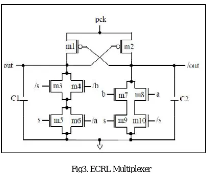
The schematic diagrams of ECRL multiplexer and PFAL multiplexer are presented below. The circuits are designed using minimum number of transistors. Both the circuits are driven by power clock. They are designed using energy recovery logic.
Fig3. ECRL Multiplexer
The simulation results of both the multiplexers are shown. They are simulated using PSPICE simulation software.
Fig 5. Simulation of ECRL Multiplexer Fig 6. Simulation of PFAL Multiplexer
TABLE I. POWER DISSIPATION OF VARIOUS MULTIPLEXERS
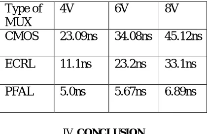
TABLE II. DELAY COMPARISON OF VARIOUS MULTIPLEXERS
IV.CONCLUSION
Positive feedback adiabatic logic inverter based inverter and multiplexer has minimum power dissipation than CMOS and ECRL based multiplexers. The power saving amount of PFAL based circuit over ECRL is approximately 60% in case of inverter and it is nearly 70% for multiplexers. PFAL based multiplexers can be used in various low power applications. They can be used in low power wireless and embedded SOC designs for their low power dissipations. PFAL multiplexers are suitable for ultra low power applications like high speed low power processors, reconfigurable systems and low power wireless applications.
Type of MUX
4V 6V 8V
CMOS 150fJ 350fJ 600fJ
ECRL 66fJ 80fJ 190fJ
PFAL 31fJ 47fJ 69fJ
Type of
MUX
4V
6V
8V
REFERENCES
[1] N. Weste and K. Eshraghian, Principles of CMOS VLSI Design A Systems Perspective, 2nd ed. New York:Addison Wesley,1993.
[2] M. Pedram, “Power minimization in IC design: principles and applications,” ACM Transactions on Design Automaton of Electronic Systems, 1(1): 3-56,January 1996.
[3] W. C. Athas, L. J. Svensson, J. G. Koller, et al., “Low powerdigital systems based on adiabatic-switching principles,” IEEE Trans. on VLSI Systems, 2(4): 398- 407, December 1994.
[4] J. S. Denker, “A review of adiabatic computing,” inProc. of the Symposium on Low Power Electronics,1994, pp. 94-97 [5] Jan Rabey, Massoud Pendram, Low power Design Methodologies:5-7,Kluwer Academic Publishers,5th edition.2002
[6] PD Khandekar, S Subbaraman ,Manish Patil “Low power Digital Design Using Energy-Recovery Adiabatic Logic” International
Journal of Engineering Research and IndustrialApllications,Vol1,No.III,pp199-2081994, pp. 94-97.
[7] S.Samanta “Adiabatic Computing” a contemporary review” 4th International conference on computer and devices for communication: codec 09. Kolkata 2009.
[8] S.Samanta“ Power Efficient VLSI Inverter Design using Adiabatic Logic and Estimation of Power dissipation using VLSI- EDA Tool” Special issue of International Journal of computer communication Technology.vol 2.isuue 2,3,4.pp300-303. 2010.
[9] L.Svensson “Adiabatic Switching” in low power Digital CMOS Design, Kluwer Academic Publisher, 1995. [10] J.Rabacy, Digital Integrated Circuits,PHI,1996.
[11] Dickinson, A.G. and Denker, J.S., Adiabatic Dynamic Logic,IEEE J. Solid-State Circuits, 1995, vol.30, no. 3,pp.311–315. [12] V.I Starosel, Adiabatic Logic Circuits: A Review, Russian Microelectronics, 2002, Vol.31, No. 1, pp.37-58.
[13] Y. Takahashi, Y. Fukuta, T. Sekine, and M. Yokoyama,2PADCL : Two Phase drive Adiabatic Dynamic CMOS Logic,Proc. IEEE APCCAS, Dec 2006, pp. 1486-1489.
[14] Denker, J.S., A Review of Adiabatic Computing, Proc.1994 Symp. on Low Power Electronics, San Diego,1994.
[15] S. Kim, C. Ziesler, and M. C. Papaefthymiou, “A true single- phase 8-bit adiabatic multiplier,” in Proc. 38th ACM/IEE Design Automation Conference, June 2001.
[16] J. Kim, C. H. Ziesler, and M. C. Papaefthymiou, “Energy recovering static memory,” in Proceedings of International Symposium on Low- Power Electronics and Design, Aug. 2002.
[17] C. H. Ziesler, J. Kim, and M. C. Papaefthymiou, “Energy recovering ASIC design,” in Proceedings of International Symposium on VLSI, Feb.[18] Y. Ye, K. Roy, Reversible and quasi-static adiabatic logic, inEuropean Conf. Circuit Theory and Design, 1997, pp. 912–917.
[19] D. Hongyy, Z. Runde, G. Yuanqing, High efficient charg recovery logic for adiabatic computing, ASIC2001,September, 2001.